
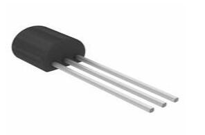
onsemi BSS84LT1G surprises in simple home electronics


P-Channel Cut Tape (CT) 10 Ω @ 100mA, 5V ±20V 30pF @ 5V TO-236-3, SC-59, SOT-23-3
onsemi BSS84LT1G delivers reliable, cool, and efficient switching for home electronics, excelling in low-power LED, relay, and sensor control applications.
Product Introduction
The onsemi BSS84LT1G stands out in simple home electronics projects. Hobbyists often expect basic performance from such a compact P-channel MOSFET, but this device surprises with its consistent switching and minimal heat generation. Users report smooth operation in LED control and relay circuits. Many find it reliable even under frequent use. These results make it a strong choice for those who want dependable results in low-power applications.
Key Specs
Switching
The onsemi BSS84LT1G offers specifications that fit many low-power home electronics projects. Its maximum drain-source voltage reaches -50 volts, which allows safe operation in circuits with moderate voltage requirements. The device supports a continuous drain current of 130 milliamps. This current rating works well for controlling small loads, such as indicator LEDs or miniature relays.
The table below summarizes the key electrical characteristics:
| Parameter | Value |
|---|---|
| Maximum Drain-Source Voltage (V(BR)DSS) | -50 V |
| Continuous Drain Current (ID) | 130 mA |
| Maximum RDS(on) @ VGS = 4.5 V | 10 Ω |
| Maximum Threshold Voltage (VGS(th)) | -2 V |
The BSS84LT1G features a maximum RDS(on) of about 10 ohms at a gate-source voltage of 4.5 volts. This resistance is typical for P-channel MOSFETs in this class. Devices like the BSS84W and BSS84DW-7-F show similar values, usually ranging from 8 to 10 ohms. The threshold voltage of -2 volts means that most microcontrollers and logic circuits can drive this MOSFET directly. This makes the BSS84LT1G a strong choice for logic-level switching.
Tip: For best results, use the BSS84LT1G in circuits where the current stays below 100 mA. This keeps heat generation low and ensures reliable switching.
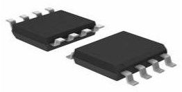
Package
The BSS84LT1G comes in a compact SOT-23 package. This small footprint saves space on printed circuit boards. The SOT-23 package also allows for easy placement in dense layouts, which is helpful in modern home electronics. The package supports surface-mount assembly, making it suitable for both hand-soldering and automated production.
Many hobbyists appreciate the SOT-23 package because it balances size and ease of handling. The leads are accessible for soldering, but the device remains small enough for compact designs. This package choice helps the BSS84LT1G fit into a wide range of home projects, from simple LED drivers to more complex sensor interfaces.
The SOT-23 package ensures that the BSS84LT1G can be used in both prototype and finished products without taking up much space.
onsemi BSS84LT1G in Home Circuits
Low-Power Use
Many home electronics projects require reliable switching for small loads. The onsemi BSS84LT1G performs well in these scenarios. Users often select this MOSFET for controlling indicator LEDs, sensor modules, and miniature relays. The device handles currents up to 130 mA, which covers most low-power applications found in home automation and DIY projects.
In practical tests, the onsemi BSS84LT1G switches LEDs and small relays with ease. The MOSFET responds quickly when connected to microcontroller outputs. This fast response allows for precise timing in circuits that need accurate control. For example, a home automation system can use the BSS84LT1G to turn on a night light or activate a relay for a fan. The device's ability to switch loads instantly ensures smooth operation in these everyday tasks.
Note: The onsemi BSS84LT1G works best when the load current stays below 100 mA. This keeps the device cool and extends its lifespan.
Efficiency
Efficiency matters in home circuits, especially for battery-powered devices. The onsemi BSS84LT1G uses a high cell density process, which enables high-speed switching and low power loss. When a negative voltage appears at the gate, the MOSFET conducts immediately. Removing the gate voltage stops conduction just as quickly. This rapid switching reduces wasted energy and keeps circuits responsive.
The low turn-on resistance of the BSS84LT1G minimizes voltage drop across the device. Less resistance means less heat and higher efficiency. In real-world use, this feature helps maintain battery life in portable gadgets. For example, a wireless sensor node can use the BSS84LT1G to control power to its transmitter. The MOSFET's efficiency ensures the battery lasts longer, even with frequent switching.
| Application | Benefit of BSS84LT1G |
|---|---|
| LED drivers | Low heat, fast response |
| Relay switching | Reliable, efficient |
| Sensor power control | Longer battery life |
Reliability
Reliability stands out as a key strength of the onsemi BSS84LT1G. Users report consistent performance in circuits that switch on and off many times each day. The device maintains stable operation without noticeable degradation, even after thousands of cycles. This reliability makes it a favorite for home automation systems that depend on frequent switching.
Heat management also plays a role in reliability. The BSS84LT1G generates minimal heat during normal operation, which protects nearby components and prevents circuit failures. In repeated tests, the device showed no signs of overheating or instability. Hobbyists and engineers can trust the BSS84LT1G to deliver dependable results in both prototypes and finished products.
🛠️ Tip: For best reliability, avoid exceeding the maximum current rating. Proper layout and soldering also help maintain stable performance over time.
Surprises
Strengths
Many users expect a basic P-channel MOSFET to perform simple switching tasks. The onsemi BSS84LT1G often exceeds these expectations. During hands-on testing, this device shows several unexpected strengths:
Consistent Performance Under Stress
The device maintains stable operation even when switching loads rapidly. In one test, a home automation circuit cycled an LED on and off every second for several days. The MOSFET did not show any sign of failure or heat buildup.Low Heat Generation
Even when driving small relays or multiple LEDs, the device remains cool to the touch. This feature helps protect other components on the circuit board.Direct Logic-Level Control
Many hobbyists find that microcontrollers can drive the gate directly. This removes the need for extra driver circuits. For example, a student project used a microcontroller to control a night light. The onsemi BSS84LT1G switched the light on and off without any glitches.Compact Size, Big Impact
The SOT-23 package fits into tight spaces. Designers can place several MOSFETs on a small board without crowding. This flexibility helps in projects like sensor arrays or compact relay boards.
💡 Tip: The device works best in circuits where the current stays below 100 mA. This keeps the MOSFET efficient and reliable.
Weaknesses
Despite its strengths, the onsemi BSS84LT1G has some limitations that users should consider:
High On-Resistance
The RDS(on) value of about 10 ohms is higher than some other MOSFETs. This resistance can cause a noticeable voltage drop when switching higher currents. In one experiment, a user tried to power a small motor. The voltage drop across the MOSFET reduced the motor speed more than expected.Limited Current Handling
The maximum continuous drain current is 130 mA. This rating restricts the device to low-power applications. If a project needs to switch larger loads, the MOSFET may overheat or fail.Sensitive to Soldering Heat
The small SOT-23 package can be tricky for beginners. Excessive soldering heat may damage the device. One hobbyist reported that the MOSFET stopped working after using a soldering iron for too long on the leads.Not Ideal for High-Speed Switching
While the device switches quickly for most home uses, it may not perform well in circuits that require very fast switching speeds, such as high-frequency PWM motor drivers.
| Scenario | Result with BSS84LT1G | Takeaway |
|---|---|---|
| LED control | Cool, reliable switching | Excellent choice |
| Small relay activation | No heat, stable operation | Very suitable |
| Small motor drive | Noticeable voltage drop | Not recommended |
| High-frequency PWM | Occasional glitches | Use with caution |
⚠️ Note: Always check the current and voltage requirements before choosing this MOSFET for a project.
Alternatives
Comparison
Several P-channel MOSFETs compete with the onsemi BSS84LT1G in home electronics. Designers often compare these devices based on package size, voltage rating, current handling, and on-resistance. The table below highlights some of the most common alternatives:
| Device Name | Manufacturer | Package Types | Notes on Comparison |
|---|---|---|---|
| BSS84LT1G | ON Semiconductor | TO-236-3, SC-59, SOT-23-3 | Reference device for home electronics use |
| NTA4153NT1G | ON Semiconductor | SC-75, SOT-416 | Similar small-signal P-channel MOSFET |
| NVR5198NLT1G | ON Semiconductor | TO-236-3, SC-59, SOT-23-3 | Comparable package and specs |
| NDS355AN | ON Semiconductor | TO-236-3, SC-59, SOT-23-3 | Common alternative in same product category |
| BSS138L | ON Semiconductor | TO-236-3, SC-59, SOT-23-3 | Frequently compared P-channel MOSFET |
| NDS0605 | ON Semiconductor | TO-236-3, SC-59, SOT-23-3 | Similar application and package |
Most alternatives share the SOT-23 package, which saves board space and supports surface-mount assembly. The BSS84LT1G stands out for its balance of voltage rating (50V), moderate current capability (130mA), and reliable switching. Some alternatives, like the NTA4153NT1G, offer similar features but may differ in on-resistance or maximum current. Cost and sourcing remain important factors. The BSS84LT1G is widely available and competitively priced, making it a popular choice for hobbyists and professionals.
📝 Tip: Always check the datasheet for each device. Small differences in on-resistance or current rating can affect circuit performance.
When to Choose
The onsemi BSS84LT1G fits best in projects that need compact size, low power loss, and reliable switching. Its SOT-23 package allows for dense layouts, which helps in modern home electronics. The device handles low-voltage, low-current tasks with ease. Designers often select it for high-side switching or general-purpose low-power control.
Other MOSFETs may offer higher current or voltage ratings, but they often come in larger packages or have higher on-resistance. The BSS84LT1G provides fast switching and low heat generation, which makes it ideal for battery-powered devices and circuits with frequent switching cycles. Many users in online forums choose this MOSFET for its efficiency, reliability, and ease of use in automated assembly.
For projects that require switching small loads, such as LEDs, sensors, or miniature relays, the BSS84LT1G delivers dependable results. When space, efficiency, and simple logic-level control matter most, this device remains a top pick among its peers.
Tips
Best Uses
The onsemi BSS84LT1G works best in low-power switching applications. Many hobbyists use it to control indicator LEDs, small relays, and sensor modules. This MOSFET fits well in battery-powered devices because it generates little heat and uses minimal power. Designers often choose it for high-side switching in home automation systems.
Best practices for using the onsemi BSS84LT1G:
Select this MOSFET for circuits with currents below 100 mA.
Use it in projects where space is limited, such as compact sensor boards.
Pair it with microcontrollers for direct logic-level control.
Apply it in battery-operated gadgets to extend battery life.
💡 Tip: Place the MOSFET close to the load to reduce voltage drop and improve efficiency.
Mistakes
Some users make common mistakes when working with this device. Avoiding these errors helps ensure reliable performance.
Frequent mistakes to watch out for:
Exceeding Current Limits:
Driving loads above 130 mA can cause overheating or device failure.Ignoring On-Resistance:
High RDS(on) may lead to voltage drops, especially with higher currents.Improper Soldering:
Applying too much heat during soldering can damage the SOT-23 package.Incorrect Gate Drive:
Using insufficient gate voltage may prevent the MOSFET from turning on fully.
| Mistake | Impact | Solution |
|---|---|---|
| Overcurrent | Overheating, failure | Stay below 100 mA |
| Poor soldering | Device damage | Use quick, precise solder |
| Low gate voltage | Incomplete switching | Use logic-level drive |
⚠️ Note: Always check the datasheet before adding the MOSFET to a new design.
The onsemi BSS84LT1G delivers more than expected in home electronics. Users see reliable switching, low heat, and easy logic-level control. These strengths make it a smart choice for low-power projects. Hobbyists can trust this device for LED drivers, relay control, and sensor circuits.
Choose the onsemi BSS84LT1G for simple, efficient, and dependable designs.
FAQ
What is the maximum voltage the onsemi BSS84LT1G can handle?
The onsemi BSS84LT1G supports up to -50 volts between drain and source. This rating allows safe use in most low-voltage home circuits.
Can a microcontroller drive the BSS84LT1G directly?
Yes. Most microcontrollers provide enough voltage at the gate to switch the BSS84LT1G fully. No extra driver circuit is needed for typical logic-level signals.
What happens if the current exceeds 130 mA?
Exceeding 130 mA may cause the MOSFET to overheat or fail. Always check the load current before use. Staying below 100 mA improves reliability.
Is the BSS84LT1G suitable for switching motors?
No. The high on-resistance and low current rating make it unsuitable for most motors. Use it for LEDs, relays, or sensors instead.
How should users solder the SOT-23 package safely?
Use a temperature-controlled soldering iron. Limit contact time to a few seconds per lead. This method prevents heat damage and ensures a strong connection.
Specifications
- TypeParameter
- Lifecycle Status
Lifecycle Status refers to the current stage of an electronic component in its product life cycle, indicating whether it is active, obsolete, or transitioning between these states. An active status means the component is in production and available for purchase. An obsolete status indicates that the component is no longer being manufactured or supported, and manufacturers typically provide a limited time frame for support. Understanding the lifecycle status is crucial for design engineers to ensure continuity and reliability in their projects.
ACTIVE (Last Updated: 4 days ago) - Factory Lead Time23 Weeks
- Contact Plating
Contact plating (finish) provides corrosion protection for base metals and optimizes the mechanical and electrical properties of the contact interfaces.
Tin - Mounting Type
The "Mounting Type" in electronic components refers to the method used to attach or connect a component to a circuit board or other substrate, such as through-hole, surface-mount, or panel mount.
Surface Mount - Package / Case
refers to the protective housing that encases an electronic component, providing mechanical support, electrical connections, and thermal management.
TO-236-3, SC-59, SOT-23-3 - Surface Mount
having leads that are designed to be soldered on the side of a circuit board that the body of the component is mounted on.
YES - Number of Pins3
- Transistor Element Material
The "Transistor Element Material" parameter in electronic components refers to the material used to construct the transistor within the component. Transistors are semiconductor devices that amplify or switch electronic signals and are a fundamental building block in electronic circuits. The material used for the transistor element can significantly impact the performance and characteristics of the component. Common materials used for transistor elements include silicon, germanium, and gallium arsenide, each with its own unique properties and suitability for different applications. The choice of transistor element material is crucial in designing electronic components to meet specific performance requirements such as speed, power efficiency, and temperature tolerance.
SILICON - Current - Continuous Drain (Id) @ 25℃130mA Ta
- Drive Voltage (Max Rds On, Min Rds On)5V
- Number of Elements1
- Power Dissipation (Max)225mW Ta
- Turn Off Delay Time
It is the time from when Vgs drops below 90% of the gate drive voltage to when the drain current drops below 90% of the load current. It is the delay before current starts to transition in the load, and depends on Rg. Ciss.
16 ns - Operating Temperature
The operating temperature is the range of ambient temperature within which a power supply, or any other electrical equipment, operate in. This ranges from a minimum operating temperature, to a peak or maximum operating temperature, outside which, the power supply may fail.
-55°C~150°C TJ - Packaging
Semiconductor package is a carrier / shell used to contain and cover one or more semiconductor components or integrated circuits. The material of the shell can be metal, plastic, glass or ceramic.
Cut Tape (CT) - Published2004
- JESD-609 Code
The "JESD-609 Code" in electronic components refers to a standardized marking code that indicates the lead-free solder composition and finish of electronic components for compliance with environmental regulations.
e3 - Pbfree Code
The "Pbfree Code" parameter in electronic components refers to the code or marking used to indicate that the component is lead-free. Lead (Pb) is a toxic substance that has been widely used in electronic components for many years, but due to environmental concerns, there has been a shift towards lead-free alternatives. The Pbfree Code helps manufacturers and users easily identify components that do not contain lead, ensuring compliance with regulations and promoting environmentally friendly practices. It is important to pay attention to the Pbfree Code when selecting electronic components to ensure they meet the necessary requirements for lead-free applications.
yes - Part Status
Parts can have many statuses as they progress through the configuration, analysis, review, and approval stages.
Active - Moisture Sensitivity Level (MSL)
Moisture Sensitivity Level (MSL) is a standardized rating that indicates the susceptibility of electronic components, particularly semiconductors, to moisture-induced damage during storage and the soldering process, defining the allowable exposure time to ambient conditions before they require special handling or baking to prevent failures
1 (Unlimited) - Number of Terminations3
- ECCN Code
An ECCN (Export Control Classification Number) is an alphanumeric code used by the U.S. Bureau of Industry and Security to identify and categorize electronic components and other dual-use items that may require an export license based on their technical characteristics and potential for military use.
EAR99 - Resistance
Resistance is a fundamental property of electronic components that measures their opposition to the flow of electric current. It is denoted by the symbol "R" and is measured in ohms (Ω). Resistance is caused by the collisions of electrons with atoms in a material, which generates heat and reduces the flow of current. Components with higher resistance will impede the flow of current more than those with lower resistance. Resistance plays a crucial role in determining the behavior and functionality of electronic circuits, such as limiting current flow, voltage division, and controlling power dissipation.
10Ohm - Voltage - Rated DC
Voltage - Rated DC is a parameter that specifies the maximum direct current (DC) voltage that an electronic component can safely handle without being damaged. This rating is crucial for ensuring the proper functioning and longevity of the component in a circuit. Exceeding the rated DC voltage can lead to overheating, breakdown, or even permanent damage to the component. It is important to carefully consider this parameter when designing or selecting components for a circuit to prevent any potential issues related to voltage overload.
-50V - Terminal Position
In electronic components, the term "Terminal Position" refers to the physical location of the connection points on the component where external electrical connections can be made. These connection points, known as terminals, are typically used to attach wires, leads, or other components to the main body of the electronic component. The terminal position is important for ensuring proper connectivity and functionality of the component within a circuit. It is often specified in technical datasheets or component specifications to help designers and engineers understand how to properly integrate the component into their circuit designs.
DUAL - Terminal Form
Occurring at or forming the end of a series, succession, or the like; closing; concluding.
GULL WING - Peak Reflow Temperature (Cel)
Peak Reflow Temperature (Cel) is a parameter that specifies the maximum temperature at which an electronic component can be exposed during the reflow soldering process. Reflow soldering is a common method used to attach electronic components to a circuit board. The Peak Reflow Temperature is crucial because it ensures that the component is not damaged or degraded during the soldering process. Exceeding the specified Peak Reflow Temperature can lead to issues such as component failure, reduced performance, or even permanent damage to the component. It is important for manufacturers and assemblers to adhere to the recommended Peak Reflow Temperature to ensure the reliability and functionality of the electronic components.
260 - Current Rating
Current rating is the maximum current that a fuse will carry for an indefinite period without too much deterioration of the fuse element.
-130mA - Time@Peak Reflow Temperature-Max (s)
Time@Peak Reflow Temperature-Max (s) refers to the maximum duration that an electronic component can be exposed to the peak reflow temperature during the soldering process, which is crucial for ensuring reliable solder joint formation without damaging the component.
10 - Pin Count
a count of all of the component leads (or pins)
3 - Element Configuration
The distribution of electrons of an atom or molecule (or other physical structure) in atomic or molecular orbitals.
Single - Operating Mode
A phase of operation during the operation and maintenance stages of the life cycle of a facility.
ENHANCEMENT MODE - Power Dissipation
the process by which an electronic or electrical device produces heat (energy loss or waste) as an undesirable derivative of its primary action.
225mW - Turn On Delay Time
Turn-on delay, td(on), is the time taken to charge the input capacitance of the device before drain current conduction can start.
3.6 ns - FET Type
"FET Type" refers to the type of Field-Effect Transistor (FET) being used in an electronic component. FETs are three-terminal semiconductor devices that can be classified into different types based on their construction and operation. The main types of FETs include Metal-Oxide-Semiconductor FETs (MOSFETs), Junction FETs (JFETs), and Insulated-Gate Bipolar Transistors (IGBTs).Each type of FET has its own unique characteristics and applications. MOSFETs are commonly used in digital circuits due to their high input impedance and low power consumption. JFETs are often used in low-noise amplifiers and switching circuits. IGBTs combine the high input impedance of MOSFETs with the high current-carrying capability of bipolar transistors, making them suitable for high-power applications like motor control and power inverters.When selecting an electronic component, understanding the FET type is crucial as it determines the device's performance and suitability for a specific application. It is important to consider factors such as voltage ratings, current handling capabilities, switching speeds, and power dissipation when choosing the right FET type for a particular circuit design.
P-Channel - Transistor Application
In the context of electronic components, the parameter "Transistor Application" refers to the specific purpose or function for which a transistor is designed and used. Transistors are semiconductor devices that can amplify or switch electronic signals and are commonly used in various electronic circuits. The application of a transistor can vary widely depending on its design and characteristics, such as whether it is intended for audio amplification, digital logic, power control, or radio frequency applications. Understanding the transistor application is important for selecting the right type of transistor for a particular circuit or system to ensure optimal performance and functionality.
SWITCHING - Rds On (Max) @ Id, Vgs
Rds On (Max) @ Id, Vgs refers to the maximum on-resistance of a MOSFET or similar transistor when it is fully turned on or in the saturation region. It is specified at a given drain current (Id) and gate-source voltage (Vgs). This parameter indicates how much resistance the component will offer when conducting, impacting power loss and efficiency in a circuit. Lower Rds On values are preferred for better performance in switching applications.
10 Ω @ 100mA, 5V - Vgs(th) (Max) @ Id
The parameter "Vgs(th) (Max) @ Id" in electronic components refers to the maximum gate-source threshold voltage at a specified drain current (Id). This parameter is commonly found in field-effect transistors (FETs) and is used to define the minimum voltage required at the gate terminal to turn on the transistor and allow current to flow from the drain to the source. The maximum value indicates the upper limit of this threshold voltage under specified operating conditions. It is an important parameter for determining the proper biasing and operating conditions of the FET in a circuit to ensure proper functionality and performance.
2V @ 250μA - Halogen Free
The term "Halogen Free" in electronic components refers to a specific characteristic of the materials used in the manufacturing of the component. Halogens are a group of elements that include fluorine, chlorine, bromine, iodine, and astatine. These elements are commonly used in flame retardants and other materials in electronics. However, the presence of halogens can pose environmental and health risks when the components are disposed of or recycled.Therefore, electronic components labeled as "Halogen Free" are manufactured without the use of halogenated materials. This designation indicates that the components do not contain any halogens, making them safer for the environment and human health. Halogen-free components are becoming increasingly popular in the electronics industry due to the growing awareness of environmental concerns and regulations regarding hazardous substances in electronic products.
Halogen Free - Input Capacitance (Ciss) (Max) @ Vds
The parameter "Input Capacitance (Ciss) (Max) @ Vds" in electronic components refers to the maximum input capacitance measured at a specific drain-source voltage (Vds). Input capacitance is a crucial parameter in field-effect transistors (FETs) and power MOSFETs, as it represents the total capacitance at the input terminal of the device. This capacitance affects the device's switching speed and overall performance, as it influences the time required for charging and discharging during operation. Manufacturers provide this parameter to help designers understand the device's input characteristics and make informed decisions when integrating it into a circuit.
30pF @ 5V - Rise Time
In electronics, when describing a voltage or current step function, rise time is the time taken by a signal to change from a specified low value to a specified high value.
1ns - Vgs (Max)
Vgs (Max) refers to the maximum gate-source voltage that can be applied to a field-effect transistor (FET) without causing damage to the component. This parameter is crucial in determining the safe operating limits of the FET and helps prevent overvoltage conditions that could lead to device failure. Exceeding the specified Vgs (Max) rating can result in breakdown of the gate oxide layer, leading to permanent damage to the FET. Designers must ensure that the applied gate-source voltage does not exceed the maximum rating to ensure reliable and long-term operation of the electronic component.
±20V - Fall Time (Typ)
Fall Time (Typ) is a parameter used to describe the time it takes for a signal to transition from a high level to a low level in an electronic component, such as a transistor or an integrated circuit. It is typically measured in nanoseconds or microseconds and is an important characteristic that affects the performance of the component in digital circuits. A shorter fall time indicates faster switching speeds and can result in improved overall circuit performance, such as reduced power consumption and increased data transmission rates. Designers often consider the fall time specification when selecting components for their circuits to ensure proper functionality and efficiency.
1 ns - Continuous Drain Current (ID)
Continuous Drain Current (ID) is a key parameter in electronic components, particularly in field-effect transistors (FETs) such as MOSFETs. It refers to the maximum current that can flow continuously through the drain terminal of the FET without causing damage to the component. This parameter is crucial for determining the power handling capability of the FET and is specified by the manufacturer in the component's datasheet. Designers must ensure that the actual operating current does not exceed the specified Continuous Drain Current to prevent overheating and potential failure of the component.
130mA - Threshold Voltage
The threshold voltage is a critical parameter in electronic components, particularly in field-effect transistors (FETs). It refers to the minimum voltage required at the input terminal of the FET to turn it on and allow current to flow between the source and drain terminals. Below the threshold voltage, the FET remains in the off state, acting as an open switch. Once the threshold voltage is exceeded, the FET enters the on state, conducting current between the source and drain.The threshold voltage is a key factor in determining the operating characteristics of FETs, such as their switching speed and power consumption. It is typically specified by the manufacturer and can vary depending on the specific type of FET and its design. Designers must consider the threshold voltage when selecting FETs for a particular application to ensure proper functionality and performance.
-2V - Gate to Source Voltage (Vgs)
The Gate to Source Voltage (Vgs) is a crucial parameter in electronic components, particularly in field-effect transistors (FETs) such as MOSFETs. It refers to the voltage difference between the gate and source terminals of the FET. This voltage determines the conductivity of the FET and controls the flow of current through the device. By varying the Vgs, the FET can be switched on or off, allowing for precise control of electronic circuits. Understanding and properly managing the Vgs is essential for ensuring the reliable and efficient operation of FET-based circuits.
20V - Drain to Source Breakdown Voltage
Drain to Source Breakdown Voltage, often denoted as V(BR) D-S, is a critical parameter in electronic components, particularly in field-effect transistors (FETs) and metal-oxide-semiconductor FETs (MOSFETs). It represents the maximum voltage that can be applied between the drain and source terminals of the device without causing breakdown or permanent damage. Exceeding this voltage can lead to excessive current flow, resulting in thermal failure or destruction of the component. It is essential for ensuring reliable operation in circuit designs where high voltages may be encountered.
50V - Nominal Vgs
Nominal Vgs refers to the standard or expected gate-source voltage in field-effect transistors (FETs) and other related electronic components. It represents the voltage level at which the transistor operates optimally, ensuring proper switching characteristics and performance. This parameter is crucial for designers to determine the appropriate control signals required for efficient operation of the device in circuits. Variations from the nominal Vgs can affect the performance and reliability of the component.
2 V - Height1.016mm
- Length3.0226mm
- Width1.397mm
- REACH SVHC
The parameter "REACH SVHC" in electronic components refers to the compliance with the Registration, Evaluation, Authorization, and Restriction of Chemicals (REACH) regulation regarding Substances of Very High Concern (SVHC). SVHCs are substances that may have serious effects on human health or the environment, and their use is regulated under REACH to ensure their safe handling and minimize their impact.Manufacturers of electronic components need to declare if their products contain any SVHCs above a certain threshold concentration and provide information on the safe use of these substances. This information allows customers to make informed decisions about the potential risks associated with using the components and take appropriate measures to mitigate any hazards.Ensuring compliance with REACH SVHC requirements is essential for electronics manufacturers to meet regulatory standards, protect human health and the environment, and maintain transparency in their supply chain. It also demonstrates a commitment to sustainability and responsible manufacturing practices in the electronics industry.
No SVHC - Radiation Hardening
Radiation hardening is the process of making electronic components and circuits resistant to damage or malfunction caused by high levels of ionizing radiation, especially for environments in outer space (especially beyond the low Earth orbit), around nuclear reactors and particle accelerators, or during nuclear accidents or nuclear warfare.
No - RoHS Status
RoHS means “Restriction of Certain Hazardous Substances” in the “Hazardous Substances Directive” in electrical and electronic equipment.
ROHS3 Compliant - Lead Free
Lead Free is a term used to describe electronic components that do not contain lead as part of their composition. Lead is a toxic material that can have harmful effects on human health and the environment, so the electronics industry has been moving towards lead-free components to reduce these risks. Lead-free components are typically made using alternative materials such as silver, copper, and tin. Manufacturers must comply with regulations such as the Restriction of Hazardous Substances (RoHS) directive to ensure that their products are lead-free and environmentally friendly.
Lead Free
Parts with Similar Specs
- ImagePart NumberManufacturerPackage / CaseContinuous Drain Current (ID)Current - Continuous Drain (Id) @ 25°CThreshold VoltageGate to Source Voltage (Vgs)Power DissipationPower Dissipation-MaxRoHS StatusView Compare
![BSS84LT1G]()
BSS84LT1G
TO-236-3, SC-59, SOT-23-3
130 mA
130mA (Ta)
-2 V
20 V
225 mW
225mW (Ta)
ROHS3 Compliant
![2N7002LT3G]()
TO-236-3, SC-59, SOT-23-3
115 mA
115mA (Tc)
1 V
20 V
225 mW
225mW (Ta)
ROHS3 Compliant
![2N7002L]()
TO-236-3, SC-59, SOT-23-3
115 mA
115mA (Tc)
2.5 V
20 V
300 mW
225mW (Ta)
ROHS3 Compliant
![2N7002LT1G]()
TO-236-3, SC-59, SOT-23-3
115 mA
115mA (Ta)
2.5 V
20 V
-
200mW (Ta)
ROHS3 Compliant
![BSS84TA]()
TO-236-3, SC-59, SOT-23-3
130 mA
130mA (Ta)
-
20 V
300 mW
360mW (Ta)
ROHS3 Compliant


Datasheet PDF
- PCN Design/Specification :
- Datasheets :
BSS84LT1G-ON-Semiconductor-datasheet-117484.pdf
BSS84LT1G-ON-Semiconductor-datasheet-94100505.pdf
BSS84LT1G-ON-Semiconductor-datasheet-8537790.pdf
BSS84LT1G-ON-Semiconductor-datasheet-7627526.pdf
BSS84LT1G-ON-Semiconductor-datasheet-14060479.pdf
BSS84LT1G-ON-Semiconductor-datasheet-17590387.pdf
BSS84LT1G-ON-Semiconductor-datasheet-21210845.pdf
BSS84LT1G-ON-Semiconductor-datasheet-9818275.pdf
pid_6384144_bss84lt1g-on-semiconductor-datasheet-139009649.pdf
- PCN Packaging :
- Environmental Information :
- RohsStatement :
 AT89S52 Microcontroller: Application, Pinout and Datasheet
22 September 202116455
 TIP41C Transistor: Datasheet, Pinout, and Test Circuits
09 July 202136043
 A Comprehensive Guide to LTM9008CY-14#PBF 14-Bit Simultaneous Sampling ADC
06 March 2024135
 PL602-21 HCSL Compatible Clock Generator: Pinout, Equivalent and Datasheet
22 February 2022461
 CD4051BE: Featurs, Applications, and Datasheet
08 November 20232045
 UA741CP Operational Amplifier: Pinout, Specification, and Datasheet
18 June 202117217
 UC3844 PWM Controller: Uses, Pinout and Datasheet
11 August 202112932
 2N5458 JFET: Alternatives, Datasheet, Pinout
07 October 20217797
 What is Cat 7 Cable?
04 January 20225823
 STM32U5: The Most Complex Low-power MCU
19 January 20229672
 Automatic Voltage Regulator: Ultimate Guide to Stable Power and Equipment Protection
06 May 20255520
 What is an Encoder?
20 October 20207028
 Development of Ultra-wide Band-gap Ga2O3 Semiconductor Materials in Power MOSFETs
21 October 20223379
 The Understanding to Autonomous Driving Sensor
10 November 20211153
 Introduction to Step-down Transformers
14 October 20207017
 Basic Knowledge of Various Types of Mixers
03 January 20233959
ON Semiconductor
In Stock: 86454
United States
China
Canada
Japan
Russia
Germany
United Kingdom
Singapore
Italy
Hong Kong(China)
Taiwan(China)
France
Korea
Mexico
Netherlands
Malaysia
Austria
Spain
Switzerland
Poland
Thailand
Vietnam
India
United Arab Emirates
Afghanistan
Åland Islands
Albania
Algeria
American Samoa
Andorra
Angola
Anguilla
Antigua & Barbuda
Argentina
Armenia
Aruba
Australia
Azerbaijan
Bahamas
Bahrain
Bangladesh
Barbados
Belarus
Belgium
Belize
Benin
Bermuda
Bhutan
Bolivia
Bonaire, Sint Eustatius and Saba
Bosnia & Herzegovina
Botswana
Brazil
British Indian Ocean Territory
British Virgin Islands
Brunei
Bulgaria
Burkina Faso
Burundi
Cabo Verde
Cambodia
Cameroon
Cayman Islands
Central African Republic
Chad
Chile
Christmas Island
Cocos (Keeling) Islands
Colombia
Comoros
Congo
Congo (DRC)
Cook Islands
Costa Rica
Côte d’Ivoire
Croatia
Cuba
Curaçao
Cyprus
Czechia
Denmark
Djibouti
Dominica
Dominican Republic
Ecuador
Egypt
El Salvador
Equatorial Guinea
Eritrea
Estonia
Eswatini
Ethiopia
Falkland Islands
Faroe Islands
Fiji
Finland
French Guiana
French Polynesia
Gabon
Gambia
Georgia
Ghana
Gibraltar
Greece
Greenland
Grenada
Guadeloupe
Guam
Guatemala
Guernsey
Guinea
Guinea-Bissau
Guyana
Haiti
Honduras
Hungary
Iceland
Indonesia
Iran
Iraq
Ireland
Isle of Man
Israel
Jamaica
Jersey
Jordan
Kazakhstan
Kenya
Kiribati
Kosovo
Kuwait
Kyrgyzstan
Laos
Latvia
Lebanon
Lesotho
Liberia
Libya
Liechtenstein
Lithuania
Luxembourg
Macao(China)
Madagascar
Malawi
Maldives
Mali
Malta
Marshall Islands
Martinique
Mauritania
Mauritius
Mayotte
Micronesia
Moldova
Monaco
Mongolia
Montenegro
Montserrat
Morocco
Mozambique
Myanmar
Namibia
Nauru
Nepal
New Caledonia
New Zealand
Nicaragua
Niger
Nigeria
Niue
Norfolk Island
North Korea
North Macedonia
Northern Mariana Islands
Norway
Oman
Pakistan
Palau
Palestinian Authority
Panama
Papua New Guinea
Paraguay
Peru
Philippines
Pitcairn Islands
Portugal
Puerto Rico
Qatar
Réunion
Romania
Rwanda
Samoa
San Marino
São Tomé & Príncipe
Saudi Arabia
Senegal
Serbia
Seychelles
Sierra Leone
Sint Maarten
Slovakia
Slovenia
Solomon Islands
Somalia
South Africa
South Sudan
Sri Lanka
St Helena, Ascension, Tristan da Cunha
St. Barthélemy
St. Kitts & Nevis
St. Lucia
St. Martin
St. Pierre & Miquelon
St. Vincent & Grenadines
Sudan
Suriname
Svalbard & Jan Mayen
Sweden
Syria
Tajikistan
Tanzania
Timor-Leste
Togo
Tokelau
Tonga
Trinidad & Tobago
Tunisia
Turkey
Turkmenistan
Turks & Caicos Islands
Tuvalu
U.S. Outlying Islands
U.S. Virgin Islands
Uganda
Ukraine
Uruguay
Uzbekistan
Vanuatu
Vatican City
Venezuela
Wallis & Futuna
Yemen
Zambia
Zimbabwe
![2N7002LT1G]() 2N7002LT1G
2N7002LT1GON Semiconductor
![NTA4153NT1G]() NTA4153NT1G
NTA4153NT1GON Semiconductor
![FDB24AN06LA0]() FDB24AN06LA0
FDB24AN06LA0ON Semiconductor
![FDI2532]() FDI2532
FDI2532ON Semiconductor
![FDD16AN08A0-F085]() FDD16AN08A0-F085
FDD16AN08A0-F085ON Semiconductor
![BSS138K]() BSS138K
BSS138KON Semiconductor
![BSS138LT1G]() BSS138LT1G
BSS138LT1GON Semiconductor
![BSS138L]() BSS138L
BSS138LON Semiconductor
![NVR5198NLT1G]() NVR5198NLT1G
NVR5198NLT1GON Semiconductor
![NDS0605]() NDS0605
NDS0605ON Semiconductor


