
 Product
 Brand
Brand Articles
 Tools
Tools
onsemi MMBFJ201 JFET setup, wiring, and tips for audio


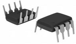
MMBFJ201 Series 40 V 1 mA N-Channel General Purpose Amplifier - SOT-23
Set up the onsemi MMBFJ201 JFET for audio amps: pinout, wiring, biasing, and tips for low-noise, high-fidelity sound in preamps and pedals.
Product Introduction
You can rely on the onsemi mmbfj201 for clean, high-fidelity audio in your next circuit. This N-channel JFET delivers low noise and high input impedance, just like the classic j201 transistor, but in a modern SOT-23 surface-mount package. Many engineers use the onsemi mmbfj201 in audio preamps, pedals, and mixers because it preserves signal quality and supports tube-like tone shaping. Its compact size and reliable performance make it a top choice for today’s audio projects.
Quick Start with onsemi MMBFJ201
Pinout
You will find the onsemi mmbfj201 in a small SOT-23 package. This package has three pins. Each pin connects to a different part of the jfet. The pins are:
| Pin Number | Name | Function |
|---|---|---|
| 1 | Gate | Controls current |
| 2 | Source | Input signal |
| 3 | Drain | Output signal |
When you look at the flat side of the SOT-23 package, pin 1 sits on the left, pin 2 is at the bottom, and pin 3 is on the right. You can use a SOT-23 to DIP adapter if you want to use the onsemi mmbfj201 on a breadboard. This adapter makes it easy to test your jfet before you build a permanent circuit.
Tip: Always double-check the pinout before soldering. Mistakes can damage the jfet or cause the circuit to fail.
Basic Wiring
You can use the onsemi mmbfj201 to build a simple audio preamp. The basic wiring connects the gate to ground through a resistor. The source connects to ground with another resistor. The drain connects to the positive voltage supply through a load resistor. The input signal goes to the gate. The output signal comes from the drain.
Here is a simple schematic for a basic preamp stage:
   +9V
    |
   [Rd]
    |
Drain (3)
    |
   JFET (onsemi mmbfj201)
    |
Source (2)---[Rs]---GND
    |
Gate (1)
    |
   [Rg]
    |
   GND
Input Signal --> Gate (1)
Output Signal <-- Drain (3)
Rd: Drain resistor (usually 10kΩ to 33kΩ)
Rs: Source resistor (usually 1kΩ to 2.2kΩ)
Rg: Gate resistor (usually 1MΩ)
This setup gives you a clean boost for your audio signal.
Setup Steps
You can follow these steps to integrate the onsemi mmbfj201 into your audio circuit:
Identify the SOT-23 package and pinout using the table above.
Solder the mmbfj201 onto a SOT-23 to DIP adapter if you want to use a breadboard.
Place the jfet on your breadboard or PCB.
Connect the gate to ground with a 1MΩ resistor.
Connect the source to ground with a 1kΩ resistor.
Connect the drain to the positive voltage supply through a 10kΩ resistor.
Feed your input signal to the gate.
Take your output signal from the drain.
Power the circuit with 9V DC.
Test the circuit with an audio source and adjust resistor values for best sound.
Note: If you hear distortion or noise, check your wiring and resistor values. Small changes can make a big difference in audio quality.
JFET Wiring Guide
Schematic
You can build a reliable audio preamp using the MMBFJ201 jfet. The following schematic shows a typical setup for boosting a guitar or microphone signal. This design uses common resistor and capacitor values to give you clean sound and low noise.
      +9V
       |
      [Rd] 10kΩ
       |
   Drain (3)
       |
      JFET (MMBFJ201)
       |
Source (2)---[Rs] 1.5kΩ---GND
       |
      [Cs] 10µF
       |
      GND
Gate (1)
       |
      [Rg] 1MΩ
       |
      GND
Input Signal --> Gate (1)
Output Signal <-- Drain (3)
Rd: Drain resistor
Rs: Source resistor
Cs: Source bypass capacitor
Rg: Gate resistor
This schematic helps you understand how each part connects. The input signal enters at the gate. The output comes from the drain. You can change resistor and capacitor values to adjust gain and frequency response.
Tip: Always check the datasheet for the jfet before you build your circuit. The datasheet gives you important details about maximum voltage and current.
Layout Tips
You want your audio project to sound as clean as possible. Good layout helps you reduce noise and interference. Here are some tips for working with the SOT-23 package and different types of boards:
Use a SOT-23 to DIP adapter if you build on a breadboard. This makes the jfet easier to handle.
Keep all signal paths short. Long wires can pick up noise.
Place the input and output wires away from each other. This prevents unwanted feedback.
On perfboard, solder the jfet close to the input jack. This keeps the signal path short.
If you design a PCB, use a solid ground plane under the jfet. This reduces hum and buzz.
Avoid running power traces near the input signal path.
Use shielded cable for input and output if you work in a noisy environment.
Note: Handle the SOT-23 package with care. The small pins can bend easily. Use tweezers and a fine-tip soldering iron for best results.
Power and Bias
The jfet needs the right power and bias to work well in audio circuits. You want stable operation and low noise. Here is what you need to know:
Supply the circuit with a clean 9V DC power source. Batteries work well for portable audio.
The gate of the jfet must stay at 0V (ground) for normal operation.
The source resistor sets the bias current. This current is called idss when vgs equals 0V.
You can adjust the source resistor to set the right vgs. Most audio circuits use a vgs between -0.5V and -1.5V for the MMBFJ201.
The drain resistor sets the output level. You can change this value to get more or less gain.
Add a bypass capacitor across the source resistor if you want higher gain. This lets more signal pass through at higher frequencies.
Alert: If you set the bias wrong, the jfet may distort or cut off the signal. Always measure vgs at the source pin to make sure it is in the right range.
A well-biased jfet gives you stable, low-noise performance. You get the best sound when you match the bias to your specific audio needs.
Audio Performance
Component Values
Choosing the right resistor and capacitor values helps you get the best sound from your small-signal jfet circuit. You want to set the gain and frequency response to match your needs. For most audio preamps, you can start with a 1MΩ resistor from gate to ground. This value keeps the input impedance high. Use a drain resistor between 10kΩ and 33kΩ to set the output level. A source resistor from 1kΩ to 2.2kΩ helps control the bias and gain. If you want more gain at higher frequencies, add a 10µF capacitor across the source resistor. This bypass capacitor boosts the signal without making the sound harsh. Try different values to find the tone you like.
Tip: Write down your resistor and capacitor values as you test them. This helps you remember what works best for your audio project.
Noise Reduction
You want your audio circuit to sound clean and quiet. To reduce noise, keep all wires short and use shielded cables for input and output. Place the small-signal jfet close to the input jack. This keeps the signal path short and lowers the chance of picking up hum or buzz. Use a solid ground connection for all parts. Avoid running power wires near the input. If you use a breadboard, check for loose connections. Good layout and careful wiring make a big difference in noise performance.
Alert: If you hear hiss or hum, check your power supply and ground wiring first.
Stereo Matching
When you build stereo audio circuits, you want both channels to sound the same. You should use two small-signal jfets with similar characteristics. This matching helps keep the gain and tone even in both channels. You can test each jfet with a simple circuit and measure the voltage at the source pin. Pick two devices with close values. This step gives you balanced sound and a better listening experience.
Note: Some suppliers offer matched pairs of jfets for stereo use. This saves you time and gives you reliable results.
Troubleshooting JFET Circuits
Wiring Errors
You might run into problems if you connect the pins incorrectly. Always check the pinout before you start. The SOT-23 package can be tricky because the pins are small and close together. If you use a SOT-23 to DIP adapter, make sure you place the device in the right direction. Double-check your connections for the gate, source, and drain. Sometimes, a loose wire or a cold solder joint can stop your circuit from working. Use a magnifying glass to inspect your work. If you see any solder bridges between pins, remove them with a soldering iron.
Tip: Label your wires or use color-coded jumpers to avoid confusion.
Audio Issues
You may hear unwanted sounds like hum, hiss, or distortion. Hum often comes from poor grounding. Make sure all ground wires connect to a single point. Hiss can happen if you use long wires or if your input cable is not shielded. Distortion usually means the signal is too strong or the bias is not set right. Try lowering the input level or adjusting the source resistor. If the sound is weak, check the drain resistor and make sure your power supply gives a steady voltage.
| Problem | Possible Cause | Solution |
|---|---|---|
| Hum | Bad ground | Use a single ground point |
| Hiss | Long wires, no shield | Shorten wires, use shield |
| Distortion | Wrong bias, high input | Adjust resistor values |
| Weak Output | Low supply, bad drain | Check power, change Rd |
Testing
You can test if your device works by measuring voltages at each pin. Set your multimeter to DC volts. Touch the black probe to ground. Touch the red probe to each pin. The gate should read close to 0V. The source should read between 0.5V and 2V. The drain should read higher, often between 4V and 7V if you use a 9V supply. If you see 0V or 9V at all pins, check your wiring. You can also use an audio probe to listen for signal at the drain. If you hear nothing, the device may be faulty or installed backwards.
Note: Always turn off power before moving wires or changing parts.
Pro Tips for Audio
Tone Shaping
You can use the MMBFJ201 to shape your sound in creative ways. Try changing the source resistor or adding a bypass capacitor. This lets you control the gain and the brightness of your signal. If you want a warmer tone, use a larger source resistor. For a brighter sound, add a small capacitor across the source resistor. You can also build a voltage variable gain stage by connecting a potentiometer in place of the source resistor. This gives you hands-on control over the amount of boost or drive in your audio circuit.
Tip: Experiment with different resistor and capacitor values. Small changes can make a big difference in your final sound.
Integration
You can combine the MMBFJ201 with other parts to build more advanced circuits. Many builders use this JFET as the first stage in an audio limiter circuit. This setup helps protect your speakers from sudden loud sounds. You can also pair the JFET with op-amps to create hybrid preamps. When you add tone controls or filters after the JFET, you get even more options for shaping your sound. Always keep your signal path short and your layout clean for the best results.
| Integration Idea | Benefit |
|---|---|
| Limiter circuit | Protects against peaks |
| Hybrid preamp | Warmer, richer sound |
| Tone control section | Custom sound shaping |
Sourcing
You want to use genuine MMBFJ201 devices for reliable performance. Buy from trusted suppliers or authorized distributors. Check the packaging for the onsemi logo and part number. If you use SOT-23 parts, handle them with care. Use tweezers to pick up the device and a fine-tip soldering iron for mounting. Store unused JFETs in anti-static bags to prevent damage. If you need to test several devices, use a SOT-23 to DIP adapter for easy swapping on your breadboard.
Note: Counterfeit parts can cause noise or failure in your project. Always verify your source before buying.
You can set up the onsemi MMBFJ201 JFET for audio by following clear steps and checking your work. Try different resistor and capacitor values to find your best sound. Watch for these common challenges:
Handle the JFET with static protection.
Match transistors for stereo or critical circuits.
Stay within voltage and current limits.
Checklist:
Double-check pinout and wiring
Use anti-static tools
Test and match devices
Adjust values for tone
Listen and enjoy your results 🎶
Keep exploring new audio ideas with confidence!
FAQ
How do you adapt the onsemi mmbfj201 for breadboard use?
You can use a SOT-23 to DIP adapter. This lets you place the small-signal jfet on a breadboard. Always check the pinout before wiring your circuit. This step helps you avoid mistakes and keeps your audio signal clean.
What is the best way to set the bias for the mmbfj201 in an audio preamp?
You set the bias by choosing the right source resistor. Measure vgs at the source pin. Aim for a vgs between -0.5V and -1.5V. This gives you stable idss and low noise in your audio circuit.
Can you use the mmbfj201 as a replacement for the j201 transistor in a schematic?
Yes, you can use the mmbfj201 as a modern replacement for the j201 transistor. The onsemi mmbfj201 works well in most audio circuits. Always check the schematic and adjust resistor values for best performance.
How do you reduce noise in a small-signal jfet audio circuit?
Keep all wires short. Use shielded cables for input and output. Place the jfet close to the input jack. Good layout and solid ground connections help you get a quiet audio signal.
What is a voltage variable gain stage and how does it help in audio?
A voltage variable gain stage lets you control the gain of your audio signal. You can use a potentiometer in the source leg of the mmbfj201. This setup gives you hands-on control over the boost in your audio limiter circuit.
Specifications
- TypeParameter
- Lifecycle Status
Lifecycle Status refers to the current stage of an electronic component in its product life cycle, indicating whether it is active, obsolete, or transitioning between these states. An active status means the component is in production and available for purchase. An obsolete status indicates that the component is no longer being manufactured or supported, and manufacturers typically provide a limited time frame for support. Understanding the lifecycle status is crucial for design engineers to ensure continuity and reliability in their projects.
ACTIVE (Last Updated: 12 hours ago) - Factory Lead Time42 Weeks
- Mount
In electronic components, the term "Mount" typically refers to the method or process of physically attaching or fixing a component onto a circuit board or other electronic device. This can involve soldering, adhesive bonding, or other techniques to secure the component in place. The mounting process is crucial for ensuring proper electrical connections and mechanical stability within the electronic system. Different components may have specific mounting requirements based on their size, shape, and function, and manufacturers provide guidelines for proper mounting procedures to ensure optimal performance and reliability of the electronic device.
Surface Mount - Mounting Type
The "Mounting Type" in electronic components refers to the method used to attach or connect a component to a circuit board or other substrate, such as through-hole, surface-mount, or panel mount.
Surface Mount - Package / Case
refers to the protective housing that encases an electronic component, providing mechanical support, electrical connections, and thermal management.
TO-236-3, SC-59, SOT-23-3 - Number of Pins3
- Weight30mg
- Transistor Element Material
The "Transistor Element Material" parameter in electronic components refers to the material used to construct the transistor within the component. Transistors are semiconductor devices that amplify or switch electronic signals and are a fundamental building block in electronic circuits. The material used for the transistor element can significantly impact the performance and characteristics of the component. Common materials used for transistor elements include silicon, germanium, and gallium arsenide, each with its own unique properties and suitability for different applications. The choice of transistor element material is crucial in designing electronic components to meet specific performance requirements such as speed, power efficiency, and temperature tolerance.
SILICON - Breakdown Voltage / V-40V
- Number of Elements1
- Operating Temperature
The operating temperature is the range of ambient temperature within which a power supply, or any other electrical equipment, operate in. This ranges from a minimum operating temperature, to a peak or maximum operating temperature, outside which, the power supply may fail.
-55°C~150°C TJ - Packaging
Semiconductor package is a carrier / shell used to contain and cover one or more semiconductor components or integrated circuits. The material of the shell can be metal, plastic, glass or ceramic.
Tape & Reel (TR) - Published2008
- JESD-609 Code
The "JESD-609 Code" in electronic components refers to a standardized marking code that indicates the lead-free solder composition and finish of electronic components for compliance with environmental regulations.
e3 - Pbfree Code
The "Pbfree Code" parameter in electronic components refers to the code or marking used to indicate that the component is lead-free. Lead (Pb) is a toxic substance that has been widely used in electronic components for many years, but due to environmental concerns, there has been a shift towards lead-free alternatives. The Pbfree Code helps manufacturers and users easily identify components that do not contain lead, ensuring compliance with regulations and promoting environmentally friendly practices. It is important to pay attention to the Pbfree Code when selecting electronic components to ensure they meet the necessary requirements for lead-free applications.
yes - Part Status
Parts can have many statuses as they progress through the configuration, analysis, review, and approval stages.
Active - Moisture Sensitivity Level (MSL)
Moisture Sensitivity Level (MSL) is a standardized rating that indicates the susceptibility of electronic components, particularly semiconductors, to moisture-induced damage during storage and the soldering process, defining the allowable exposure time to ambient conditions before they require special handling or baking to prevent failures
1 (Unlimited) - Number of Terminations3
- ECCN Code
An ECCN (Export Control Classification Number) is an alphanumeric code used by the U.S. Bureau of Industry and Security to identify and categorize electronic components and other dual-use items that may require an export license based on their technical characteristics and potential for military use.
EAR99 - Terminal Finish
Terminal Finish refers to the surface treatment applied to the terminals or leads of electronic components to enhance their performance and longevity. It can improve solderability, corrosion resistance, and overall reliability of the connection in electronic assemblies. Common finishes include nickel, gold, and tin, each possessing distinct properties suitable for various applications. The choice of terminal finish can significantly impact the durability and effectiveness of electronic devices.
Tin (Sn) - Voltage - Rated DC
Voltage - Rated DC is a parameter that specifies the maximum direct current (DC) voltage that an electronic component can safely handle without being damaged. This rating is crucial for ensuring the proper functioning and longevity of the component in a circuit. Exceeding the rated DC voltage can lead to overheating, breakdown, or even permanent damage to the component. It is important to carefully consider this parameter when designing or selecting components for a circuit to prevent any potential issues related to voltage overload.
40V - Max Power Dissipation
The maximum power that the MOSFET can dissipate continuously under the specified thermal conditions.
350mW - Terminal Position
In electronic components, the term "Terminal Position" refers to the physical location of the connection points on the component where external electrical connections can be made. These connection points, known as terminals, are typically used to attach wires, leads, or other components to the main body of the electronic component. The terminal position is important for ensuring proper connectivity and functionality of the component within a circuit. It is often specified in technical datasheets or component specifications to help designers and engineers understand how to properly integrate the component into their circuit designs.
DUAL - Terminal Form
Occurring at or forming the end of a series, succession, or the like; closing; concluding.
GULL WING - Current Rating
Current rating is the maximum current that a fuse will carry for an indefinite period without too much deterioration of the fuse element.
50mA - Base Part Number
The "Base Part Number" (BPN) in electronic components serves a similar purpose to the "Base Product Number." It refers to the primary identifier for a component that captures the essential characteristics shared by a group of similar components. The BPN provides a fundamental way to reference a family or series of components without specifying all the variations and specific details.
MBFJ201 - Number of Channels1
- Element Configuration
The distribution of electrons of an atom or molecule (or other physical structure) in atomic or molecular orbitals.
Single - Operating Mode
A phase of operation during the operation and maintenance stages of the life cycle of a facility.
DEPLETION MODE - Power Dissipation
the process by which an electronic or electrical device produces heat (energy loss or waste) as an undesirable derivative of its primary action.
350mW - FET Type
"FET Type" refers to the type of Field-Effect Transistor (FET) being used in an electronic component. FETs are three-terminal semiconductor devices that can be classified into different types based on their construction and operation. The main types of FETs include Metal-Oxide-Semiconductor FETs (MOSFETs), Junction FETs (JFETs), and Insulated-Gate Bipolar Transistors (IGBTs).Each type of FET has its own unique characteristics and applications. MOSFETs are commonly used in digital circuits due to their high input impedance and low power consumption. JFETs are often used in low-noise amplifiers and switching circuits. IGBTs combine the high input impedance of MOSFETs with the high current-carrying capability of bipolar transistors, making them suitable for high-power applications like motor control and power inverters.When selecting an electronic component, understanding the FET type is crucial as it determines the device's performance and suitability for a specific application. It is important to consider factors such as voltage ratings, current handling capabilities, switching speeds, and power dissipation when choosing the right FET type for a particular circuit design.
N-Channel - Transistor Application
In the context of electronic components, the parameter "Transistor Application" refers to the specific purpose or function for which a transistor is designed and used. Transistors are semiconductor devices that can amplify or switch electronic signals and are commonly used in various electronic circuits. The application of a transistor can vary widely depending on its design and characteristics, such as whether it is intended for audio amplification, digital logic, power control, or radio frequency applications. Understanding the transistor application is important for selecting the right type of transistor for a particular circuit or system to ensure optimal performance and functionality.
AMPLIFIER - Drain to Source Voltage (Vdss)
The Drain to Source Voltage (Vdss) is a key parameter in electronic components, particularly in field-effect transistors (FETs) such as MOSFETs. It refers to the maximum voltage that can be applied between the drain and source terminals of the FET without causing damage to the component. Exceeding this voltage limit can lead to breakdown and potentially permanent damage to the device.Vdss is an important specification to consider when designing or selecting components for a circuit, as it determines the operating range and reliability of the FET. It is crucial to ensure that the Vdss rating of the component is higher than the maximum voltage expected in the circuit to prevent failures and ensure proper functionality.In summary, the Drain to Source Voltage (Vdss) is a critical parameter that defines the maximum voltage tolerance of a FET component and plays a significant role in determining the overall performance and reliability of electronic circuits.
40V - Continuous Drain Current (ID)
Continuous Drain Current (ID) is a key parameter in electronic components, particularly in field-effect transistors (FETs) such as MOSFETs. It refers to the maximum current that can flow continuously through the drain terminal of the FET without causing damage to the component. This parameter is crucial for determining the power handling capability of the FET and is specified by the manufacturer in the component's datasheet. Designers must ensure that the actual operating current does not exceed the specified Continuous Drain Current to prevent overheating and potential failure of the component.
1mA - Gate to Source Voltage (Vgs)
The Gate to Source Voltage (Vgs) is a crucial parameter in electronic components, particularly in field-effect transistors (FETs) such as MOSFETs. It refers to the voltage difference between the gate and source terminals of the FET. This voltage determines the conductivity of the FET and controls the flow of current through the device. By varying the Vgs, the FET can be switched on or off, allowing for precise control of electronic circuits. Understanding and properly managing the Vgs is essential for ensuring the reliable and efficient operation of FET-based circuits.
-40V - FET Technology
Field-Effect Transistor (FET) technology is a type of semiconductor device commonly used in electronic components such as transistors and integrated circuits. FETs operate by controlling the flow of current through a semiconductor channel using an electric field. There are several types of FETs, including Metal-Oxide-Semiconductor FETs (MOSFETs) and Junction FETs (JFETs), each with its own characteristics and applications. FET technology offers advantages such as high input impedance, low power consumption, and fast switching speeds, making it suitable for a wide range of electronic devices and circuits. Overall, FET technology plays a crucial role in modern electronics by enabling efficient and reliable signal processing and amplification.
JUNCTION - Max Junction Temperature (Tj)
Max Junction Temperature (Tj) refers to the maximum allowable temperature at the junction of a semiconductor device, such as a transistor or integrated circuit. It is a critical parameter that influences the performance, reliability, and lifespan of the component. Exceeding this temperature can lead to thermal runaway, breakdown, or permanent damage to the device. Proper thermal management is essential to ensure the junction temperature remains within safe operating limits during device operation.
150°C - Current - Drain (Idss) @ Vds (Vgs=0)
The parameter "Current - Drain (Idss) @ Vds (Vgs=0)" in electronic components refers to the maximum drain current that flows through the device when the gate-source voltage (Vgs) is zero. This parameter is typically specified for field-effect transistors (FETs) and is an important characteristic that indicates the device's maximum current-carrying capacity in the off state. It helps in determining the saturation current of the FET and is crucial for designing circuits where high current handling capability is required. Manufacturers provide this parameter in the datasheet of the component to assist engineers and designers in selecting the appropriate component for their applications.
200μA @ 20V - Voltage - Cutoff (VGS off) @ Id
Voltage - Cutoff (VGS off) @ Id refers to the gate-source voltage at which a field-effect transistor (FET) or similar device ceases to conduct, effectively turning it off. This parameter indicates the threshold voltage that separates the conducting state from the cutoff state for a specified drain current (Id). It is crucial for determining the operating characteristics of the device in various applications, ensuring efficient switching and control in electronic circuits.
300mV @ 10nA - Height1.2mm
- Length2.92mm
- Width1.3mm
- REACH SVHC
The parameter "REACH SVHC" in electronic components refers to the compliance with the Registration, Evaluation, Authorization, and Restriction of Chemicals (REACH) regulation regarding Substances of Very High Concern (SVHC). SVHCs are substances that may have serious effects on human health or the environment, and their use is regulated under REACH to ensure their safe handling and minimize their impact.Manufacturers of electronic components need to declare if their products contain any SVHCs above a certain threshold concentration and provide information on the safe use of these substances. This information allows customers to make informed decisions about the potential risks associated with using the components and take appropriate measures to mitigate any hazards.Ensuring compliance with REACH SVHC requirements is essential for electronics manufacturers to meet regulatory standards, protect human health and the environment, and maintain transparency in their supply chain. It also demonstrates a commitment to sustainability and responsible manufacturing practices in the electronics industry.
No SVHC - Radiation Hardening
Radiation hardening is the process of making electronic components and circuits resistant to damage or malfunction caused by high levels of ionizing radiation, especially for environments in outer space (especially beyond the low Earth orbit), around nuclear reactors and particle accelerators, or during nuclear accidents or nuclear warfare.
No - RoHS Status
RoHS means “Restriction of Certain Hazardous Substances” in the “Hazardous Substances Directive” in electrical and electronic equipment.
ROHS3 Compliant - Lead Free
Lead Free is a term used to describe electronic components that do not contain lead as part of their composition. Lead is a toxic material that can have harmful effects on human health and the environment, so the electronics industry has been moving towards lead-free components to reduce these risks. Lead-free components are typically made using alternative materials such as silver, copper, and tin. Manufacturers must comply with regulations such as the Restriction of Hazardous Substances (RoHS) directive to ensure that their products are lead-free and environmentally friendly.
Lead Free
Parts with Similar Specs
- ImagePart NumberManufacturerMountPackage / CaseDrain to Source Voltage (Vdss)Continuous Drain Current (ID)Max Power DissipationPower DissipationGate to Source Voltage (Vgs)Number of TerminationsView Compare
![MMBFJ201]()
MMBFJ201
Surface Mount
TO-236-3, SC-59, SOT-23-3
40 V
1 mA
350 mW
350 mW
-40 V
3
![MMBF4092]()
Surface Mount
TO-236-3, SC-59, SOT-23-3
40 V
30 mA
350 mW
350 mW
-40 V
3
![MMBF4091]()
Surface Mount
TO-236-3, SC-59, SOT-23-3
40 V
15 mA
350 mW
350 mW
-40 V
3
![MMBF5103]()
Surface Mount
TO-236-3, SC-59, SOT-23-3
40 V
40 mA
350 mW
350 mW
-40 V
3
![PMBF4391,215]()
-
TO-236-3, SC-59, SOT-23-3
-
-
-
-
-
3


Datasheet PDF
- PCN Design/Specification :
- Datasheets :
- PCN Assembly/Origin :
- Environmental Information :
- PCN Packaging :
 A Comprehensive Guide to Tamura 2DM150806CM Gate Driver
11 March 20241049
 H6 vs H7 Battery: Which One Do You Like Better?
01 April 202247337
 LM393P Dual Comparator: 36V, Pinout, Datasheet
17 March 20226737
![NE555 VS TS555 Power Consumption[Video]](https://res.utmel.com/Images/Article/eba3ee53-0b70-41c0-b54a-9fb20bd06422.png) NE555 VS TS555 Power Consumption[Video]
NE555 VS TS555 Power Consumption[Video]25 April 20222934
 LME49720 Audio Operational Amplifier: Circuit, Price and Alternatives
29 June 20214971
 ADG1414 SPST Switches: Pinout, Features and Datasheet
15 February 20222295
 TL074 OP-AMP: Pinout, Datasheet and TL074 vs. TL084
16 November 202116726
 AD620 Instrumentation Amplifier: Pinout, Schematic and Price
30 July 20217501
 The History of Microscope
21 October 20217451
 Rectangular Connectors vs Circular Connectors: Which fits your Project Best
04 July 20252055
 Review of IoT-Based Smart Home Security Systems- Part 1
28 March 20243655
![How a CPU is made? [HD Graphics]](https://res.utmel.com/Images/Article/d7470283-3897-4776-abd1-e7eef60aff17.jpg) How a CPU is made? [HD Graphics]
How a CPU is made? [HD Graphics]07 January 202615557
 Latches, Flip-Flops, Registers and Buffers
15 February 202216633
 Hot Swap Controllers:Semiconductors That Provide In-circuit Protection and Control Functions
22 February 20234213
 What is ISP (Image Signal Processor)?
15 September 202135392
 What is Bluetooth Low Energy (BLE) Audio Technology?
26 April 20226358
ON Semiconductor
In Stock: 2885
United States
China
Canada
Japan
Russia
Germany
United Kingdom
Singapore
Italy
Hong Kong(China)
Taiwan(China)
France
Korea
Mexico
Netherlands
Malaysia
Austria
Spain
Switzerland
Poland
Thailand
Vietnam
India
United Arab Emirates
Afghanistan
Åland Islands
Albania
Algeria
American Samoa
Andorra
Angola
Anguilla
Antigua & Barbuda
Argentina
Armenia
Aruba
Australia
Azerbaijan
Bahamas
Bahrain
Bangladesh
Barbados
Belarus
Belgium
Belize
Benin
Bermuda
Bhutan
Bolivia
Bonaire, Sint Eustatius and Saba
Bosnia & Herzegovina
Botswana
Brazil
British Indian Ocean Territory
British Virgin Islands
Brunei
Bulgaria
Burkina Faso
Burundi
Cabo Verde
Cambodia
Cameroon
Cayman Islands
Central African Republic
Chad
Chile
Christmas Island
Cocos (Keeling) Islands
Colombia
Comoros
Congo
Congo (DRC)
Cook Islands
Costa Rica
Côte d’Ivoire
Croatia
Cuba
Curaçao
Cyprus
Czechia
Denmark
Djibouti
Dominica
Dominican Republic
Ecuador
Egypt
El Salvador
Equatorial Guinea
Eritrea
Estonia
Eswatini
Ethiopia
Falkland Islands
Faroe Islands
Fiji
Finland
French Guiana
French Polynesia
Gabon
Gambia
Georgia
Ghana
Gibraltar
Greece
Greenland
Grenada
Guadeloupe
Guam
Guatemala
Guernsey
Guinea
Guinea-Bissau
Guyana
Haiti
Honduras
Hungary
Iceland
Indonesia
Iran
Iraq
Ireland
Isle of Man
Israel
Jamaica
Jersey
Jordan
Kazakhstan
Kenya
Kiribati
Kosovo
Kuwait
Kyrgyzstan
Laos
Latvia
Lebanon
Lesotho
Liberia
Libya
Liechtenstein
Lithuania
Luxembourg
Macao(China)
Madagascar
Malawi
Maldives
Mali
Malta
Marshall Islands
Martinique
Mauritania
Mauritius
Mayotte
Micronesia
Moldova
Monaco
Mongolia
Montenegro
Montserrat
Morocco
Mozambique
Myanmar
Namibia
Nauru
Nepal
New Caledonia
New Zealand
Nicaragua
Niger
Nigeria
Niue
Norfolk Island
North Korea
North Macedonia
Northern Mariana Islands
Norway
Oman
Pakistan
Palau
Palestinian Authority
Panama
Papua New Guinea
Paraguay
Peru
Philippines
Pitcairn Islands
Portugal
Puerto Rico
Qatar
Réunion
Romania
Rwanda
Samoa
San Marino
São Tomé & Príncipe
Saudi Arabia
Senegal
Serbia
Seychelles
Sierra Leone
Sint Maarten
Slovakia
Slovenia
Solomon Islands
Somalia
South Africa
South Sudan
Sri Lanka
St Helena, Ascension, Tristan da Cunha
St. Barthélemy
St. Kitts & Nevis
St. Lucia
St. Martin
St. Pierre & Miquelon
St. Vincent & Grenadines
Sudan
Suriname
Svalbard & Jan Mayen
Sweden
Syria
Tajikistan
Tanzania
Timor-Leste
Togo
Tokelau
Tonga
Trinidad & Tobago
Tunisia
Turkey
Turkmenistan
Turks & Caicos Islands
Tuvalu
U.S. Outlying Islands
U.S. Virgin Islands
Uganda
Ukraine
Uruguay
Uzbekistan
Vanuatu
Vatican City
Venezuela
Wallis & Futuna
Yemen
Zambia
Zimbabwe
![MMBFJ177LT1G]() MMBFJ177LT1G
MMBFJ177LT1GON Semiconductor
![MMBFJ108]() MMBFJ108
MMBFJ108ON Semiconductor
![MMBF4391LT1G]() MMBF4391LT1G
MMBF4391LT1GON Semiconductor
![MMBF4393LT1G]() MMBF4393LT1G
MMBF4393LT1GON Semiconductor
![MMBFJ175]() MMBFJ175
MMBFJ175ON Semiconductor
![MMBFJ175LT1G]() MMBFJ175LT1G
MMBFJ175LT1GON Semiconductor
![MMBF4392LT1G]() MMBF4392LT1G
MMBF4392LT1GON Semiconductor
![MMBFJ202]() MMBFJ202
MMBFJ202ON Semiconductor
![J175-D26Z]() J175-D26Z
J175-D26ZON Semiconductor


