
 Product
 Brand
Brand Articles
 Tools
Tools
8533AG-01 LVPECL Fanout Buffer: Pinout, Features and Datasheet

Renesas Electronics America Inc.
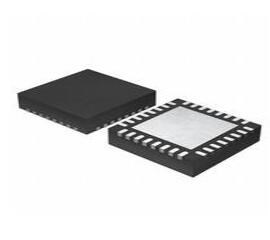
1 Circuit 2:4 Clock Buffer ICS8533-01 20-TSSOP (0.173, 4.40mm Width)
Unit Price: $11.514352
Ext Price: $11.51


1 Circuit 2:4 Clock Buffer ICS8533-01 20-TSSOP (0.173, 4.40mm Width)
The 8533AG-01 is a low skew, high performance 1-to-4 Differential-to-3.3V LVPECL Fanout Buffer. The 8533AG-01 has two selectable clock inputs. Guaranteed output and part-to-part skew characteristics make the 8533AG-01 ideal for those applications demanding well defined performance and repeatability. Furthermore, Huge range of Semiconductors, Capacitors, Resistors and IcS in stock. Welcome RFQ.
8533AG-01 Pinout
The following figure is the diagram of 8533AG-01 Pinout.

Pinout
8533AG-01 CAD Model
The followings are 8533AG-01 Symbol, Footprint, and 3D Model.

PCB Symbol

PCB Footprint

3D Model
8533AG-01 Overview
The 8533AG-01 is a low skew, high performance 1-to-4 Differential-to-3.3V LVPECL Fanout Buffer. The 8533AG-01 has two selectable clock inputs. The CLK, nCLK pair can accept most standard differential input levels. The PCLK, nPCLK pair can accept LVPECL, CML, or SSTL input levels. The clock enable is internally synchronized to eliminate runt pulses on the outputs during asynchronous assertion/deassertion of the clock enable pin. Guaranteed output and part-to-part skew characteristics make the 8533AG-01 ideal for those applications demanding well defined performance and repeatability.
This article provides you with a basic overview of the 8533AG-01 LVPECL Fanout Buffer, including its pin descriptions, features and specifications, etc., to help you quickly understand what 8533AG-01 is.
8533AG-01 Features
● Four differential 3.3V LVPECL outputs
● Selectable differential CLK, nCLK or LVPECL clock inputs
● CLK, nCLK pair can accept the following differential input levels: LVDS, LVPECL, LVHSTL, SSTL, HCSL
● PCLK, nPCLK supports the following input types: LVPECL, CML, SSTL
● Maximum output frequency: 650MHz
● Translates any single-ended input signal to 3.3V LVPECL levels with resistor bias on nCLK input
● Output skew: 30ps (maximum)
● Part-to-part skew: 150ps (maximum)
● Propagation delay: 1.4ns (maximum)
● Additive phase jitter, RMS: 0.06ps (typical)
● 3.3V operating supply
● 0°C to 70°C ambient operating temperature
● Lead-Free package
● Industrial temperature information available upon request
Specifications
- TypeParameter
- Factory Lead Time12 Weeks
- Mounting Type
The "Mounting Type" in electronic components refers to the method used to attach or connect a component to a circuit board or other substrate, such as through-hole, surface-mount, or panel mount.
Surface Mount - Package / Case
refers to the protective housing that encases an electronic component, providing mechanical support, electrical connections, and thermal management.
20-TSSOP (0.173, 4.40mm Width) - Frequency(Max)650MHz
- Operating Temperature
The operating temperature is the range of ambient temperature within which a power supply, or any other electrical equipment, operate in. This ranges from a minimum operating temperature, to a peak or maximum operating temperature, outside which, the power supply may fail.
0°C~70°C - Packaging
Semiconductor package is a carrier / shell used to contain and cover one or more semiconductor components or integrated circuits. The material of the shell can be metal, plastic, glass or ceramic.
Tube - Part Status
Parts can have many statuses as they progress through the configuration, analysis, review, and approval stages.
Active - Moisture Sensitivity Level (MSL)
Moisture Sensitivity Level (MSL) is a standardized rating that indicates the susceptibility of electronic components, particularly semiconductors, to moisture-induced damage during storage and the soldering process, defining the allowable exposure time to ambient conditions before they require special handling or baking to prevent failures
1 (Unlimited) - TypeFanout Buffer (Distribution), Multiplexer
- Voltage - Supply
Voltage - Supply refers to the range of voltage levels that an electronic component or circuit is designed to operate with. It indicates the minimum and maximum supply voltage that can be applied for the device to function properly. Providing supply voltages outside this range can lead to malfunction, damage, or reduced performance. This parameter is critical for ensuring compatibility between different components in a circuit.
3.135V~3.465V - Base Part Number
The "Base Part Number" (BPN) in electronic components serves a similar purpose to the "Base Product Number." It refers to the primary identifier for a component that captures the essential characteristics shared by a group of similar components. The BPN provides a fundamental way to reference a family or series of components without specifying all the variations and specific details.
ICS8533-01 - Output
In electronic components, the parameter "Output" typically refers to the signal or data that is produced by the component and sent to another part of the circuit or system. The output can be in the form of voltage, current, frequency, or any other measurable quantity depending on the specific component. The output of a component is often crucial in determining its functionality and how it interacts with other components in the circuit. Understanding the output characteristics of electronic components is essential for designing and troubleshooting electronic circuits effectively.
LVPECL - Number of Circuits1
- Input
In electronic components, "Input" refers to the signal or data that is provided to a device or system for processing or manipulation. It is the information or command that is received by the component to initiate a specific function or operation. The input can come from various sources such as sensors, other electronic devices, or user interactions. It is crucial for the proper functioning of the component as it determines how the device will respond or behave based on the input received. Understanding and managing the input parameters is essential in designing and using electronic components effectively.
CML, HCSL, LVDS, LVHSTL, LVPECL, SSTL - Ratio - Input:Output
The parameter "Ratio - Input:Output" in electronic components refers to the relationship between the input and output quantities of a device or system. It is a measure of how the input signal or energy is transformed or converted into the output signal or energy. This ratio is often expressed as a numerical value or percentage, indicating the efficiency or effectiveness of the component in converting the input to the desired output. A higher ratio typically signifies better performance or higher efficiency, while a lower ratio may indicate losses or inefficiencies in the conversion process. Understanding and optimizing the input-output ratio is crucial in designing and evaluating electronic components for various applications.
2:4 - Differential - Input:Output
Differential - Input:Output refers to the relationship between the input and output signals in differential amplifiers or circuits. It measures the difference in voltage between two input terminals and produces an output that is proportional to this difference. This parameter is essential for noise rejection and improving signal integrity in various applications, such as operational amplifiers and data acquisition systems. It allows circuits to effectively amplify small signals while minimizing interference and common-mode noise.
Yes/Yes - RoHS Status
RoHS means “Restriction of Certain Hazardous Substances” in the “Hazardous Substances Directive” in electrical and electronic equipment.
ROHS3 Compliant
8533AG-01 Functional Block Diagram
The following is the Block Diagram of 8533AG-01.

Block Diagram
8533AG-01 Package
The following diagram shows the 8533AG-01 Package.

Package
8533AG-01 Manufacturer
Renesas Electronics delivers trusted embedded design innovation with complete semiconductor solutions that enable billions of connected, intelligent devices to enhance the way people work and live - securely and safely.The number one global supplier of microcontrollers, and a leader in Analog & Power and SoC products, Renesas provides the expertise, quality, and comprehensive solutions for a broad range of Automotive, Industrial, Home Electronics (HE), Office Automation (OA) and Information Communication Technology (ICT) applications to help shape a limitless future.
Datasheet PDF
- PCN Design/Specification :
- PCN Assembly/Origin :
- Datasheets :
How many pins of 8533AG-01LF?
20 Pins.
What’s the operating temperature of 8533AG-01LF?
0°C~70°C.
What is the essential property of the 8533AG-01?
The 8533AG-01 is a low skew, high performance 1-to-4 Differential-to-3.3V LVPECL Fanout Buffer. The 8533AG-01 has two selectable clock inputs.
 EFM32TG Microcontroller: Datasheet, Pinout and Application
14 July 2021969
 AO4407A 30V P-Channel MOSFET, 12A 8SOIC and AO4407A Equivalents
07 February 20229398
 TIP29C Transistor: Where & How to Use?
11 November 20212468
 CR2025 Battery: Features, Pinout, and Datasheet
30 September 20213862
 ATECC608A IC: Datasheet, Pinout and Application
05 August 20219504
 ULN2803A Transistor Array: Pinout, Circuit, and Datasheet
15 June 202119120
 Decoding the Microchip PIC16F5X Series: Flash-Based 8-Bit CMOS Microcontrollers
29 February 2024191
 MLX90614 Infra Red Thermometer: Pinout, Datasheet and Applications
30 July 20216484
 Cellular IoT Transmit Module for Enhanced Connectivity and Power Efficiency with Extended Battery Life
30 January 20242191
 Effect Of Target Physical Properties And Energetic Ions When Doping Thin-Body Semiconductor
19 October 20222419
 Analysis of Common Misunderstandings of Isolation Technology
25 April 20225345
 50 Frequently Asked Questions about Oscilloscope
22 November 202112129
 Semiconductor Industry's Uphill Battle Towards Net Zero
22 September 20232042
 The Era of UFS 4.0, Announced?
06 May 20226645
 HIKSEMI Authorized Distributor | UTMEL Electronics
15 November 20233659
 Semiconductor Inspection System Market Expected to Reach US$ 8,380.01 Million By 2030
15 September 20233658
Renesas Electronics America Inc.
In Stock: 444
Minimum: 1 Multiples: 1
Qty
Unit Price
Ext Price
1
$11.514352
$11.51
10
$10.862596
$108.63
100
$10.247732
$1,024.77
500
$9.667672
$4,833.84
1000
$9.120445
$9,120.44
Not the price you want? Send RFQ Now and we'll contact you ASAP.
Inquire for More Quantity
![49FCT3805PYGI]() 49FCT3805PYGI
49FCT3805PYGIRenesas Electronics America Inc.
![LV810FILFT]() LV810FILFT
LV810FILFTRenesas Electronics America Inc.
![49FCT3805AQG8]() 49FCT3805AQG8
49FCT3805AQG8Renesas Electronics America Inc.
![553MLFT]() 553MLFT
553MLFTRenesas Electronics America Inc.
![83905AGLFT]() 83905AGLFT
83905AGLFTRenesas Electronics America Inc.
![49FCT3805APYG8]() 49FCT3805APYG8
49FCT3805APYG8Renesas Electronics America Inc.
![74FCT3807AQG8]() 74FCT3807AQG8
74FCT3807AQG8Renesas Electronics America Inc.
![49FCT3805DQGI8]() 49FCT3805DQGI8
49FCT3805DQGI8Renesas Electronics America Inc.
![49FCT3805APYGI8]() 49FCT3805APYGI8
49FCT3805APYGI8Renesas Electronics America Inc.
![74FCT3807DQGI8]() 74FCT3807DQGI8
74FCT3807DQGI8Renesas Electronics America Inc.


