
 Product
 Brand
Brand Articles
 Tools
Tools
TLV62568DRLT: Datasheet, Pinout, Step-down

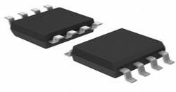
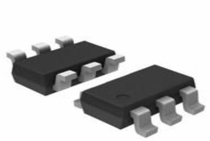
6 Terminals 2.5V 6-Pin LV62568 DC DC Voltage Regulator SWITCHING REGULATOR 1 Outputs 1.5MHz Tape & Reel (TR) SOT-563, SOT-666


6 Terminals 2.5V 6-Pin LV62568 DC DC Voltage Regulator SWITCHING REGULATOR 1 Outputs 1.5MHz Tape & Reel (TR) SOT-563, SOT-666
The TLV62568DRLT is a synchronous step-down buck DC-DC converter with a small solution size and high efficiency. The gadget includes switches that can deliver up to 1 A of output current. The following article is going to introduce the pinout, features, CAD Model, etc.
TLV62568DRLT Description
The TLV62568DRLT is a high-efficiency synchronous step-down buck DC-DC converter with a small solution size. Switches with a current output of up to 1 A are included in the device. The gadget operates in pulse width modulation (PWM) mode with a 1.5-MHz switching frequency at medium to heavy loads. The device enters Power Save Mode (PSM) at a low load to maintain high efficiency across the whole load current range. The current consumption is lowered to less than 2 A when the device is turned off.
The TLV62568DRLT uses an external resistor divider to generate a variable output voltage. During startup, an inbuilt soft-start circuit reduces the inrush current. Over-current protection, thermal shutdown protection, and power good are all built-in features. SOT23 and SOT563 packages are available for the device.
TLV62568DRLT Pinout

TLV62568DRLT CAD Model
Symbol

Footprint

3D Model

TLV62568DRLT Features
• Up to 95% Efficiency
• Low RDS(ON) Switches 150 mΩ / 100 mΩ
• 2.5-V to 5.5-V Input Voltage Range
• Adjustable Output Voltage from 0.6 V to VIN
• Power Save Mode for Light Load Efficiency
• 100% Duty Cycle for Lowest Dropout
• 35-µA Operating Quiescent Current
• 1.5-MHz Switching Frequency
• Power Good Output
• Over Current Protection
• Internal Soft Startup
• Thermal Shutdown Protection
• Available in SOT Package
• Pin-to-Pin Compatible with TLV62569
• Create a Custom Design Using the TLV62568
With the WEBENCH® Power Designer
TLV62568DRLT Functional Block Diagram

TLV62568DRLT Equivalent

TLV62568DRLT Application
• General Purpose POL Supply
• Network Video Camera
• Set Top Box
• Wireless Router

Typical Application
Specifications
- TypeParameter
- Lifecycle Status
Lifecycle Status refers to the current stage of an electronic component in its product life cycle, indicating whether it is active, obsolete, or transitioning between these states. An active status means the component is in production and available for purchase. An obsolete status indicates that the component is no longer being manufactured or supported, and manufacturers typically provide a limited time frame for support. Understanding the lifecycle status is crucial for design engineers to ensure continuity and reliability in their projects.
ACTIVE (Last Updated: 3 days ago) - Factory Lead Time6 Weeks
- Mounting Type
The "Mounting Type" in electronic components refers to the method used to attach or connect a component to a circuit board or other substrate, such as through-hole, surface-mount, or panel mount.
Surface Mount - Package / Case
refers to the protective housing that encases an electronic component, providing mechanical support, electrical connections, and thermal management.
SOT-563, SOT-666 - Surface Mount
having leads that are designed to be soldered on the side of a circuit board that the body of the component is mounted on.
YES - Number of Pins6
- Operating Temperature
The operating temperature is the range of ambient temperature within which a power supply, or any other electrical equipment, operate in. This ranges from a minimum operating temperature, to a peak or maximum operating temperature, outside which, the power supply may fail.
-40°C~125°C TJ - Packaging
Semiconductor package is a carrier / shell used to contain and cover one or more semiconductor components or integrated circuits. The material of the shell can be metal, plastic, glass or ceramic.
Tape & Reel (TR) - JESD-609 Code
The "JESD-609 Code" in electronic components refers to a standardized marking code that indicates the lead-free solder composition and finish of electronic components for compliance with environmental regulations.
e3 - Pbfree Code
The "Pbfree Code" parameter in electronic components refers to the code or marking used to indicate that the component is lead-free. Lead (Pb) is a toxic substance that has been widely used in electronic components for many years, but due to environmental concerns, there has been a shift towards lead-free alternatives. The Pbfree Code helps manufacturers and users easily identify components that do not contain lead, ensuring compliance with regulations and promoting environmentally friendly practices. It is important to pay attention to the Pbfree Code when selecting electronic components to ensure they meet the necessary requirements for lead-free applications.
yes - Part Status
Parts can have many statuses as they progress through the configuration, analysis, review, and approval stages.
Active - Moisture Sensitivity Level (MSL)
Moisture Sensitivity Level (MSL) is a standardized rating that indicates the susceptibility of electronic components, particularly semiconductors, to moisture-induced damage during storage and the soldering process, defining the allowable exposure time to ambient conditions before they require special handling or baking to prevent failures
1 (Unlimited) - Number of Terminations6
- Terminal Finish
Terminal Finish refers to the surface treatment applied to the terminals or leads of electronic components to enhance their performance and longevity. It can improve solderability, corrosion resistance, and overall reliability of the connection in electronic assemblies. Common finishes include nickel, gold, and tin, each possessing distinct properties suitable for various applications. The choice of terminal finish can significantly impact the durability and effectiveness of electronic devices.
Matte Tin (Sn) - Terminal Position
In electronic components, the term "Terminal Position" refers to the physical location of the connection points on the component where external electrical connections can be made. These connection points, known as terminals, are typically used to attach wires, leads, or other components to the main body of the electronic component. The terminal position is important for ensuring proper connectivity and functionality of the component within a circuit. It is often specified in technical datasheets or component specifications to help designers and engineers understand how to properly integrate the component into their circuit designs.
DUAL - Terminal Form
Occurring at or forming the end of a series, succession, or the like; closing; concluding.
FLAT - Peak Reflow Temperature (Cel)
Peak Reflow Temperature (Cel) is a parameter that specifies the maximum temperature at which an electronic component can be exposed during the reflow soldering process. Reflow soldering is a common method used to attach electronic components to a circuit board. The Peak Reflow Temperature is crucial because it ensures that the component is not damaged or degraded during the soldering process. Exceeding the specified Peak Reflow Temperature can lead to issues such as component failure, reduced performance, or even permanent damage to the component. It is important for manufacturers and assemblers to adhere to the recommended Peak Reflow Temperature to ensure the reliability and functionality of the electronic components.
NOT SPECIFIED - Terminal Pitch
The center distance from one pole to the next.
0.5mm - Time@Peak Reflow Temperature-Max (s)
Time@Peak Reflow Temperature-Max (s) refers to the maximum duration that an electronic component can be exposed to the peak reflow temperature during the soldering process, which is crucial for ensuring reliable solder joint formation without damaging the component.
NOT SPECIFIED - Base Part Number
The "Base Part Number" (BPN) in electronic components serves a similar purpose to the "Base Product Number." It refers to the primary identifier for a component that captures the essential characteristics shared by a group of similar components. The BPN provides a fundamental way to reference a family or series of components without specifying all the variations and specific details.
LV62568 - Function
The parameter "Function" in electronic components refers to the specific role or purpose that the component serves within an electronic circuit. It defines how the component interacts with other elements, influences the flow of electrical signals, and contributes to the overall behavior of the system. Functions can include amplification, signal processing, switching, filtering, and energy storage, among others. Understanding the function of each component is essential for designing effective and efficient electronic systems.
Step-Down - Number of Outputs1
- Output Voltage
Output voltage is a crucial parameter in electronic components that refers to the voltage level produced by the component as a result of its operation. It represents the electrical potential difference between the output terminal of the component and a reference point, typically ground. The output voltage is a key factor in determining the performance and functionality of the component, as it dictates the level of voltage that will be delivered to the connected circuit or load. It is often specified in datasheets and technical specifications to ensure compatibility and proper functioning within a given system.
5.5V - Output Type
The "Output Type" parameter in electronic components refers to the type of signal or data that is produced by the component as an output. This parameter specifies the nature of the output signal, such as analog or digital, and can also include details about the voltage levels, current levels, frequency, and other characteristics of the output signal. Understanding the output type of a component is crucial for ensuring compatibility with other components in a circuit or system, as well as for determining how the output signal can be utilized or processed further. In summary, the output type parameter provides essential information about the nature of the signal that is generated by the electronic component as its output.
Adjustable - Voltage - Input (Min)
Voltage - Input (Min) refers to the minimum voltage level that an electronic component requires to operate correctly. It indicates the lowest voltage that can be applied to the component while still allowing it to function as intended. If the input voltage falls below this specified minimum, the component may not perform properly or may fail to operate altogether. This parameter is critical for ensuring reliable operation and longevity of the device in electronic circuits.
2.5V - Input Voltage-Nom
Input Voltage-Nom refers to the nominal or rated input voltage that an electronic component or device is designed to operate within. This parameter specifies the voltage level at which the component is expected to function optimally and safely. It is important to ensure that the actual input voltage supplied to the component does not exceed this nominal value to prevent damage or malfunction. Manufacturers provide this specification to guide users in selecting the appropriate power supply or input voltage source for the component. It is a critical parameter to consider when designing or using electronic circuits to ensure reliable performance and longevity of the component.
5V - Analog IC - Other Type
Analog IC - Other Type is a parameter used to categorize electronic components that are integrated circuits (ICs) designed for analog signal processing but do not fall into more specific subcategories such as amplifiers, comparators, or voltage regulators. These ICs may include specialized analog functions such as analog-to-digital converters (ADCs), digital-to-analog converters (DACs), voltage references, or signal conditioning circuits. They are typically used in various applications where precise analog signal processing is required, such as in audio equipment, instrumentation, communication systems, and industrial control systems. Manufacturers provide detailed specifications for these components to help engineers select the most suitable IC for their specific design requirements.
SWITCHING REGULATOR - Output Configuration
Output Configuration in electronic components refers to the arrangement or setup of the output pins or terminals of a device. It defines how the output signals are structured and how they interact with external circuits or devices. The output configuration can determine the functionality and compatibility of the component in a circuit design. Common types of output configurations include single-ended, differential, open-drain, and push-pull configurations, each serving different purposes and applications in electronic systems. Understanding the output configuration of a component is crucial for proper integration and operation within a circuit.
Positive - Voltage - Output (Min/Fixed)
Voltage - Output (Min/Fixed) refers to the minimum fixed output voltage level that an electronic component, such as a voltage regulator or power supply, is designed to provide under specified load conditions. This parameter ensures that the device consistently delivers a reliable voltage that meets the requirements of the connected circuits or components. It is critical for applications where stable and predictable voltage is necessary for proper operation.
0.6V - Topology
In the context of electronic components, "topology" refers to the arrangement or configuration of the components within a circuit or system. It defines how the components are connected to each other and how signals flow between them. The choice of topology can significantly impact the performance, efficiency, and functionality of the electronic system. Common topologies include series, parallel, star, mesh, and hybrid configurations, each with its own advantages and limitations. Designers carefully select the appropriate topology based on the specific requirements of the circuit to achieve the desired performance and functionality.
Buck - Frequency - Switching
"Frequency - Switching" in electronic components refers to the rate at which a device, such as a transistor or switching regulator, turns on and off during operation. This parameter is crucial in determining the efficiency and performance of power converters, oscillators, and other circuits that rely on rapid switching. Higher switching frequencies typically allow for smaller component sizes but may require more advanced design considerations to manage heat and electromagnetic interference.
1.5MHz - Control Technique
In electronic components, "Control Technique" refers to the method or approach used to regulate and manage the operation of the component. This parameter is crucial in determining how the component functions within a circuit or system. Different control techniques can include analog control, digital control, pulse-width modulation (PWM), and various feedback mechanisms. The choice of control technique can impact the performance, efficiency, and overall functionality of the electronic component. It is important to select the appropriate control technique based on the specific requirements and characteristics of the application in which the component will be used.
PULSE WIDTH MODULATION - Synchronous Rectifier
Synchronous rectification is a technique for improving the efficiency of rectification by replacing diodes with actively controlled switches, usually power MOSFETs or power bipolar junction transistors (BJT).
Yes - Height600μm
- Length1.6mm
- Width1.2mm
- Thickness
Thickness in electronic components refers to the measurement of how thick a particular material or layer is within the component structure. It can pertain to various aspects, such as the thickness of a substrate, a dielectric layer, or conductive traces. This parameter is crucial as it impacts the electrical, mechanical, and thermal properties of the component, influencing its performance and reliability in electronic circuits.
550μm - RoHS Status
RoHS means “Restriction of Certain Hazardous Substances” in the “Hazardous Substances Directive” in electrical and electronic equipment.
ROHS3 Compliant
TLV62568DRLT Package


TLV62568DRLT Manufacturer
Texas Instruments Incorporated (TI) is an American technology company based in Dallas, Texas, that designs and manufactures semiconductors and various integrated circuits, which it sells to electronics designers and manufacturers globally. It is one of the top 10 semiconductor companies worldwide based on sales volume. The company's focus is on developing analog chips and embedded processors, which account for more than 80% of its revenue. TI also produces TI digital light processing technology and education technology products including calculators, microcontrollers, and multi-core processors. The company boasts 45,000 patents around the globe as of 2016.
Trend Analysis
Parts with Similar Specs
Datasheet PDF
- Datasheets :
- PCN Assembly/Origin :
What is TLV62568DRLT?
The TLV62568DRLT is a high-efficiency synchronous step-down buck DC-DC converter with a small solution size. Switches with a current output of up to 1 A are included in the device.The gadget operates in pulse width modulation (PWM) mode with a 1.5-MHz switching frequency at medium to heavy loads. The device enters Power Save Mode (PSM) at low load to maintain high efficiency across the whole load current range. The current consumption is lowered to less than 2 A when the device is turned off.
What is the output current of the TLV62568DRLT?
1A.
 THS4631 Op-Amp : Price, Alternatives, Datasheet
26 July 20212444
 A Comprehensive Guide to LTC6603CUF#TRPBF Active Filter
06 March 2024107
 DS1820 Digital Thermometer: Pinout, Datasheet and Comparison
04 August 20215714
 A Comprehensive Guide to LTC6953IUKG#TRPBF Clock Generator by Linear Technology/Analog Devices
06 March 2024244
 BU406 Transistor: Equivalent, Datasheet and Pinout
15 November 202115216
 BME680 Temperature & Humidity & Gas Sensor: BME280 vs BME680, Datasheet, Pinout
20 January 20228012
 DAC081S101CIMKXNOPB:DAC, Piniout, Full-Featured
16 February 2022247
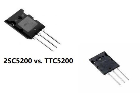 2SC5200 vs.TTC5200
08 July 202212976
 Wiring and Mounting Photoelectric Sensors in 2025
15 July 2025916
 What is a Biosensor?
23 March 20213340
 What is a DC-to-DC Converter?
23 April 20216781
 How are Integrated Circuits produced?
20 October 202525267
 Revolutionizing the Electric Vehicle Industry with Silicon Carbide
10 August 20231865
 Introduction to Microprocessors
18 August 202018131
 Tech Giants Accelerate In-House Semiconductor Design, Threatening Fabless Chipmakers
27 September 20233014
 What is Chip: Definition, Classification and Design Process
17 January 20265564
Texas Instruments
In Stock: 1800
United States
China
Canada
Japan
Russia
Germany
United Kingdom
Singapore
Italy
Hong Kong(China)
Taiwan(China)
France
Korea
Mexico
Netherlands
Malaysia
Austria
Spain
Switzerland
Poland
Thailand
Vietnam
India
United Arab Emirates
Afghanistan
Åland Islands
Albania
Algeria
American Samoa
Andorra
Angola
Anguilla
Antigua & Barbuda
Argentina
Armenia
Aruba
Australia
Azerbaijan
Bahamas
Bahrain
Bangladesh
Barbados
Belarus
Belgium
Belize
Benin
Bermuda
Bhutan
Bolivia
Bonaire, Sint Eustatius and Saba
Bosnia & Herzegovina
Botswana
Brazil
British Indian Ocean Territory
British Virgin Islands
Brunei
Bulgaria
Burkina Faso
Burundi
Cabo Verde
Cambodia
Cameroon
Cayman Islands
Central African Republic
Chad
Chile
Christmas Island
Cocos (Keeling) Islands
Colombia
Comoros
Congo
Congo (DRC)
Cook Islands
Costa Rica
Côte d’Ivoire
Croatia
Cuba
Curaçao
Cyprus
Czechia
Denmark
Djibouti
Dominica
Dominican Republic
Ecuador
Egypt
El Salvador
Equatorial Guinea
Eritrea
Estonia
Eswatini
Ethiopia
Falkland Islands
Faroe Islands
Fiji
Finland
French Guiana
French Polynesia
Gabon
Gambia
Georgia
Ghana
Gibraltar
Greece
Greenland
Grenada
Guadeloupe
Guam
Guatemala
Guernsey
Guinea
Guinea-Bissau
Guyana
Haiti
Honduras
Hungary
Iceland
Indonesia
Iran
Iraq
Ireland
Isle of Man
Israel
Jamaica
Jersey
Jordan
Kazakhstan
Kenya
Kiribati
Kosovo
Kuwait
Kyrgyzstan
Laos
Latvia
Lebanon
Lesotho
Liberia
Libya
Liechtenstein
Lithuania
Luxembourg
Macao(China)
Madagascar
Malawi
Maldives
Mali
Malta
Marshall Islands
Martinique
Mauritania
Mauritius
Mayotte
Micronesia
Moldova
Monaco
Mongolia
Montenegro
Montserrat
Morocco
Mozambique
Myanmar
Namibia
Nauru
Nepal
New Caledonia
New Zealand
Nicaragua
Niger
Nigeria
Niue
Norfolk Island
North Korea
North Macedonia
Northern Mariana Islands
Norway
Oman
Pakistan
Palau
Palestinian Authority
Panama
Papua New Guinea
Paraguay
Peru
Philippines
Pitcairn Islands
Portugal
Puerto Rico
Qatar
Réunion
Romania
Rwanda
Samoa
San Marino
São Tomé & Príncipe
Saudi Arabia
Senegal
Serbia
Seychelles
Sierra Leone
Sint Maarten
Slovakia
Slovenia
Solomon Islands
Somalia
South Africa
South Sudan
Sri Lanka
St Helena, Ascension, Tristan da Cunha
St. Barthélemy
St. Kitts & Nevis
St. Lucia
St. Martin
St. Pierre & Miquelon
St. Vincent & Grenadines
Sudan
Suriname
Svalbard & Jan Mayen
Sweden
Syria
Tajikistan
Tanzania
Timor-Leste
Togo
Tokelau
Tonga
Trinidad & Tobago
Tunisia
Turkey
Turkmenistan
Turks & Caicos Islands
Tuvalu
U.S. Outlying Islands
U.S. Virgin Islands
Uganda
Ukraine
Uruguay
Uzbekistan
Vanuatu
Vatican City
Venezuela
Wallis & Futuna
Yemen
Zambia
Zimbabwe
![LM2574HVMX-3.3]() LM2574HVMX-3.3
LM2574HVMX-3.3Texas Instruments
![LM25574MTX]() LM25574MTX
LM25574MTXTexas Instruments
![LM2577MX-ADJ]() LM2577MX-ADJ
LM2577MX-ADJTexas Instruments
![TLV62565DBVR]() TLV62565DBVR
TLV62565DBVRTexas Instruments
![LM25011MY/NOPB]() LM25011MY/NOPB
LM25011MY/NOPBTexas Instruments
![LM2575T-5.0/NOPB]() LM2575T-5.0/NOPB
LM2575T-5.0/NOPBTexas Instruments
![MC33063ADR]() MC33063ADR
MC33063ADRTexas Instruments
![LM2675MX-ADJ/NOPB]() LM2675MX-ADJ/NOPB
LM2675MX-ADJ/NOPBTexas Instruments
![LM2574N-5.0/NOPB]() LM2574N-5.0/NOPB
LM2574N-5.0/NOPBTexas Instruments
![LM2576SX-5.0/NOPB]() LM2576SX-5.0/NOPB
LM2576SX-5.0/NOPBTexas Instruments


