Product
 Brand
Brand Articles
 Tools
Tools
Designing a GaN-based Dual Active Bridge for PHEV Chargers
When it comes to previous research and applications, using high voltage normally-off Gallium Nitride (GaN) devices, has paved the way for high power density and efficiency in bidirectional battery chargers. However, the topology for such chargers demands careful consideration. While widely adopted topologies like LLC resonant converters and phase shift full bridge converters have several advantages, they fall short in the context of bidirectional chargers employing GaN devices. There was hence the requirement for an optimized, high-frequency-efficiency dual active bridge converter (DAB) for battery charging applications.
GaN Multi-chip Module and its Characterization
To meet high current requirements, multiple GaN devices connected in parallel, with 6 to 8 devices typically paralleled were used as a test circuit. As shown in Figure 1, a half-bridge configuration served as the core topology, aided by ceramic capacitors for decoupling, significantly reducing loop inductance to 3.6 nH. This layout ensured an even distribution of power loops which was crucial for the optimal performance of the system.

Figure 1: Bidirectional battery charger topology using GaN
Figure 2 shows how on-resistance varies with junction temperature, while the absence of a body diode in normally-off GaN devices leads to a significant reverse conduction voltage drop. Dynamic Ron is seen as initial instability post-activation, stabilizing over time, and how the output capacitance measurements are essential for predicting zero-voltage switching (ZVS) transition times. Despite challenges posed by limited datasheet insights, direct characterization methods offered reliable solutions during this test. The integration of parallel-connected GaN devices, accurate layout design, and precise gate signal management ensured optimal performance in high-current applications. By ensuring thorough semiconductor characterization, engineers can gain valuable insights into device behavior, enabling informed decision-making for system optimization.

Figure 2: Voltage drop observed when reverse conduction takes place at a different current
Optimizing Parameters for DAB and its Selection for Efficiency
Initially, a DAB converter was designed to operate at 250V input and output, delivering 1kW power at 500 kHz. In order to match the energy transfer needs, an inductance model was used, resulting in a 2.7 µH inductor due to practical constraints, along with transformer leakage, creating a total commutation inductance of 3.36 µH. In this setup, there was an efficiency of 97.2% achieved wherein the loss breakdown revealed GaN device and transformer/inductor losses each accounted for 42%, with additional losses from PCB traces and Litz wire termination. Moreover, it was also noted that GaN device losses increase during hard-switching. Figure 3 illustrates the loss breakdown.

Figure 3: Maximum output current of the DAB
Optimizing the performance of a Plug-in Hybrid Electric Vehicle (PHEV) battery charger takes into consideration several critical parameters like the transformer turns ratio and commutation inductance (Llk). The efficiency of the converter varies with load conditions, particularly concerning the charger's ability to accommodate voltage fluctuations ranging from 270V to 430V. To ensure optimal efficiency within the battery voltage range of 310V to 390V, where the charger delivers a steady 3.3kW output, precise design choices are crucial for its operation. Selecting a DC link voltage of 350V simplifies the determination of a 1:1 transformer turns ratio. This decision aligns the charger's highest efficiency point with the mid-range battery voltage of 350V, enhancing overall performance. Moreover, adopting a sinusoidal charging methodology minimizes the reliance on DC link capacitance. In this approach, the output current regulation is achieved through a precise control of phase shift (φ) across the line cycle.

Figure 4: Conduction losses at 310V, 350V and 390V with the commutation inductance value up to 4 µH
This Sinusoidal charging could confirm that the peak output current was double the average, necessitating a commutation inductance lower than 4 µH to facilitate full 3.3kW power delivery at 310V. Phase shift modulation enabled a soft-switching turn-on for all eight switches within the charger architecture and the Zero Voltage Switching (ZVS) boundary, influenced by GaN device output capacitance, played a pivotal role in determining optimal operation conditions. Moreover, further analysis revealed that switching loss decreases with higher inductance, owing to the extended ZVS range. Notably, the lowest loss occurs at a battery voltage of 350V, attributed to the widest ZVS range at this voltage level. Conduction loss follows a similar trend, with the lowest observed again at 350V battery voltage. Despite this, selecting the optimal commutation inductance to minimize the total losses presents a nuanced challenge, necessitating consideration of total energy loss over the charging duration. Figure 4 illustrates the total semiconductor loss trends for different battery voltages, aiding in the comprehensive analysis of charger performance.
Conclusion
An experiment was conducted to optimize a Dual Active Bridge (DAB) converter for Plug-in Hybrid Electric Vehicle (PHEV) chargers, considering the challenges of a wide battery voltage range and fluctuating output current. By characterizing GaN multi-chip modules, the commutation inductance was determined for minimal energy loss throughout the charging cycle. Integration of this inductance value into a high-frequency transformer enabled the DAB converter to achieve 97.2% efficiency at 1 kW, operating at 500 kHz.
 UTMEL
UTMEL
We are the professional distributor of electronic components, providing a large variety of products to save you a lot of time, effort, and cost with our efficient self-customized service. careful order preparation fast delivery service
 Improving the Energy Conversion Efficiency of Triboelectric NanogeneratorsSaumitra Jagdale19 November 20243225
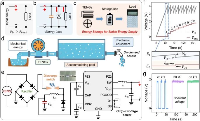
There is a huge growth in demand for self-sustaining electronic devices, as the traditional power-generating devices fail in remote and harsh environments due to the periodic requirement of battery changes. Also, these devices are frequency specific; some work only in high frequency and some in low frequency. Triboelectric nanogenerators (TENGs) provide a promising solution by efficiently converting mechanical energy into electricity as they are versatile, compact, and cheap, making them a popular choice.
Read More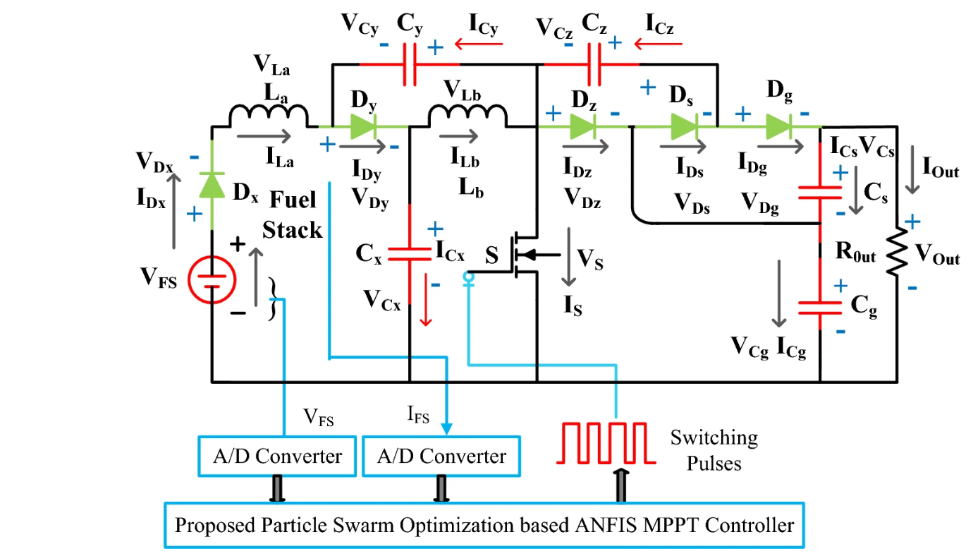 Methodologies for Increasing Efficiency of Fuel Stack Technology for Energy GenerationSaumitra Jagdale19 November 20243081
Presently, power companies are moving towards renewable energy systems. Conventional energy sources are more expensive because they require a vast network to be maintained and huge human resources. Also, they harm the environment by releasing several harmful gases. As the industry’s focus shifts toward renewable energy sources, energy systems powered by Proton Exchange Membrane Fuel Stacks (PEMFS) are gaining traction.
Read More VSC Light Meaning, Causes, and Step-by-Step DiagnosticsUTMEL19 May 20262923
A VSC (Vehicle Stability Control) light indicates the system is disabled, often as a fail-safe triggered by unrelated engine faults like a loose gas cap. While the stability system prevents lateral skidding, it shuts down when sensor data is unreliable. Proper diagnosis requires an ABS-capable OBD2 scanner. Resolving the root engine code, checking wheel speed sensors, or performing a zero-point calibration usually restores system function.
Read More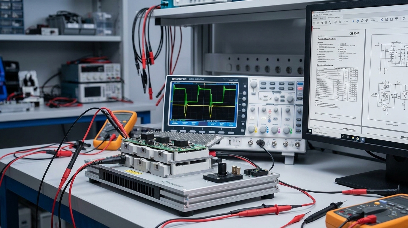 What JEDEC JEP203 and JEP204 Actually Change for SiC Qualification Engineers and Component BuyersUTMEL29 July 2026417
Summary: When JEDEC published JEP203 and JEP204 on June 3, 2026[1], most coverage treated them as an announcement. They are better understood as the first shared language the silicon carbide industry has had for two problems that have quietly consumed engineering hours since the first commercial SiC MOSFETs shipped: short-circuit evaluation that produces numbers you can compare across suppliers, and a consolidated reference of stress procedures so qualification engineers stop reinventing test plans from scratch. This article explains what changes on Monday morning and what to ask suppliers for now.
Read More 2nm vs 3nm Chips: What the Latest Process Nodes Mean for PerformanceUTMEL19 August 20261217
The shift from 3nm to 2nm process nodes marks a fundamental change in transistor architecture, moving from FinFET to Gate-All-Around (GAA) nanosheets. This transition delivers meaningful improvements in performance, power, and density, but also introduces new challenges like SRAM scaling limits, thermal density, and backside power delivery. The article compares TSMC, Samsung, and Intel approaches, offering a practical decision framework for engineering teams.
Read More
Subscribe to Utmel !
![200217-1400]() 200217-1400
200217-1400Molex
![63808-4310]() 63808-4310
63808-4310Molex
![63808-2300]() 63808-2300
63808-2300Molex
![63808-4300]() 63808-4300
63808-4300Molex
![63904-6500]() 63904-6500
63904-6500Molex
![63808-2710]() 63808-2710
63808-2710Molex
![63808-2610]() 63808-2610
63808-2610Molex
![63808-3400]() 63808-3400
63808-3400Molex
![63808-2410]() 63808-2410
63808-2410Molex
![203702-1900]() 203702-1900
203702-1900Molex