Kyoto University Successfully Demonstrates That SiC Can Also Work at 350°C

Silicon Carbide - The subtle REVOLUTION
Kyoto University (KU) recently announced that it has successfully demonstrated basic operation at high temperatures of 350°C, where Si semiconductor integrated circuits cannot operate, using SiC semiconductor integrated circuits.
The result is based on the research team of Assistant Professor Bright Kaneko and Professor Tsunobu Kimoto at the Graduate School of Engineering, Kyoto University. Details were presented on March 25 at the "69th Japan Society of Applied Physics Spring Lecture Meeting" held online from March 22 to 26 at Aoyama Gakuin University Sagamihara Campus.
It is said that Si semiconductors fail at about 250°C and cannot operate in higher temperatures. Therefore, it is expected to use SiC integrated circuits that have better heat resistance and can operate even at about 800°C. However, if structures similar to transistors in Si integrated circuits are fabricated from SiC, the characteristics will be difficult to control reliability in high-temperature environments due to SiC-specific defects, and there are problems of high power consumption.
To solve these problems, transistors for SiC integrated circuits with structures different from MOSFETs in Si integrated circuits are being developed, in which JFETs do not have physical interface defects in the current flow region as MOSFETs do. Therefore, it is promising as a transistor that constitutes a SiC integrated circuit with high-temperature action.
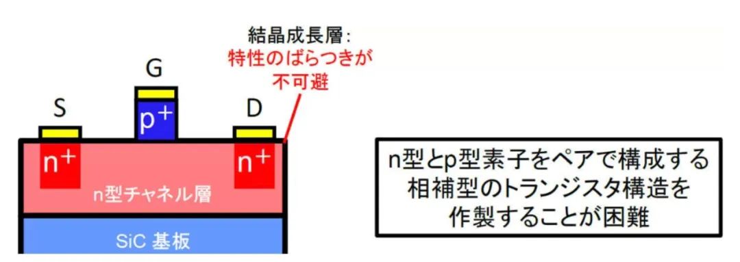
However, JFETs fabricated by the general method require large standby power and low power consumption because they cannot form a complementary circuit with a combination of n-type and p-type on the same substrate as MOSFETs, and conversion is required.

Schematic diagram of an n-type JFET fabricated by the general method (crystal growth)
(Source: Kyoto University Press Release PDF)
In this context, the research team has proposed a unique transistor structure and circuit configuration. It is said to have successfully demonstrated the operation of SiC logic gates from room temperature to 350°C with low power consumption.
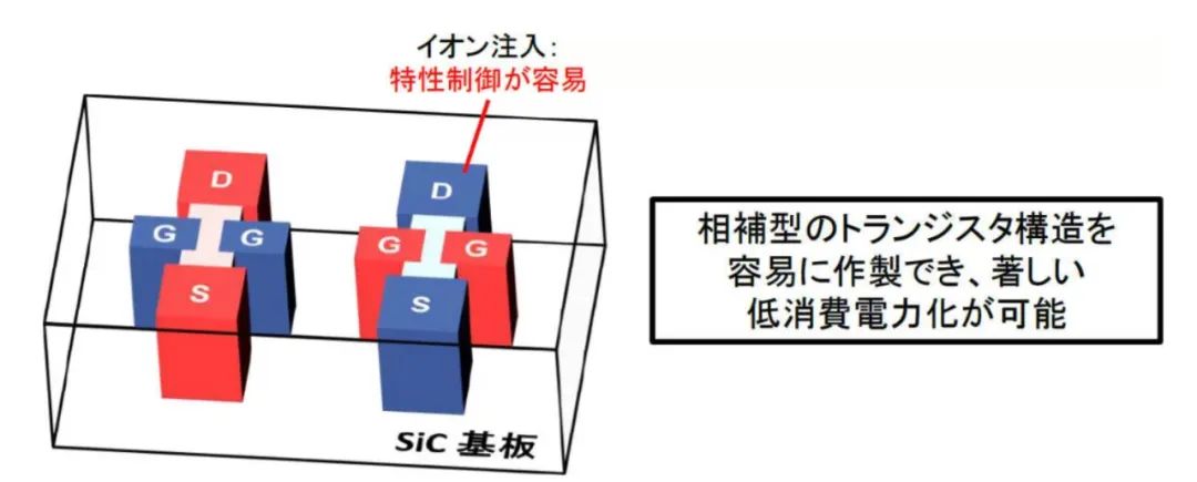
There are two points of implementation. The first is the realization of a technique to fabricate both n-type and p-type on the same substrate, which is not possible with conventional general-purpose JFET fabrication methods. It is said to have succeeded in producing both n-type and p-type JFETs on the same substrate by performing ion implantation for local conductivity type control of the entire device structure.

Schematic diagram of n-type and p-type JFETs produced by the proposed method (ion implantation) (Source: Kyoto University Press Release PDF)
The second is that the JFET achieves a normally-off type characteristic, i.e., a characteristic that does not allow current to flow as a transistor when no voltage is applied to the gate terminal. This characteristic is also said to be difficult to achieve by the general JFET fabrication method, but by using a dual-gate structure, which constitutes the gate region by clamping the channel region from both sides, a normally off-type JFET can be fabricated. is said to have been accomplished.
It has been confirmed that the fabricated complementary JFETs operate normally in the temperature range from room temperature to 350°C, and that the power consumption in the standby state can be suppressed to a maximum of a few tens of nW or less.
The research team explained that the advantage of this research is that the circuit presented here can be fabricated using standard processes for SiC semiconductors as power semiconductors, but we will continue with MOSFETs, and further fundamental research is needed to determine if JFETs can be made smaller, faster, and more precise by miniaturization, and continued research is needed.
Related News
1、MediaTek, Qualcomm announce joining Russia sanctions
2、Automotive chips rose across the board!
3、Apple M1 Ultra -- The Technology Behind the Chip Interconnection
4、Foxconn Announces Investment of $9 Billion to Build A Chip Factory in Saudi Arabia
5、Japanese Companies Increase Investment in Power Semiconductors
 UTMEL 2024 Annual gala: Igniting Passion, Renewing BrillianceUTMEL18 January 20244823
As the year comes to an end and the warm sun rises, Utmel Electronics celebrates its 6th anniversary.
Read More Electronic Components Distributor Utmel to Showcase at 2024 IPC APEX EXPOUTMEL10 April 20245810
Utmel, a leading electronic components distributor, is set to make its appearance at the 2024 IPC APEX EXPO.
Read More Electronic components distributor UTMEL to Showcase at electronica ChinaUTMEL07 June 20244398
The three-day 2024 Electronica China will be held at the Shanghai New International Expo Center from July 8th to 10th, 2024.
Read More Electronic components distributor UTMEL Stands Out at electronica china 2024UTMEL09 July 20244761
From July 8th to 10th, the three-day electronica china 2024 kicked off grandly at the Shanghai New International Expo Center.
Read More A Combo for Innovation: Open Source and CrowdfundingUTMEL15 November 20195349
Open source is already known as a force multiplier, a factor that makes a company's staff, financing, and resources more effective. However, in the last few years, open source has started pairing with another force multiplier—crowdfunding. Now the results of this combination are starting to emerge: the creation of small, innovative companies run by design engineers turned entrepreneurs. Although the results are just starting to appear, they include a fresh burst of product innovation and further expansion of open source into business.
Read More
Subscribe to Utmel !
![PT15NV18-04631]() PT15NV18-04631
PT15NV18-04631Amphenol
![PT15LV18-10305]() PT15LV18-10305
PT15LV18-10305Amphenol
![PT6KH-02282]() PT6KH-02282
PT6KH-02282Amphenol
![PT15NH06-08515]() PT15NH06-08515
PT15NH06-08515Amphenol
![PT15WH06-04352]() PT15WH06-04352
PT15WH06-04352Amphenol
![PTC10LH01-00545]() PTC10LH01-00545
PTC10LH01-00545Amphenol
![PT15LV18-07074]() PT15LV18-07074
PT15LV18-07074Amphenol
![PTC10LV10-00645]() PTC10LV10-00645
PTC10LV10-00645Amphenol
![PT15NV18-01141]() PT15NV18-01141
PT15NV18-01141Amphenol
![PS10MV50-42240]() PS10MV50-42240
PS10MV50-42240Amphenol


 Product
 Brand
Brand Articles
 Tools
Tools


