
 Product
 Brand
Brand Articles
 Tools
Tools
2N3773 Transistor: 2N3773, Circuit Diagram, Equivalent


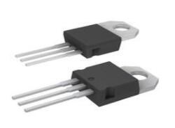
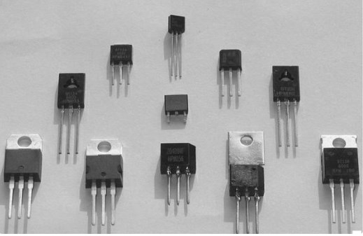
TRANS NPN 140V 16A TO-3
The 2N3773 is a planar NPN transistor mounted in a TO-3 metal case. This article will unlock more details about 2N3773. There is a huge range of Semiconductors, Capacitors, Resistors and ICs in stock. Welcome RFQ.

2n3773 300 watt NPN amplifier circuit diagram
2N3773 Pinout

2N3773 Pinout
2N3773 CAD Model
Symbol

2N3773 Symbol
Footprint

2N3773 Footprint
2N3773 Description
The 2n3773 is a bipolar transistor with an NPN power base that is primarily used in disk head positioners, high-power audio, and other linear applications.
Because of its strong switching capability, this power transistor is also used in power-switching circuits like relays, DC-DC converters, and solenoid drivers.
The emitter, base, and collector terminals make up the majority of the 2n3773.
It has a high DC current gain and a low saturation voltage, and it is properly described for linear operation.
2N3773 Feature
• High Safe Operating Area (100% Tested) 150 W @ 100 V
• Completely Characterized for Linear Operation
• High DC Current Gain and Low Saturation Voltage hFE = 15 (Min) @ 8.0 A, 4.0 V VCE(sat) = 1.4 V (Max) @ IC = 8.0 A, IB = 0.8 A
• For Low Distortion Complementary Designs
• This is a Pb−Free Device
2N3773 Application
High power audio and Linear Applications
High-performance switching and amplification purpose
2N3773 Equivalent
The equivalent for 2N3773:
2N3000
2N3009
2N3010
2N3011
2N3012
2N3013
2N3773 Circuit Diagram
This NPN transistor is a bipolar current-controlled device, as opposed to a unipolar voltage-controlled device like a JFET.
The collector voltage exceeds the base voltage, which is positive in relation to the emitter.
The total of the base and collector currents is the emitter current.
This NPN transistor can be used with three configurations i.e common emitter configuration, common base configuration, and common collector configuration.
Because it has the requisite voltage and power gain for the amplification process, the common-emitter arrangement is primarily employed for amplification. The circuit diagram for 2N3773 is shown below.

2N3773 Circuit Diagram
The size and doping concentration of the collector and emitter terminals varies. The emitter has a high doping level, while the collector has a low doping level.
The forward current gain of a transistor is an essential aspect in determining its features. It's an amplification factor, which means it's a measure of how much current is amplified. It's called Beta, and it's a ratio between collector current and base current that's denoted by. The beta value ranges from 20 to 1000, with 200 being the most common. It has no unit because it is a ratio of two currents.
Another key aspect is current gain, which is indicated by and represents a ratio between collector and emitter current. The alpha value varies from 0.95 to 0.99. The majority of the time, its values are regarded as one.
Specifications
- TypeParameter
- Mount
In electronic components, the term "Mount" typically refers to the method or process of physically attaching or fixing a component onto a circuit board or other electronic device. This can involve soldering, adhesive bonding, or other techniques to secure the component in place. The mounting process is crucial for ensuring proper electrical connections and mechanical stability within the electronic system. Different components may have specific mounting requirements based on their size, shape, and function, and manufacturers provide guidelines for proper mounting procedures to ensure optimal performance and reliability of the electronic device.
Chassis Mount, Through Hole - Mounting Type
The "Mounting Type" in electronic components refers to the method used to attach or connect a component to a circuit board or other substrate, such as through-hole, surface-mount, or panel mount.
Chassis Mount - Package / Case
refers to the protective housing that encases an electronic component, providing mechanical support, electrical connections, and thermal management.
TO-204AA, TO-3 - Number of Pins2
- Transistor Element Material
The "Transistor Element Material" parameter in electronic components refers to the material used to construct the transistor within the component. Transistors are semiconductor devices that amplify or switch electronic signals and are a fundamental building block in electronic circuits. The material used for the transistor element can significantly impact the performance and characteristics of the component. Common materials used for transistor elements include silicon, germanium, and gallium arsenide, each with its own unique properties and suitability for different applications. The choice of transistor element material is crucial in designing electronic components to meet specific performance requirements such as speed, power efficiency, and temperature tolerance.
SILICON - Collector-Emitter Breakdown Voltage140V
- Collector-Emitter Saturation Voltage4V
- Number of Elements1
- hFEMin5
- Operating Temperature
The operating temperature is the range of ambient temperature within which a power supply, or any other electrical equipment, operate in. This ranges from a minimum operating temperature, to a peak or maximum operating temperature, outside which, the power supply may fail.
200°C TJ - Packaging
Semiconductor package is a carrier / shell used to contain and cover one or more semiconductor components or integrated circuits. The material of the shell can be metal, plastic, glass or ceramic.
Bulk - JESD-609 Code
The "JESD-609 Code" in electronic components refers to a standardized marking code that indicates the lead-free solder composition and finish of electronic components for compliance with environmental regulations.
e3 - Pbfree Code
The "Pbfree Code" parameter in electronic components refers to the code or marking used to indicate that the component is lead-free. Lead (Pb) is a toxic substance that has been widely used in electronic components for many years, but due to environmental concerns, there has been a shift towards lead-free alternatives. The Pbfree Code helps manufacturers and users easily identify components that do not contain lead, ensuring compliance with regulations and promoting environmentally friendly practices. It is important to pay attention to the Pbfree Code when selecting electronic components to ensure they meet the necessary requirements for lead-free applications.
yes - Part Status
Parts can have many statuses as they progress through the configuration, analysis, review, and approval stages.
Obsolete - Moisture Sensitivity Level (MSL)
Moisture Sensitivity Level (MSL) is a standardized rating that indicates the susceptibility of electronic components, particularly semiconductors, to moisture-induced damage during storage and the soldering process, defining the allowable exposure time to ambient conditions before they require special handling or baking to prevent failures
1 (Unlimited) - Number of Terminations2
- ECCN Code
An ECCN (Export Control Classification Number) is an alphanumeric code used by the U.S. Bureau of Industry and Security to identify and categorize electronic components and other dual-use items that may require an export license based on their technical characteristics and potential for military use.
EAR99 - Terminal Finish
Terminal Finish refers to the surface treatment applied to the terminals or leads of electronic components to enhance their performance and longevity. It can improve solderability, corrosion resistance, and overall reliability of the connection in electronic assemblies. Common finishes include nickel, gold, and tin, each possessing distinct properties suitable for various applications. The choice of terminal finish can significantly impact the durability and effectiveness of electronic devices.
Tin (Sn) - Max Power Dissipation
The maximum power that the MOSFET can dissipate continuously under the specified thermal conditions.
150W - Terminal Position
In electronic components, the term "Terminal Position" refers to the physical location of the connection points on the component where external electrical connections can be made. These connection points, known as terminals, are typically used to attach wires, leads, or other components to the main body of the electronic component. The terminal position is important for ensuring proper connectivity and functionality of the component within a circuit. It is often specified in technical datasheets or component specifications to help designers and engineers understand how to properly integrate the component into their circuit designs.
BOTTOM - Terminal Form
Occurring at or forming the end of a series, succession, or the like; closing; concluding.
PIN/PEG - Base Part Number
The "Base Part Number" (BPN) in electronic components serves a similar purpose to the "Base Product Number." It refers to the primary identifier for a component that captures the essential characteristics shared by a group of similar components. The BPN provides a fundamental way to reference a family or series of components without specifying all the variations and specific details.
2N37 - Pin Count
a count of all of the component leads (or pins)
2 - Element Configuration
The distribution of electrons of an atom or molecule (or other physical structure) in atomic or molecular orbitals.
Single - Power Dissipation
the process by which an electronic or electrical device produces heat (energy loss or waste) as an undesirable derivative of its primary action.
150W - Case Connection
Case Connection refers to the method by which an electronic component's case or housing is connected to the electrical circuit. This connection is important for grounding purposes, mechanical stability, and heat dissipation. The case connection can vary depending on the type of component and its intended application. It is crucial to ensure a secure and reliable case connection to maintain the overall performance and safety of the electronic device.
COLLECTOR - Transistor Application
In the context of electronic components, the parameter "Transistor Application" refers to the specific purpose or function for which a transistor is designed and used. Transistors are semiconductor devices that can amplify or switch electronic signals and are commonly used in various electronic circuits. The application of a transistor can vary widely depending on its design and characteristics, such as whether it is intended for audio amplification, digital logic, power control, or radio frequency applications. Understanding the transistor application is important for selecting the right type of transistor for a particular circuit or system to ensure optimal performance and functionality.
SWITCHING - Polarity/Channel Type
In electronic components, the parameter "Polarity/Channel Type" refers to the characteristic that determines the direction of current flow or the type of signal that can be accommodated by the component. For components like diodes and transistors, polarity indicates the direction in which current can flow through the component, such as forward bias or reverse bias for diodes. For components like MOSFETs or JFETs, the channel type refers to whether the component is an N-channel or P-channel device, which determines the type of charge carriers that carry current through the component. Understanding the polarity or channel type of a component is crucial for proper circuit design and ensuring that the component is connected correctly to achieve the desired functionality.
NPN - Transistor Type
Transistor type refers to the classification of transistors based on their operation and construction. The two primary types are bipolar junction transistors (BJTs) and field-effect transistors (FETs). BJTs use current to control the flow of current, while FETs utilize voltage to control current flow. Each type has its own subtypes, such as NPN and PNP for BJTs, and MOSFETs and JFETs for FETs, impacting their applications and characteristics in electronic circuits.
NPN - Collector Emitter Voltage (VCEO)
Collector-Emitter Voltage (VCEO) is a key parameter in electronic components, particularly in transistors. It refers to the maximum voltage that can be applied between the collector and emitter terminals of a transistor while the base terminal is open or not conducting. Exceeding this voltage limit can lead to breakdown and potential damage to the transistor. VCEO is crucial for ensuring the safe and reliable operation of the transistor within its specified limits. Designers must carefully consider VCEO when selecting transistors for a circuit to prevent overvoltage conditions that could compromise the performance and longevity of the component.
140V - Max Collector Current
Max Collector Current is a parameter used to specify the maximum amount of current that can safely flow through the collector terminal of a transistor or other electronic component without causing damage. It is typically expressed in units of amperes (A) and is an important consideration when designing circuits to ensure that the component operates within its safe operating limits. Exceeding the specified max collector current can lead to overheating, degradation of performance, or even permanent damage to the component. Designers must carefully consider this parameter when selecting components and designing circuits to ensure reliable and safe operation.
16A - DC Current Gain (hFE) (Min) @ Ic, Vce
The parameter "DC Current Gain (hFE) (Min) @ Ic, Vce" in electronic components refers to the minimum value of the DC current gain, denoted as hFE, under specific operating conditions of collector current (Ic) and collector-emitter voltage (Vce). The DC current gain hFE represents the ratio of the collector current to the base current in a bipolar junction transistor (BJT), indicating the amplification capability of the transistor. The minimum hFE value at a given Ic and Vce helps determine the transistor's performance and efficiency in amplifying signals within a circuit. Designers use this parameter to ensure proper transistor selection and performance in various electronic applications.
15 @ 8A 4V - Current - Collector Cutoff (Max)
The parameter "Current - Collector Cutoff (Max)" refers to the maximum current at which a transistor or other electronic component will cease to conduct current between the collector and emitter terminals. This parameter is important in determining the maximum current that can flow through the component when it is in the cutoff state. Exceeding this maximum cutoff current can lead to malfunction or damage of the component. It is typically specified in the component's datasheet and is crucial for proper circuit design and operation.
10mA - Vce Saturation (Max) @ Ib, Ic
The parameter "Vce Saturation (Max) @ Ib, Ic" in electronic components refers to the maximum voltage drop across the collector-emitter junction when the transistor is in saturation mode. This parameter is specified at a certain base current (Ib) and collector current (Ic) levels. It indicates the minimum voltage required to keep the transistor fully conducting in saturation mode, ensuring that the transistor operates efficiently and does not enter the cutoff region. Designers use this parameter to ensure proper transistor operation and to prevent overheating or damage to the component.
4V @ 3.2A, 16A - Collector Base Voltage (VCBO)
Collector Base Voltage (VCBO) is the maximum allowable voltage that can be applied between the collector and base terminals of a bipolar junction transistor when the emitter is open. It is a critical parameter that determines the voltage rating of the transistor and helps prevent breakdown in the collector-base junction. Exceeding this voltage can lead to permanent damage or failure of the component.
160V - Emitter Base Voltage (VEBO)
Emitter Base Voltage (VEBO) is a parameter used in electronic components, particularly in transistors. It refers to the maximum voltage that can be applied between the emitter and base terminals of a transistor without causing damage to the device. Exceeding this voltage limit can lead to breakdown of the transistor and potential failure. VEBO is an important specification to consider when designing circuits to ensure the proper operation and reliability of the components. It is typically provided in the datasheet of the transistor and should be carefully observed to prevent any potential damage during operation.
7V - Height26mm
- Length39.3mm
- Width8.92mm
- REACH SVHC
The parameter "REACH SVHC" in electronic components refers to the compliance with the Registration, Evaluation, Authorization, and Restriction of Chemicals (REACH) regulation regarding Substances of Very High Concern (SVHC). SVHCs are substances that may have serious effects on human health or the environment, and their use is regulated under REACH to ensure their safe handling and minimize their impact.Manufacturers of electronic components need to declare if their products contain any SVHCs above a certain threshold concentration and provide information on the safe use of these substances. This information allows customers to make informed decisions about the potential risks associated with using the components and take appropriate measures to mitigate any hazards.Ensuring compliance with REACH SVHC requirements is essential for electronics manufacturers to meet regulatory standards, protect human health and the environment, and maintain transparency in their supply chain. It also demonstrates a commitment to sustainability and responsible manufacturing practices in the electronics industry.
No SVHC - Radiation Hardening
Radiation hardening is the process of making electronic components and circuits resistant to damage or malfunction caused by high levels of ionizing radiation, especially for environments in outer space (especially beyond the low Earth orbit), around nuclear reactors and particle accelerators, or during nuclear accidents or nuclear warfare.
No - RoHS Status
RoHS means “Restriction of Certain Hazardous Substances” in the “Hazardous Substances Directive” in electrical and electronic equipment.
ROHS3 Compliant - Lead Free
Lead Free is a term used to describe electronic components that do not contain lead as part of their composition. Lead is a toxic material that can have harmful effects on human health and the environment, so the electronics industry has been moving towards lead-free components to reduce these risks. Lead-free components are typically made using alternative materials such as silver, copper, and tin. Manufacturers must comply with regulations such as the Restriction of Hazardous Substances (RoHS) directive to ensure that their products are lead-free and environmentally friendly.
Lead Free
Parts with Similar Specs
- ImagePart NumberManufacturerMountPackage / CaseCollector Emitter Breakdown VoltageMax Collector CurrentCollector Emitter Saturation VoltagehFE MinMax Power DissipationPower DissipationView Compare
![2N3773]()
2N3773
Chassis Mount, Through Hole
TO-204AA, TO-3
140 V
16 A
4 V
5
150 W
150 W
![2N5884]()
Through Hole
TO-204AA, TO-3
80 V
25 A
1 V
35
200 W
200 W


2N3773 Package

2N3773 Package Dimensions
2N3773 Manufacturer
STMicroelectronics is a global independent semiconductor company and is a leader in developing and delivering semiconductor solutions across the spectrum of microelectronics applications. An unrivalled combination of silicon and system expertise, manufacturing strength, Intellectual Property (IP) portfolio and strategic partners positions the Company at the forefront of System-on-Chip (SoC) technology and its products play a key role in enabling today's convergence trends.
Datasheet PDF
- Datasheets :
2N3773-STMicroelectronics-datasheet-12543635.pdf
2N3773-STMicroelectronics-datasheet-10837884.pdf
2N3773-STMicroelectronics-datasheet-33008730.pdf
2N3773-STMicroelectronics-datasheet-10526956.pdf
2N3773-STMicroelectronics-datasheet-14064559.pdf
2N3773-STMicroelectronics-datasheet-10022611.pdf
Trend Analysis
What is a 2N3773?
The 2N3773 is a 140V Silicon NPN Complementary Power Transistor designed for high power audio, disk head positioners and other linear applications. The transistor can also be used in power-switching circuits such as relay or solenoid drivers, DC-DC converters or inverters. High power dissipation.
How do you test 2N3773?
Find the point where the current just starts to rise and then measure the voltage across the transistor. This will be the Collector-Emitter breakdown voltage. If it is a good 2N3773 then that voltage will be about 140 volts.
What is difference between PNP and NPN?
An NPN transistor has a piece of P-type silicon (the base) sandwiched between two pieces of N-type (the collector and emitter). In a PNP transistor, the type of the layers are reversed. ... NPN and PNP transistors have very similar schematic symbols. The only difference is the direction of the arrow on the emitter.
 NC7SB3157P6X: Overview, Features, and Applications
14 December 2023787
 BC560 PNP Transistor: Datasheet, Equivalent, and Pinout
17 August 20215624
![The Comprehensive Introduction to TLP521-1XGBSMT&R [Video]](https://res.utmel.com/Images/Article/88fa3264-8ab9-4e12-a9f5-1f99cd6607bd.jpg) The Comprehensive Introduction to TLP521-1XGBSMT&R [Video]
The Comprehensive Introduction to TLP521-1XGBSMT&R [Video]06 January 20232970
 STMicroelectronics LIS3MDLTR Troubleshooting Guide
20 August 20251328
 BU406 Transistor: Equivalent, Datasheet and Pinout
15 November 202116033
![PCF8574T I/O Expander[FAQ+Video]: Datasheet, Alternatives, and Circuit](https://res.utmel.com/Images/Article/4ad60219-2090-44ed-b523-f80bb3224763.jpg) PCF8574T I/O Expander[FAQ+Video]: Datasheet, Alternatives, and Circuit
PCF8574T I/O Expander[FAQ+Video]: Datasheet, Alternatives, and Circuit23 April 20226395
 IRFB3607 MOSFET: Circuit, Pinout, and Datasheet
29 December 20219211
 2SC2229 BJT NPN Transistor: Datasheet pdf, Pinout and 2SC2229 Equivalents
24 December 20215561
 Huawei's Mysterious Advanced Chip in New Mate 60 Pro Smartphone Sparks Speculation Amid US Sanctions
01 September 20233852
 Gartner: Hysis Revenue Plunges 81%, Samsung Holds on to Semiconductor Leadership
15 April 20221018
 Understanding Photodiodes: Working Principles and Applications - Part 2
24 May 20245137
 Working and Types of Touch Screen
20 March 20216328
 Function and Application of Laser Sensors
28 October 20258335
 High-Capacity HDDs in the AI Era: Sourcing Massive Storage for Cold Data
04 July 2026240
 What is a Thyristor?
11 December 202012286
 What is Time Delay Relay?
18 December 202516334
STMicroelectronics
In Stock: 100
United States
China
Canada
Japan
Russia
Germany
United Kingdom
Singapore
Italy
Hong Kong(China)
Taiwan(China)
France
Korea
Mexico
Netherlands
Malaysia
Austria
Spain
Switzerland
Poland
Thailand
Vietnam
India
United Arab Emirates
Afghanistan
Åland Islands
Albania
Algeria
American Samoa
Andorra
Angola
Anguilla
Antigua & Barbuda
Argentina
Armenia
Aruba
Australia
Azerbaijan
Bahamas
Bahrain
Bangladesh
Barbados
Belarus
Belgium
Belize
Benin
Bermuda
Bhutan
Bolivia
Bonaire, Sint Eustatius and Saba
Bosnia & Herzegovina
Botswana
Brazil
British Indian Ocean Territory
British Virgin Islands
Brunei
Bulgaria
Burkina Faso
Burundi
Cabo Verde
Cambodia
Cameroon
Cayman Islands
Central African Republic
Chad
Chile
Christmas Island
Cocos (Keeling) Islands
Colombia
Comoros
Congo
Congo (DRC)
Cook Islands
Costa Rica
Côte d’Ivoire
Croatia
Cuba
Curaçao
Cyprus
Czechia
Denmark
Djibouti
Dominica
Dominican Republic
Ecuador
Egypt
El Salvador
Equatorial Guinea
Eritrea
Estonia
Eswatini
Ethiopia
Falkland Islands
Faroe Islands
Fiji
Finland
French Guiana
French Polynesia
Gabon
Gambia
Georgia
Ghana
Gibraltar
Greece
Greenland
Grenada
Guadeloupe
Guam
Guatemala
Guernsey
Guinea
Guinea-Bissau
Guyana
Haiti
Honduras
Hungary
Iceland
Indonesia
Iran
Iraq
Ireland
Isle of Man
Israel
Jamaica
Jersey
Jordan
Kazakhstan
Kenya
Kiribati
Kosovo
Kuwait
Kyrgyzstan
Laos
Latvia
Lebanon
Lesotho
Liberia
Libya
Liechtenstein
Lithuania
Luxembourg
Macao(China)
Madagascar
Malawi
Maldives
Mali
Malta
Marshall Islands
Martinique
Mauritania
Mauritius
Mayotte
Micronesia
Moldova
Monaco
Mongolia
Montenegro
Montserrat
Morocco
Mozambique
Myanmar
Namibia
Nauru
Nepal
New Caledonia
New Zealand
Nicaragua
Niger
Nigeria
Niue
Norfolk Island
North Korea
North Macedonia
Northern Mariana Islands
Norway
Oman
Pakistan
Palau
Palestinian Authority
Panama
Papua New Guinea
Paraguay
Peru
Philippines
Pitcairn Islands
Portugal
Puerto Rico
Qatar
Réunion
Romania
Rwanda
Samoa
San Marino
São Tomé & Príncipe
Saudi Arabia
Senegal
Serbia
Seychelles
Sierra Leone
Sint Maarten
Slovakia
Slovenia
Solomon Islands
Somalia
South Africa
South Sudan
Sri Lanka
St Helena, Ascension, Tristan da Cunha
St. Barthélemy
St. Kitts & Nevis
St. Lucia
St. Martin
St. Pierre & Miquelon
St. Vincent & Grenadines
Sudan
Suriname
Svalbard & Jan Mayen
Sweden
Syria
Tajikistan
Tanzania
Timor-Leste
Togo
Tokelau
Tonga
Trinidad & Tobago
Tunisia
Turkey
Turkmenistan
Turks & Caicos Islands
Tuvalu
U.S. Outlying Islands
U.S. Virgin Islands
Uganda
Ukraine
Uruguay
Uzbekistan
Vanuatu
Vatican City
Venezuela
Wallis & Futuna
Yemen
Zambia
Zimbabwe


