
 Product
 Brand
Brand Articles
 Tools
Tools
74HC10 Triple 3-input NAND Gate: Pinout, Equivalent and Datasheet

16 ns ns 9 ns ns 5mm mm Gates & Inverters 25mA mA Surface Mount Surface Mount 2V~6V V 2μA μA
Unit Price: $0.371215
Ext Price: $0.37


16 ns ns 9 ns ns 5mm mm Gates & Inverters 25mA mA Surface Mount Surface Mount 2V~6V V 2μA μA
The 74HC10 is a Triple 3-input NAND Gate. Furthermore, Huge range of Semiconductors, Capacitors, Resistors and IcS in stock. Welcome RFQ.

7410 74HC10 Triple 3 input NAND gate integrated circuit IC demonstration by electronzap electronics
74HC10 Pinout

Pinout
74HC10 CAD Model

Symbol

Footprint

3D Model
74HC10 Overview
The 74HC10 is a Triple 3-input NAND Gate. Inputs include clamp diodes that enable the use of current limiting resistors to interface inputs to voltages in excess of VCC.
This article provides you with a basic overview of the 74HC10 Triple 3-input NAND Gate, including its pin descriptions, features and specifications, etc., to help you quickly understand what 74HC10 is.
74HC10 Features
● Complies with JEDEC standard JESD7A
● Input levels: CMOS level
● Complies with JEDEC standard no. 7A
● ESD protection:
◆ HBM JESD22-A114F exceeds 2000 V
◆ MM JESD22-A115-A exceeds 200 V
● Multiple package options
● Specified from ﹣40 ℃ to﹢85 ℃ and from﹣40 ℃ to ﹢125 ℃
Specifications
- TypeParameter
- Factory Lead Time4 Weeks
- Contact Plating
Contact plating (finish) provides corrosion protection for base metals and optimizes the mechanical and electrical properties of the contact interfaces.
Gold - Mount
In electronic components, the term "Mount" typically refers to the method or process of physically attaching or fixing a component onto a circuit board or other electronic device. This can involve soldering, adhesive bonding, or other techniques to secure the component in place. The mounting process is crucial for ensuring proper electrical connections and mechanical stability within the electronic system. Different components may have specific mounting requirements based on their size, shape, and function, and manufacturers provide guidelines for proper mounting procedures to ensure optimal performance and reliability of the electronic device.
Surface Mount - Mounting Type
The "Mounting Type" in electronic components refers to the method used to attach or connect a component to a circuit board or other substrate, such as through-hole, surface-mount, or panel mount.
Surface Mount - Package / Case
refers to the protective housing that encases an electronic component, providing mechanical support, electrical connections, and thermal management.
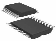
14-TSSOP (0.173, 4.40mm Width) - Number of Pins14
- Logic Level-High1.5V ~ 4.2V
- Logic Level-Low0.5V ~ 1.8V
- Operating Temperature
The operating temperature is the range of ambient temperature within which a power supply, or any other electrical equipment, operate in. This ranges from a minimum operating temperature, to a peak or maximum operating temperature, outside which, the power supply may fail.
-40°C~125°C - Packaging
Semiconductor package is a carrier / shell used to contain and cover one or more semiconductor components or integrated circuits. The material of the shell can be metal, plastic, glass or ceramic.
Tape & Reel (TR) - Series
In electronic components, the "Series" refers to a group of products that share similar characteristics, designs, or functionalities, often produced by the same manufacturer. These components within a series typically have common specifications but may vary in terms of voltage, power, or packaging to meet different application needs. The series name helps identify and differentiate between various product lines within a manufacturer's catalog.
74HC - Published1999
- JESD-609 Code
The "JESD-609 Code" in electronic components refers to a standardized marking code that indicates the lead-free solder composition and finish of electronic components for compliance with environmental regulations.
e4 - Part Status
Parts can have many statuses as they progress through the configuration, analysis, review, and approval stages.
Active - Moisture Sensitivity Level (MSL)
Moisture Sensitivity Level (MSL) is a standardized rating that indicates the susceptibility of electronic components, particularly semiconductors, to moisture-induced damage during storage and the soldering process, defining the allowable exposure time to ambient conditions before they require special handling or baking to prevent failures
1 (Unlimited) - Number of Terminations14
- Voltage - Supply
Voltage - Supply refers to the range of voltage levels that an electronic component or circuit is designed to operate with. It indicates the minimum and maximum supply voltage that can be applied for the device to function properly. Providing supply voltages outside this range can lead to malfunction, damage, or reduced performance. This parameter is critical for ensuring compatibility between different components in a circuit.
2V~6V - Terminal Position
In electronic components, the term "Terminal Position" refers to the physical location of the connection points on the component where external electrical connections can be made. These connection points, known as terminals, are typically used to attach wires, leads, or other components to the main body of the electronic component. The terminal position is important for ensuring proper connectivity and functionality of the component within a circuit. It is often specified in technical datasheets or component specifications to help designers and engineers understand how to properly integrate the component into their circuit designs.
DUAL - Terminal Form
Occurring at or forming the end of a series, succession, or the like; closing; concluding.
GULL WING - Peak Reflow Temperature (Cel)
Peak Reflow Temperature (Cel) is a parameter that specifies the maximum temperature at which an electronic component can be exposed during the reflow soldering process. Reflow soldering is a common method used to attach electronic components to a circuit board. The Peak Reflow Temperature is crucial because it ensures that the component is not damaged or degraded during the soldering process. Exceeding the specified Peak Reflow Temperature can lead to issues such as component failure, reduced performance, or even permanent damage to the component. It is important for manufacturers and assemblers to adhere to the recommended Peak Reflow Temperature to ensure the reliability and functionality of the electronic components.
260 - Number of Functions3
- Supply Voltage
Supply voltage refers to the electrical potential difference provided to an electronic component or circuit. It is crucial for the proper operation of devices, as it powers their functions and determines performance characteristics. The supply voltage must be within specified limits to ensure reliability and prevent damage to components. Different electronic devices have specific supply voltage requirements, which can vary widely depending on their design and intended application.
5V - Terminal Pitch
The center distance from one pole to the next.
0.65mm - Time@Peak Reflow Temperature-Max (s)
Time@Peak Reflow Temperature-Max (s) refers to the maximum duration that an electronic component can be exposed to the peak reflow temperature during the soldering process, which is crucial for ensuring reliable solder joint formation without damaging the component.
30 - Base Part Number
The "Base Part Number" (BPN) in electronic components serves a similar purpose to the "Base Product Number." It refers to the primary identifier for a component that captures the essential characteristics shared by a group of similar components. The BPN provides a fundamental way to reference a family or series of components without specifying all the variations and specific details.
74HC10 - Pin Count
a count of all of the component leads (or pins)
14 - Number of Outputs1
- Operating Supply Voltage
The voltage level by which an electrical system is designated and to which certain operating characteristics of the system are related.
5V - Supply Voltage-Max (Vsup)
The parameter "Supply Voltage-Max (Vsup)" in electronic components refers to the maximum voltage that can be safely applied to the component without causing damage. It is an important specification to consider when designing or using electronic circuits to ensure the component operates within its safe operating limits. Exceeding the maximum supply voltage can lead to overheating, component failure, or even permanent damage. It is crucial to adhere to the specified maximum supply voltage to ensure the reliable and safe operation of the electronic component.
6V - Supply Voltage-Min (Vsup)
The parameter "Supply Voltage-Min (Vsup)" in electronic components refers to the minimum voltage level required for the component to operate within its specified performance range. This parameter indicates the lowest voltage that can be safely applied to the component without risking damage or malfunction. It is crucial to ensure that the supply voltage provided to the component meets or exceeds this minimum value to ensure proper functionality and reliability. Failure to adhere to the specified minimum supply voltage may result in erratic behavior, reduced performance, or even permanent damage to the component.
2V - Load Capacitance
the amount of capacitance measured or computed across the crystal terminals on the PCB. Frequency Tolerance. Frequency tolerance refers to the allowable deviation from nominal, in parts per million (PPM), at a specific temperature, usually +25°C.
50pF - Output Current
The rated output current is the maximum load current that a power supply can provide at a specified ambient temperature. A power supply can never provide more current that it's rated output current unless there is a fault, such as short circuit at the load.
25mA - Propagation Delay
the flight time of packets over the transmission link and is limited by the speed of light.
16 ns - Quiescent Current
The quiescent current is defined as the current level in the amplifier when it is producing an output of zero.
2μA - Turn On Delay Time
Turn-on delay, td(on), is the time taken to charge the input capacitance of the device before drain current conduction can start.
9 ns - Family
In electronic components, the parameter "Family" typically refers to a categorization or classification system used to group similar components together based on their characteristics, functions, or applications. This classification helps users easily identify and select components that meet their specific requirements. The "Family" parameter can include various subcategories such as resistors, capacitors, diodes, transistors, integrated circuits, and more. Understanding the "Family" of an electronic component can provide valuable information about its compatibility, performance specifications, and potential uses within a circuit or system. It is important to consider the "Family" parameter when designing or troubleshooting electronic circuits to ensure proper functionality and compatibility with other components.
HC/UH - Logic Function
In electronic components, the term "Logic Function" refers to the specific operation or behavior of a component based on its input signals. It describes how the component processes the input signals to produce the desired output. Logic functions are fundamental to digital circuits and are used to perform logical operations such as AND, OR, NOT, and XOR.Each electronic component, such as logic gates or flip-flops, is designed to perform a specific logic function based on its internal circuitry. By understanding the logic function of a component, engineers can design and analyze complex digital systems to ensure proper functionality and performance. Different logic functions can be combined to create more complex operations, allowing for the creation of sophisticated digital devices and systems.
NAND - Logic Type
Logic Type in electronic components refers to the classification of circuits based on the logical operations they perform. It includes types such as AND, OR, NOT, NAND, NOR, XOR, and XNOR, each defining the relationship between binary inputs and outputs. The logic type determines how the inputs affect the output state based on specific rules of Boolean algebra. This classification is crucial for designing digital circuits and systems, enabling engineers to select appropriate components for desired functionalities.
NAND Gate - Number of Gates
The number of gates per IC varies depending on the number of inputs per gate. Two?input gates are common, but if only a single input is required, such as in the 744 NOT(or inverter) gates, a 14 pin IC can accommodate 6 (or Hex) gates.
3 - Max Propagation Delay @ V, Max CL
The parameter "Max Propagation Delay @ V, Max CL" in electronic components refers to the maximum amount of time it takes for a signal to propagate through the component from input to output when operating at a specific voltage (V) and driving a maximum specified load capacitance (CL). This parameter is crucial in determining the speed and performance of the component in a circuit. A shorter propagation delay indicates faster signal processing and better overall performance. Designers use this parameter to ensure that signals can be transmitted and received within the required timing constraints in their electronic systems.
16ns @ 6V, 50pF - Length5mm
- Width4.4mm
- Radiation Hardening
Radiation hardening is the process of making electronic components and circuits resistant to damage or malfunction caused by high levels of ionizing radiation, especially for environments in outer space (especially beyond the low Earth orbit), around nuclear reactors and particle accelerators, or during nuclear accidents or nuclear warfare.
No - RoHS Status
RoHS means “Restriction of Certain Hazardous Substances” in the “Hazardous Substances Directive” in electrical and electronic equipment.
ROHS3 Compliant - Lead Free
Lead Free is a term used to describe electronic components that do not contain lead as part of their composition. Lead is a toxic material that can have harmful effects on human health and the environment, so the electronics industry has been moving towards lead-free components to reduce these risks. Lead-free components are typically made using alternative materials such as silver, copper, and tin. Manufacturers must comply with regulations such as the Restriction of Hazardous Substances (RoHS) directive to ensure that their products are lead-free and environmentally friendly.
Lead Free
74HC10 Functional Block Diagram

Logic symbol

IEC logic symbol
.png")
Logic diagram (one gate)
74HC10 Equivalent
| Model number | Manufacturer | Description |
| SN74HC10PWTE4 | Rochester Electronics LLC | NAND Gate, HC/UH Series, 3-Func, 3-Input, CMOS, PDSO14, GREEN, PLASTIC, TSSOP-14 |
| 74HC10PW,112 | NXP Semiconductors | 74HC(T)10 - Triple 3-input NAND gate TSSOP 14-Pin |
| SN74HC10PWRE4 | Texas Instruments | Triple 3-Input Positive-NAND Gates 14-TSSOP -40 to 85 |
| 74HC10PW-Q100J | Nexperia | 74HC10-Q100; 74HCT10-Q100 - Triple 3-input NAND gate@en-us TSSOP 14-Pin |
| SN74HC10QPWREP | Texas Instruments | Enhanced product 3-ch, 3-input, 2-V to 6-V NAND gates 14-TSSOP -40 to 125 |
| SN74HC10PW | Texas Instruments | 3-ch, 3-input, 2-V to 6-V NAND gates 14-TSSOP -40 to 85 |
| 74HC10PW-T | NXP Semiconductors | IC HC/UH SERIES, TRIPLE 3-INPUT NAND GATE, PDSO14, TSSOP-14, Gate |
| 935186290118 | Nexperia | NAND Gate, HC/UH Series, 3-Func, 3-Input, CMOS, PDSO14 |
| 935186290112 | NXP Semiconductors | IC HC/UH SERIES, TRIPLE 3-INPUT NAND GATE, PDSO14, TSSOP-14, Gate |
| MC74HC10ADTR2G | ON Semiconductor | Triple 3-Input NAND Gate, TSSOP-14, 2500-REEL |
Parts with Similar Specs
- ImagePart NumberManufacturerPackage / CaseNumber of PinsLogic FunctionPropagation DelaySupply VoltageQuiescent CurrentMountMoisture Sensitivity Level (MSL)View Compare
![74HC10PW,118]()
74HC10PW,118
14-TSSOP (0.173, 4.40mm Width)
14
NAND
16 ns
5 V
2 μA
Surface Mount
1 (Unlimited)
![SN74HC10PWR]()
14-TSSOP (0.173, 4.40mm Width)
14
NAND
16 ns
5 V
2 μA
Surface Mount
1 (Unlimited)
![SN74HC10QPWRG4Q1]()
14-TSSOP (0.173, 4.40mm Width)
14
NAND
16 ns
5 V
2 μA
Surface Mount
1 (Unlimited)
![SN74HC10PWE4]()
14-TSSOP (0.173, 4.40mm Width)
14
NAND
16 ns
5 V
2 μA
Surface Mount
1 (Unlimited)
![74HC11PW,118]()
14-TSSOP (0.173, 4.40mm Width)
14
AND, NAND
26 ns
5 V
2 μA
Surface Mount
1 (Unlimited)


74HC10 Package

Package
74HC10 Manufacturer
Nexperia is dedicated to Discretes, Logic and MOSFETs devices. This new company became independent at the beginning of 2017.
Nexperia is a leading expert in the high-volume production of essential semiconductors, components that are required by every electronic design in the world. The company's extensive portfolio includes diodes, bipolar transistors, ESD protection devices, MOSFETs, GaN FETs and analog & logic ICs. With decades of experience in supplying to the world's leading companies, Nexperia has over 12,000 employees across Asia, Europe and the US. Nexperia creates efficient devices with best-in-class Quality. It has an extensive portfolio, produced to meet the stringent standards set by the Automotive industry. Its belief that efficiency wins is backed by flawless execution that meets the stringent requirements of the market and customers. Every Nexperia employee is tasked with the responsibility of maintaining Quality. Nexperia is a worldwide network built on passion and commitment to our work, belief in our goals and a drive to succeed.
Datasheet PDF
- PCN Packaging :
- Datasheets :
- RohsStatement :
Trend Analysis
What is the essential property of the 74HC10?
The 74HC10 is a Triple 3-input NAND Gate.
Can 74HCT replace 74HC series chips?
74HCT power supply voltage working range is 4.5V-5.5V, 74HC power supply voltage working range is 2V-6V. Therefore, when the power supply voltage of the application circuit chip is within the compatible range, it can be substituted.
 A Comprehensive Overview of the PIC18(L)F2X/4X/5XK42 Microcontroller Family: Architecture, Core Features, and Operation
29 February 2024262
 MT8870 DTMF Receiver: Pin Description, Price and Datasheet
16 August 20214357
 AVX TAJA106K016RNJ Datasheet Guide: Complete Tantalum Capacitor Specs
08 September 20251130
 TIP125 Darlington Transistor: Datasheet PDF, Pinout, Circuit
15 February 20226289
 TPS2557DRBT Dual Timer IC: Features, Pinout, and Datasheet
15 April 20222473
 PESD2CAN TVS Diode: SOT-23, CAN Bus, Datasheet and Pinout
16 February 20224717
 2SB817 PNP Power Transistor: B817 Power Transistor, Datasheet pdf and Equivalent
15 December 202113200
 93C46 EEPROM: Features, Pinout, and Datasheet
17 January 202211999
 RVDT(Rotary Variable Differential Transformer) Basics
02 February 202120605
 Basic Guidelines for Mixed-Signal PCB Layout Design
15 March 20246818
 The Understanding to Autonomous Driving Sensor
10 November 20211339
 What is a Hard Disk Drive (HDD)?
31 May 20215500
 Designing Application-Specific Integrated Circuits
07 March 20252308
 What is Oscilloscope?
24 September 20218049
 What is a Ground Fault Circuit Interrupter?
27 March 20255614
 Shift Registers Made Simple for New Learners
15 July 20253695
Nexperia USA Inc.
In Stock: 3438
Minimum: 1 Multiples: 1
Qty
Unit Price
Ext Price
1
$0.371215
$0.37
10
$0.350203
$3.50
100
$0.330380
$33.04
500
$0.311679
$155.84
1000
$0.294037
$294.04
Not the price you want? Send RFQ Now and we'll contact you ASAP.
Inquire for More Quantity
![74HCT86D,653]() 74HCT86D,653
74HCT86D,653Nexperia USA Inc.
![74HC04D,653]() 74HC04D,653
74HC04D,653Nexperia USA Inc.
![74HC32D,653]() 74HC32D,653
74HC32D,653Nexperia USA Inc.
![74AHC1G32GW,125]() 74AHC1G32GW,125
74AHC1G32GW,125Nexperia USA Inc.
![HEF4093BT,653]() HEF4093BT,653
HEF4093BT,653Nexperia USA Inc.
![74HC02D,653]() 74HC02D,653
74HC02D,653Nexperia USA Inc.
![74LVC14APW,118]() 74LVC14APW,118
74LVC14APW,118Nexperia USA Inc.
![74AUP1G08GX,125]() 74AUP1G08GX,125
74AUP1G08GX,125Nexperia USA Inc.
![74LVC1G14GV,125]() 74LVC1G14GV,125
74LVC1G14GV,125Nexperia USA Inc.
![HEF4069UBT,653]() HEF4069UBT,653
HEF4069UBT,653Nexperia USA Inc.


