
 Product
 Brand
Brand Articles
 Tools
Tools
AD4004 16-Bit 1 MSPS SAR ADC: Datasheet, Performance, and Integration Deep Dive

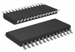
16 Bit 0.5mm ADC AD4004 1.8V 10-TFSOP, 10-MSOP (0.118, 3.00mm Width)
Unit Price: $16.238726
Ext Price: $16.24


16 Bit 0.5mm ADC AD4004 1.8V 10-TFSOP, 10-MSOP (0.118, 3.00mm Width)
Master the AD4004 16-bit 1 MSPS SAR ADC. Explore datasheet specs, pinouts, and overvoltage solutions for precision data acquisition. Start your design today.
- Executive Summary: What is the AD4004?
- 1. Technical Specifications & Performance Analysis
- 2. Pinout, Package, and Configuration
- 3. Design & Integration Guide (For Engineers & Makers)
- 4. Typical Applications & Use Cases
- 5. Alternatives and Cross-Reference Guide
- 6. Frequently Asked Questions (FAQ)
- 7. Resources
- Specifications
- Datasheet PDF
Executive Summary: What is the AD4004?
The AD4004 is a 16-bit, 1 MSPS precision pseudo-differential successive approximation register (SAR) analog-to-digital converter (ADC) designed for high-accuracy data acquisition systems. Manufactured by Analog Devices, it is engineered to reduce signal chain power consumption and complexity while maintaining industry-leading throughput and accuracy.
Market Position: High-performance, precision analog-to-digital converter ideal for low-power, high-accuracy applications.
Top Features: Easy Drive technology for signal chain flexibility, High-Z mode for reduced settling requirements, and a built-in input overvoltage protection clamp (sinks up to 50 mA).
Primary Audience: Design engineers and procurement managers developing precision instrumentation, medical equipment, and automated test equipment (ATE).
Supply Status: Active. (Verify exact packaging and reel quantities with your electronics distributor).
1. Technical Specifications & Performance Analysis
1.1 Core Architecture (CPU/Logic/Power)
At its core, the AD4004 utilizes a highly efficient SAR (Successive Approximation Register) architecture. The ADC features a pseudo-differential input, meaning it digitizes the voltage difference between the IN+ and IN− pins while rejecting common-mode noise.
A standout feature of this architecture is the Easy Drive technology and High-Z mode. These features significantly reduce the signal chain settling requirements, allowing engineers to pair the ADC with lower-power, lower-bandwidth driving amplifiers, ultimately reducing overall BOM cost and system power consumption. Furthermore, the fast conversion phase extends the ADC acquisition time, easing the burden on the analog front end.
1.2 Key Electrical Characteristics
When evaluating the AD4004 datasheet, power and precision are the primary drivers for component selection:
Resolution: 16-Bit (Guaranteed no missing codes)
Throughput: 1 MSPS
Integral Nonlinearity (INL): ±1.0 LSB maximum
Signal-to-Noise Ratio (SNR): 93 dB (at fIN = 1 kHz, VREF = 5 V)
Supply Voltage (VDD): 1.71 V to 1.89 V
Reference Voltage (VREF): 2.4 V to 5.1 V
Power Consumption: Extremely low at 7 mW at 1 MSPS
1.3 Interfaces and Connectivity
The AD4004 communicates via a versatile serial interface that is compatible with SPI, QSPI, MICROWIRE, and DSP protocols. This ensures seamless integration with a wide variety of microcontrollers (like STM32 or ESP32), DSPs, and FPGAs.
2. Pinout, Package, and Configuration
2.1 Pin Configuration Guide
While the exact pinout depends on the chosen package, standard integration involves several critical nodes:
VDD & GND: Core power supply (1.8V nominal) and system ground.
VREF: Reference voltage input (2.4 V to 5.1 V). This strictly dictates the ADC's conversion scale.
IN+ / IN-: The pseudo-differential analog inputs.
SDI, SDO, SCK, CNV: The standard 4-wire SPI communication and conversion control pins.
2.2 Naming Convention & Ordering Codes
Understanding the Part Numbers:Analog Devices uses specific suffixes to denote package type, temperature grade, and packaging method (e.g., AD4004BRMZ-RL7). - B: Typically denotes the performance grade.
- RM/CP: Denotes the package style (e.g., MSOP or LFCSP).
- -RL7: Indicates Tape and Reel packaging (crucial for Procurement Managers scheduling machine assembly).
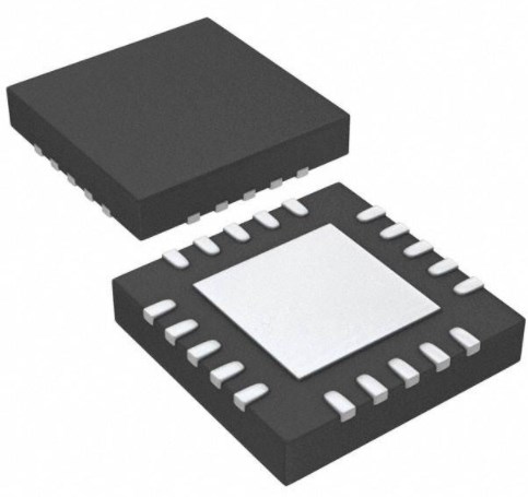
2.3 Available Packages
| Package Type | Dimensions | Common Use Case |
|---|---|---|
| 10-Lead MSOP | 3.00 mm × 4.90 mm | Hand-soldering friendly; standard prototyping and production. |
| 10-Lead LFCSP | 3.00 mm × 3.00 mm | Space-constrained designs; machine assembly only. |
(Note: Always consult the latest AD4004 datasheet for exact mechanical dimensions and thermal pad requirements).
3. Design & Integration Guide (For Engineers & Makers)
Pro Tip: Always verify pin compatibility and SPI timing configurations before migrating from older 16-bit ADCs to the AD4004.
3.1 Hardware Implementation
Bypass Capacitors: Place a high-quality 10 µF or 1 µF ceramic capacitor as close to the VREF and VDD pins as possible to minimize high-frequency noise.
PCB Layout: A solid ground plane is mandatory. Keep digital traces (SCK, SDO) physically separated from sensitive analog inputs (IN+, IN-) to prevent crosstalk.
Thermal Management: Given its ultra-low power consumption (7 mW), the AD4004 does not require a heatsink under standard operating conditions.
3.2 Common Design Challenges
Issue: SPI Interface Timing Issues Symptom: Users report receiving incorrect hex values or offsets when reading the ADC due to tricky SPI timing requirements. Fix: Configure your microcontroller's SPI with CPOL=0 and CPHA=0. Ensure data is latched strictly on the SCK rising edge, and carefully follow the datasheet timing specs for the conversion (CNV) pulse.
Issue: Amplifier Headroom and Footroom Symptom: In single-supply systems, the driving amplifier cannot always drive the full ADC input range all the way to ground or the maximum reference voltage. Fix: Enable the AD4004's built-in input span compression feature. This preserves the full ADC code range without needing a negative power supply for the driving amplifier.
Issue: Input Overvoltage Damage Symptom: Amplifier rails greater than VREF can violate the ADC's input voltage range, disturbing the reference or permanently damaging the part. Fix: Rely on the AD4004's robust built-in input overvoltage protection clamp. It safely sinks up to 50 mA, eliminating the need for external protection diodes and saving board space.
4. Typical Applications & Use Cases
Watch Tutorial: AD4004
The AD4004 is highly versatile, with primary applications including: - Automated test equipment (ATE) - Machine automation - Medical equipment (e.g., patient monitoring) - Battery-powered equipment - Precision data acquisition systems - Instrumentation and control systems
4.1 Real-World Example: Precision Medical Instrumentation
In medical equipment like ECG monitors, precision and battery life are paramount. The AD4004 fits perfectly here because its High-Z mode allows it to be driven by lower-power instrumentation amplifiers. The 16-bit resolution captures minute physiological signals, while the 7 mW power consumption ensures the device can run for extended periods on battery power.
5. Alternatives and Cross-Reference Guide
When managing BOMs, comparing price vs performance is critical. If the AD4004 is out of stock or over-specced for your project, consider these alternatives:
AD4000: A pin-compatible sibling from Analog Devices offering 16-bit resolution but at a higher throughput of 2 MSPS. Ideal if you need faster sampling.
AD4008: Another pin-compatible option in the same family, offering a lower throughput (500 kSPS) for more cost-sensitive, lower-speed applications.
ADAS3022: A complete 16-bit data acquisition system (DAS) from ADI that includes an integrated programmable gain amplifier (PGA), useful if you want to eliminate the external driving amplifier entirely.
Texas Instruments ADS8860: A direct competitor offering 16-bit, 1 MSPS SAR performance. A strong equivalent to evaluate for cross-referencing and supply chain resilience.
6. Frequently Asked Questions (FAQ)
Q: What is the difference between AD4004 and AD4000? A: Both are 16-bit precision SAR ADCs from Analog Devices, but the AD4004 operates at 1 MSPS, whereas the AD4000 operates at a faster 2 MSPS throughput.
Q: Is the AD4004 suitable for battery-operated devices? A: Yes, it is highly recommended. It consumes only 7 mW at 1 MSPS, making it exceptionally well-suited for battery-powered and portable equipment.
Q: How do I program/configure the AD4004? A: The AD4004 is configured via its SPI-compatible serial interface. Features like High-Z mode and span compression can be enabled by writing to its internal configuration register.
Q: Does the AD4004 need external overvoltage protection? A: No. It features an internal input overvoltage protection clamp that can safely sink up to 50 mA, protecting the device from transient amplifier rail spikes.
Q: Where can I find the datasheet, schematic symbol, and library files for the AD4004? A: The official datasheet, CAD models (ECAD/MCAD), and schematic symbols can be downloaded directly from the Analog Devices website or your preferred component distributor.
7. Resources
Development Tools & Software: Analog Devices offers dedicated Evaluation Boards (e.g., EVAL-AD4004FMCZ) and the Analysis | Control | Evaluation (ACE) software to test the ADC's performance before committing to a custom PCB layout.
Specifications
Datasheet PDF
- Datasheets :
- ConflictMineralStatement :
 BMP085 Pressure Sensor: Datasheet, Pinout, BMP085 vs.BMP180
01 November 20212909
 TPS7A33: Regulator, Pinout, Circuit
30 March 20222590
 LD1117S50TR: Overview, applications and Datasheet
23 November 2023903
 Navigating the XA-H4 Single-Chip 16-bit Microcontroller: An In-depth Analysis
29 February 2024175
 ADM3053BRWZ CAN Bus Transceivers: 5.5 V, SOIC and ADM3053 CAN Stock
22 February 20222757
 AT28HC64B High-speed Parallel EEPROM: Pinout, Equivalent and Datasheet
09 March 20221789
 IRFB7545PBF Power MOSFET: IRFB7545PBF MOSFET Equivalent, Datasheet, Pinout
14 January 202213556
![NRF5340 VS NRF52840 Bluetooth LE NFC[FAQ]](https://res.utmel.com/Images/Article/c434c1d9-ae3e-4bca-8ee9-9c417d764907.jpg) NRF5340 VS NRF52840 Bluetooth LE NFC[FAQ]
NRF5340 VS NRF52840 Bluetooth LE NFC[FAQ]12 March 202213053
 What is latch?
28 March 20256888
 VRLA Battery: Working Principle, Capacity and Maintenance
12 March 202110644
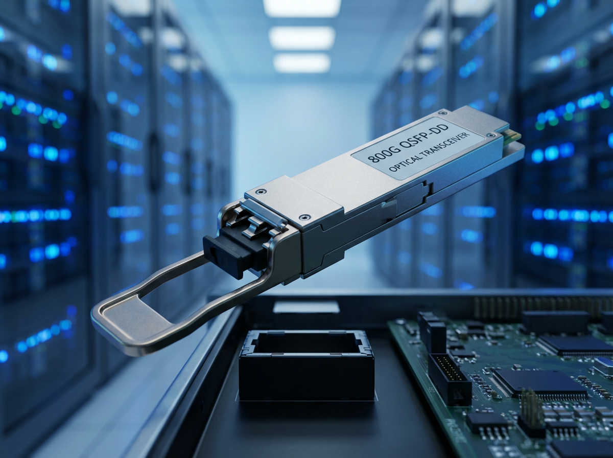 800G Optical Transceivers: The Guide for AI Data Centers
24 December 202510449
 A brief Analysis of the 555 Timer Circuit and its Project Applications
15 March 20243292
 Intel Launches First-of-its-Kind Semiconductor Technician Certificate Program to Address Workforce Shortage
28 September 20233599
 Analysis of Resistors in Series and Parallel
12 June 202621275
 Introduction to Photonic Integrated Circuits and PIC Technology
22 October 202515062
 2026 Passive Components Market Update: Sourcing Tactics Amid Price Hikes and Lead Time Extensions
15 June 20262275
Analog Devices Inc.
In Stock: 16
Minimum: 1 Multiples: 1
Qty
Unit Price
Ext Price
1
$16.238726
$16.24
10
$15.319553
$153.20
100
$14.452408
$1,445.24
500
$13.634348
$6,817.17
1000
$12.862592
$12,862.59
Not the price you want? Send RFQ Now and we'll contact you ASAP.
Inquire for More Quantity
![ADV7513BSWZ]() ADV7513BSWZ
ADV7513BSWZAnalog Devices, Inc.
![AD9877ABSZ]() AD9877ABSZ
AD9877ABSZAnalog Devices, Inc.
![LTC2245CUH#TRPBF]() LTC2245CUH#TRPBF
LTC2245CUH#TRPBFLinear Technology/Analog Devices
![AD7791BRMZ-REEL]() AD7791BRMZ-REEL
AD7791BRMZ-REELAnalog Devices Inc.
![AD7799BRUZ-REEL]() AD7799BRUZ-REEL
AD7799BRUZ-REELAnalog Devices Inc.
![AD7190BRUZ-REEL]() AD7190BRUZ-REEL
AD7190BRUZ-REELAnalog Devices Inc.
![AD7705BRZ-REEL]() AD7705BRZ-REEL
AD7705BRZ-REELAnalog Devices Inc.
![AD7175-2BRUZ-RL7]() AD7175-2BRUZ-RL7
AD7175-2BRUZ-RL7Analog Devices Inc.
![AD7192BRUZ-REEL]() AD7192BRUZ-REEL
AD7192BRUZ-REELAnalog Devices Inc.
![AD9283BRSZ-RL100]() AD9283BRSZ-RL100
AD9283BRSZ-RL100Analog Devices Inc.


