Product
 Brand
Brand Articles
 Tools
Tools
AD8361 2.5 GHz RF Power Detector: Precision Datasheet, Pinout, and Implementation Analysis


IC PWR DETECTOR 2.5GHZ 8MSOP
The AD8361 is a 2.5 GHz mean-responding RF power detector from Analog Devices. Explore specs, pinout, and design tips for precise CDMA/QAM power measurement.
- Executive Summary: What is the AD8361?
- 1. Technical Specifications & Performance Analysis
- 2. Pinout, Package, and Configuration
- 3. Design & Integration Guide
- 4. Typical Applications & Use Cases
- 5. Alternatives and Cross-Reference Guide
- 6. Frequently Asked Questions (FAQ)
- 7. Resources
- Specifications
- Datasheet PDF
Executive Summary: What is the AD8361?
The AD8361 is a TruPwr™ mean-responding power detector designed for high-frequency signal chains, providing a linear-in-voltage DC output proportional to the RMS level of an RF input signal up to 2.5 GHz. It is specifically engineered to measure complex modulation waveforms like CDMA, W-CDMA, and QAM where peak-to-average ratios vary.
Market Position: Industry-standard, high-precision RMS-responding detector for infrastructure and portable RF.
Top Features: Calibrated RMS response, ultra-low power consumption (3.3 mW), and excellent temperature stability.
Primary Audience: RF Design Engineers, Wireless Infrastructure Architects, and Telecommunications Procurement Managers.
Supply Status: Active (Widely available through authorized distribution).
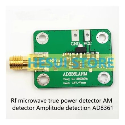
1. Technical Specifications & Performance Analysis
1.1 Core Architecture: Mean-Responding Detection
Unlike simple diode detectors that often respond to peak voltage, the AD8361 utilizes a proprietary square-law detection technique. This "mean-responding" architecture ensures that the output remains stable regardless of the crest factor of the input signal, making it indispensable for modern digital modulation schemes.
1.2 Key Electrical Characteristics
The AD8361 is optimized for low-voltage, battery-efficient operation without sacrificing dynamic range.
| Parameter | Specification Value |
|---|---|
| Operating Frequency | LF (Low Frequency) to 2.5 GHz |
| Supply Voltage Range | 2.7 V to 5.5 V |
| Quiescent Current | 1.1 mA (3.3 mW at 3 V) |
| Conversion Gain | 7.5 V/V rms |
| Input Range | Up to 30 dB at 2.5 GHz |
| Operating Temperature | -40°C to +85°C |
1.3 Interfaces and Connectivity
The device features a high-impedance RF input (RFIN) and a buffered voltage output (VOUT). It includes a power-down (PWDN) pin compatible with standard CMOS logic, reducing current draw to less than 1 µA when inactive.
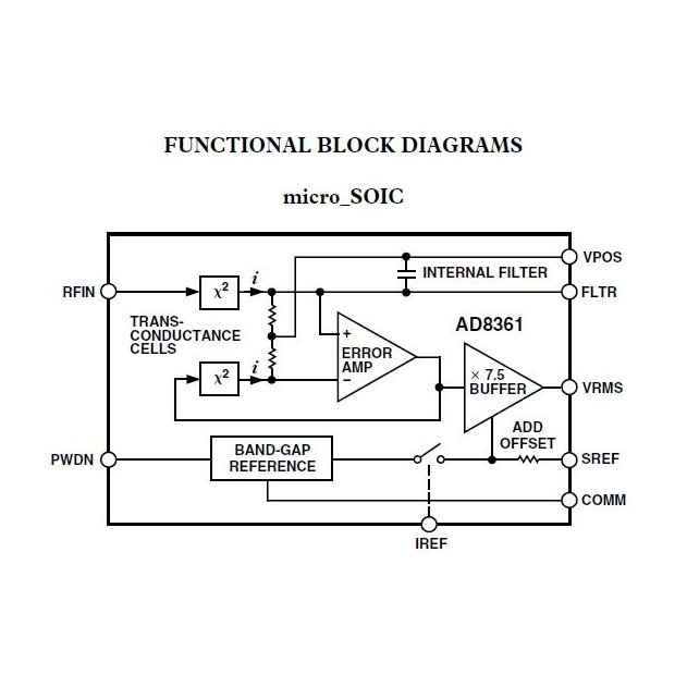
2. Pinout, Package, and Configuration
2.1 Pin Configuration Guide
The AD8361 is typically available in 6-lead SOT-23 and 8-lead MSOP packages.
RFIN: RF Input signal.
COMM: Device Ground.
PWDN: Logic high to power down the device.
FLTR: Connection for external filter capacitor to adjust averaging time constant.
VOUT: Linear-in-voltage DC output.
VPOS: Positive Supply Rail (2.7V to 5.5V).
2.2 Naming Convention & Ordering Codes
AD8361ARM: MSOP Package.
AD8361ARTZ: SOT-23 Package (Lead-free).
Suffix -REEL7: Indicates 7-inch tape and reel packaging for automated assembly.
2.3 Available Packages
| Package Type | Dimensions | Common Use Case |
|---|---|---|
| SOT-23-6 | 2.9mm x 1.6mm | Space-constrained mobile handsets / Hand-soldering friendly |
| MSOP-8 | 3.0mm x 3.0mm | Industrial RF modules / Precision instrumentation |
3. Design & Integration Guide
Pro Tip: To maintain accuracy at high frequencies, keep the input trace impedance at 50 Ω and minimize the distance between the decoupling capacitors and the VPOS pin.
3.1 Hardware Implementation
Bypass Capacitors: Use a combination of a 100 pF and a 0.1 µF capacitor on the VPOS pin to filter both high-frequency noise and low-frequency ripple.
Filter Capacitor (CFLTR): The internal averaging resistor is 250 Ω. Adding an external capacitor to the FLTR pin allows the designer to trade off response time for lower output ripple.
PCB Layout: Use a solid ground plane. The RFIN trace should be a microstrip or stripline designed for 50 Ω characteristic impedance.
3.2 Common Design Challenges
Issue: Low Input Power Inaccuracy
Cause: The AD8361 exhibits a non-zero output offset (up to 200 mV) even with no signal.
Fix: Implement a software-based DC offset calibration. Measure the "dark" voltage at PWDN=Low and subtract it from active readings.
Issue: Impedance Mismatch Reflections
Cause: High VSWR at the input can cause "triple travel" ripples in the response curve.
Fix: Place a 3 dB coaxial attenuator or a resistive pad directly at the RFIN port to improve the match.
4. Typical Applications & Use Cases
Watch Tutorial: AD8361
4.1 Real-World Example: W-CDMA Transmitter Control
In a W-CDMA base station, the AD8361 monitors the output of the Power Amplifier (PA). Because W-CDMA has a high peak-to-average power ratio (PAPR), a standard diode detector would provide inaccurate readings. The AD8361 provides a precise RMS voltage to the system microcontroller, allowing for real-time AGC (Automatic Gain Control) adjustments to maintain spectral mask compliance.
5. Alternatives and Cross-Reference Guide
Direct Replacement (Enhanced): ADL5501 (Similar footprint, improved dynamic range).
True RMS Upgrade: AD8362 (Provides 65 dB dynamic range, linear-in-dB output).
Higher Frequency: ADL5902 (Operates up to 9 GHz for 5G/WiFi-6 applications).
6. Frequently Asked Questions (FAQ)
Q: What is the difference between AD8361 and AD8313?
A: The AD8361 is a linear-in-voltage RMS detector (best for precise power measurement of complex waves), while the AD8313 is a logarithmic detector (best for wide dynamic range RSSI).
Q: Can the AD8361 be used for pulse detection?
A: Yes, provided the pulse width is longer than the averaging time constant set by the FLTR capacitor.
Q: Is the AD8361 suitable for battery-operated devices?
A: Absolutely. Its 1.1 mA current draw and sub-1µA power-down mode make it ideal for portable gear.
7. Resources
Evaluation Board: AD8361-EVALZ
CAD Models: Available in Altium, Eagle, and KiCad formats via SnapEDA/Ultra Librarian.
Specifications
Datasheet PDF
- Datasheets :
- PCN Assembly/Origin :
- ConflictMineralStatement :
 NTE987 Operational Amplifier: Datasheet, Pinout and Equivalent
16 September 20212741
 LTC7545ABSW#TRPBF Digital to Analog Converter: Product Overview and Applications
06 March 2024226
 TMC2208 vs. TMC2209: What Differences is between them?
22 February 202242168
 PMEG4010BEA Diode: 1A, SOD323, MEGA Schottky Barrier Rectifier
24 February 2022636
 CL220 Regulator: Datasheet, Application, Circuit
06 September 2021679
 LM317 vs IRFZ44N Mosfet: Who works better?
03 August 202213754
 LTC3780 Buck-Boost Controller: Alternative, Price and Datasheet
21 July 20216201
 INA219 Current Shunt and Power Monitor: Architecture & Design Guide
17 January 20263639
 HIKSEMI Authorized Distributor | UTMEL Electronics
15 November 20234305
 Basis of Fiber Optic and Fiber Optic Communication
22 October 20215504
 Semiconductor Equipment Industry Research
25 March 20245157
 Analyzing the Latest Electronic Components Trends and Their Functions 2023 – 2024
21 July 20253290
 What is Universal Serial Bus (USB)?
12 June 202613307
 Understanding the Basics of I2C Interface Controllers
11 June 20251950
 VRLA Battery: Working Principle, Capacity and Maintenance
12 March 202111044
 Ten Smart Sensor Technology Trends for IoT Applications
20 November 20216719
Analog Devices Inc.
In Stock
United States
China
Canada
Japan
Russia
Germany
United Kingdom
Singapore
Italy
Hong Kong(China)
Taiwan(China)
France
Korea
Mexico
Netherlands
Malaysia
Austria
Spain
Switzerland
Poland
Thailand
Vietnam
India
United Arab Emirates
Afghanistan
Åland Islands
Albania
Algeria
American Samoa
Andorra
Angola
Anguilla
Antigua & Barbuda
Argentina
Armenia
Aruba
Australia
Azerbaijan
Bahamas
Bahrain
Bangladesh
Barbados
Belarus
Belgium
Belize
Benin
Bermuda
Bhutan
Bolivia
Bonaire, Sint Eustatius and Saba
Bosnia & Herzegovina
Botswana
Brazil
British Indian Ocean Territory
British Virgin Islands
Brunei
Bulgaria
Burkina Faso
Burundi
Cabo Verde
Cambodia
Cameroon
Cayman Islands
Central African Republic
Chad
Chile
Christmas Island
Cocos (Keeling) Islands
Colombia
Comoros
Congo
Congo (DRC)
Cook Islands
Costa Rica
Côte d’Ivoire
Croatia
Cuba
Curaçao
Cyprus
Czechia
Denmark
Djibouti
Dominica
Dominican Republic
Ecuador
Egypt
El Salvador
Equatorial Guinea
Eritrea
Estonia
Eswatini
Ethiopia
Falkland Islands
Faroe Islands
Fiji
Finland
French Guiana
French Polynesia
Gabon
Gambia
Georgia
Ghana
Gibraltar
Greece
Greenland
Grenada
Guadeloupe
Guam
Guatemala
Guernsey
Guinea
Guinea-Bissau
Guyana
Haiti
Honduras
Hungary
Iceland
Indonesia
Iran
Iraq
Ireland
Isle of Man
Israel
Jamaica
Jersey
Jordan
Kazakhstan
Kenya
Kiribati
Kosovo
Kuwait
Kyrgyzstan
Laos
Latvia
Lebanon
Lesotho
Liberia
Libya
Liechtenstein
Lithuania
Luxembourg
Macao(China)
Madagascar
Malawi
Maldives
Mali
Malta
Marshall Islands
Martinique
Mauritania
Mauritius
Mayotte
Micronesia
Moldova
Monaco
Mongolia
Montenegro
Montserrat
Morocco
Mozambique
Myanmar
Namibia
Nauru
Nepal
New Caledonia
New Zealand
Nicaragua
Niger
Nigeria
Niue
Norfolk Island
North Korea
North Macedonia
Northern Mariana Islands
Norway
Oman
Pakistan
Palau
Palestinian Authority
Panama
Papua New Guinea
Paraguay
Peru
Philippines
Pitcairn Islands
Portugal
Puerto Rico
Qatar
Réunion
Romania
Rwanda
Samoa
San Marino
São Tomé & Príncipe
Saudi Arabia
Senegal
Serbia
Seychelles
Sierra Leone
Sint Maarten
Slovakia
Slovenia
Solomon Islands
Somalia
South Africa
South Sudan
Sri Lanka
St Helena, Ascension, Tristan da Cunha
St. Barthélemy
St. Kitts & Nevis
St. Lucia
St. Martin
St. Pierre & Miquelon
St. Vincent & Grenadines
Sudan
Suriname
Svalbard & Jan Mayen
Sweden
Syria
Tajikistan
Tanzania
Timor-Leste
Togo
Tokelau
Tonga
Trinidad & Tobago
Tunisia
Turkey
Turkmenistan
Turks & Caicos Islands
Tuvalu
U.S. Outlying Islands
U.S. Virgin Islands
Uganda
Ukraine
Uruguay
Uzbekistan
Vanuatu
Vatican City
Venezuela
Wallis & Futuna
Yemen
Zambia
Zimbabwe
![AD8361ARMZ]() AD8361ARMZ
AD8361ARMZAnalog Devices Inc.
![AD8313ARMZ]() AD8313ARMZ
AD8313ARMZAnalog Devices Inc.
![AD8319ACPZ-R7]() AD8319ACPZ-R7
AD8319ACPZ-R7Analog Devices Inc.
![ADL5902ACPZ-R7]() ADL5902ACPZ-R7
ADL5902ACPZ-R7Analog Devices Inc.
![AD8362ARUZ-REEL7]() AD8362ARUZ-REEL7
AD8362ARUZ-REEL7Analog Devices Inc.
![ADL5513ACPZ-R7]() ADL5513ACPZ-R7
ADL5513ACPZ-R7Analog Devices Inc.
![AD8302ARUZ]() AD8302ARUZ
AD8302ARUZAnalog Devices Inc.
![LTC5507ES6#TRMPBF]() LTC5507ES6#TRMPBF
LTC5507ES6#TRMPBFAnalog Devices
![AD8362ARUZ]() AD8362ARUZ
AD8362ARUZAnalog Devices Inc.