
 Product
 Brand
Brand Articles
 Tools
Tools
AD8367 500 MHz Variable Gain Amplifier: Datasheet, Pinout, and AGC Design Analysis


Amplifier
Explore the AD8367 45 dB Variable Gain Amplifier. Features 500 MHz bandwidth and X-AMP architecture for AGC loops. View specs and optimize your RF design today.
- Executive Summary: What is the AD8367?
- 1. Technical Specifications & Performance Analysis
- 2. Pinout, Package, and Configuration
- 3. Design & Integration Guide (For Engineers & Makers)
- 4. Typical Applications & Use Cases
- 5. Alternatives and Cross-Reference Guide
- 6. Frequently Asked Questions (FAQ)
- 7. Resources
- Specifications
- Datasheet PDF
Executive Summary: What is the AD8367?
The AD8367 is a high-performance 45 dB variable gain amplifier (VGA) designed for linear-in-dB gain control in applications ranging from low frequencies up to 500 MHz. It utilizes Analog Devices’ proprietary X-AMP® architecture to provide precise gain scaling and high-speed operation.
Market Position: High-performance, industry-standard VGA for RF/IF signal chains.
Top Features: 45 dB dynamic range (-2.5 dB to +42.5 dB), 500 MHz bandwidth, and an integrated square-law detector for AGC loops.
Primary Audience: Ideal for RF design engineers, telecommunications infrastructure developers, and broadband equipment manufacturers.
Supply Status: Active; widely available through major electronics distributors.
1. Technical Specifications & Performance Analysis
The AD8367 is a dictionary-style example of a Variable Gain Amplifier (VGA) designed for IF (Intermediate Frequency) stages in wireless receivers.
1.1 Core Architecture (X-AMP)
{{SECTION_1_OVERVIEW}} The AD8367 is built on the X-AMP (Exponential Amplifier) architecture. Unlike traditional VGAs that vary the gain of the active stage, the X-AMP uses a precision 200 Ω passive resistive attenuator followed by a fixed-gain feedback amplifier. This ensures that the amplifier always operates with a constant bandwidth and high linearity across the majority of its control range.
1.2 Key Electrical Characteristics
Engineers must account for the following power and performance metrics during the BOM selection process:
Gain Range: Total of 45 dB (-2.5 dB to +42.5 dB).
Bandwidth: A robust 500 MHz (3 dB cutoff), making it suitable for high-speed data I/O and broadband access.
Operating Voltage: Single-supply operation from 2.7 V to 5.5 V, facilitating integration into both legacy 5V systems and modern low-power 3.3V rails.
Current Consumption: Typically 26 mA quiescent current, balancing performance with thermal efficiency.
Linearity: Output Third Order Intercept (OIP3) of +20 dBV at 100 MHz, ensuring minimal signal distortion in crowded spectrums.
1.3 Interfaces and Connectivity
The device features a "Linear-in-dB" control interface. The gain is controlled by an analog voltage applied to the GAIN pin, scaled at 20 mV/dB. It also includes a MODE pin that allows the user to toggle between "Gain Up" (positive slope) and "Gain Down" (negative slope) control, providing flexibility for different feedback loop polarities.
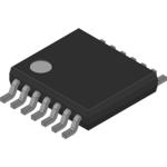
2. Pinout, Package, and Configuration
The AD8367's layout is optimized for high-frequency signal integrity, keeping input and output pins separated by ground pins to minimize crosstalk.
2.1 Pin Configuration Guide
VIN (Pin 13): Resistive ground-referenced input with a nominal 200 Ω impedance.
VOUT (Pin 5): High-speed output signal.
GAIN (Pin 11): Analog gain control input.
DETO (Pin 4): Output of the integrated square-law detector; used to drive the GAIN pin in AGC applications.
MODE (Pin 12): Sets the gain slope (High for positive, Low for negative).
VPOS / COMM: Power supply and ground pins.
2.2 Naming Convention & Ordering Codes
The most common ordering code is the AD8367ARUZ, where "ARU" designates the TSSOP package and "Z" indicates a RoHS-compliant (lead-free) part. Procurement managers should verify the suffix to ensure compatibility with automated pick-and-place moisture sensitivity levels (MSL).
2.3 Available Packages
| Package Type | Dimensions | Common Use Case |
|---|---|---|
| TSSOP-14 | 4.4mm x 5.0mm | Standard PCB assembly; compact footprint for base stations. |
Note: The TSSOP-14 package is machine-assembly friendly but can be hand-soldered by experienced technicians using fine-tip irons or hot air stations.
3. Design & Integration Guide (For Engineers & Makers)
Pro Tip: Always use a solid ground plane. At 500 MHz, even a small parasitic inductance in the ground path can lead to instability.
3.1 Hardware Implementation
Bypass Capacitors: Use a combination of a 0.1 µF ceramic capacitor for low-frequency decoupling and a 100 pF capacitor placed as close as possible to the VPOS pin to filter high-frequency noise.
Input Matching: Since the input impedance is 200 Ω, matching networks (such as a 4:1 balun or LC network) may be required when interfacing with standard 50 μV RF systems.
Thermal Management: With a 26 mA draw at 5V, the device dissipates roughly 130 mW. While it does not usually require a dedicated heatsink, ensure sufficient copper area is connected to the COMM pins for heat dissipation.
3.2 Common Design Challenges
Issue: Noise Figure Degradation at Low Gain.
Fix: Because the X-AMP architecture attenuates the input before amplifying, the noise figure increases as gain decreases. To maintain a high SNR, place a Low-Noise Amplifier (LNA) before the AD8367.
Issue: Self-Excitation and Instability.
Fix: This often occurs near maximum control voltage. Ensure strict power supply decoupling and avoid long traces on the GAIN control line which can pick up stray EMI.
Issue: Cascading Gain Mismatch.
Fix: If +42.5 dB is too high for your second stage, use a fixed attenuator (e.g., 6 dB) between stages to keep the amplifiers within their linear operating regions.
4. Typical Applications & Use Cases
4.1 Real-World Example: Automatic Gain Control (AGC)
In a Cellular Base Station, the incoming signal strength varies wildly. The AD8367 is used as a "Complete IF AGC Amplifier." By connecting the DETO (Detector Output) pin back to the GAIN pin through a simple low-pass filter, the AD8367 automatically adjusts its gain to maintain a constant output power level, protecting the subsequent Analog-to-Digital Converter (ADC) from clipping.
5. Alternatives and Cross-Reference Guide
If the AD8367 is unavailable or does not meet specific requirements, consider these alternatives:
Direct Replacements (Analog Devices):
AD603: A classic VGA, though it has a lower bandwidth (90 MHz) compared to the AD8367.
AD8330: Offers a wider gain range and differential inputs, ideal for low-frequency applications.
Competitor Options (Texas Instruments):
VCA821: A wideband, voltage-controlled amplifier offering high bandwidth and similar gain-control characteristics.
LMH6515: A digital-controlled VGA if your design requires SPI/Parallel control instead of analog voltage.
6. Frequently Asked Questions (FAQ)
Q: What is the difference between AD8367 and AD603?A: The AD8367 supports up to 500 MHz and includes an integrated square-law detector, whereas the AD603 is limited to 90 MHz and requires external components for power detection.
Q: Can AD8367 be used in Automotive applications?A: While it is high-performance, check the specific "Automotive Qualified" status in the datasheet (typically denoted by a /V suffix) if your project requires AEC-Q100 compliance.
Q: Where can I find the datasheet and library files for AD8367?A: Detailed datasheets, S-parameters, and CAD symbols are available on the Analog Devices official website and major distributor portals like Mouser or Digi-Key.
Q: Is AD8367 suitable for battery-operated devices?A: Yes, its ability to operate down to 2.7 V and its relatively low 26 mA current draw make it suitable for portable RF test equipment.
Q: How do I program/configure the AD8367?A: The AD8367 is an analog-controlled device. You do not "program" it with code; instead, you provide a DC voltage between 0V and 1V to the GAIN pin to set the amplification level.
7. Resources
Evaluation Boards: AD8367-EVALZ
Software Tools: ADI DiffAmpCalc™ (for calculating signal chain performance)
Application Note: AN-620 (Detailed AGC loop design with the AD8367)
Specifications
Datasheet PDF
- datasheets :
 ATMEGA2560-16AU Microcontroller: Features, Pinout, and Datasheet
24 February 202213409
 4N25 Optocoupler: Pinout, Circuit and Datasheet
06 August 202113982
 Guide to onsemi MBRS360T3G Datasheets
19 August 2025214
 SG3525AN Push-Pull Regulator Step-Down-DC Controller: Datasheet, Features, and Test Circuit
16 February 20226182
 OP27 Ultra-Low Noise Precision Op-Amp: Datasheet, Pinout, and Performance Review
05 February 2026208
 TL072CP Operational Amplifier: Datasheet, Functional Block Diagram, and Pinout
16 July 202110673
 Understanding the STM32H750VBT6 Microcontroller
24 July 20251169
 AD5700 HART Modem: Pinout, Features and Datasheet
18 January 20222757
 RF Modulator: Working Principle and Development Trend
21 April 20218521
 The Energy Internet - A New Era of Energy Management and Distribution
11 July 20235607
 What are the Differences Between Pull up and Pull down Resistors?
22 October 202538929
 Role of Solar Energy in Wide-Band Gap Devices for Photovoltaic Applications
15 March 20244594
 What is a Servo Drive?
16 June 20215742
 How Can Memory Adapt and Influence the Smart Age of the Future?
11 October 20222434
 AI Computing Power Gap: How Token Consumption is Reshaping Server Component Sourcing
23 June 2026316
 Aluminum Electrolytic Capacitor Basis: Definition, Characteristics and Life
03 March 20226449
Analog Devices
In Stock: 9000
United States
China
Canada
Japan
Russia
Germany
United Kingdom
Singapore
Italy
Hong Kong(China)
Taiwan(China)
France
Korea
Mexico
Netherlands
Malaysia
Austria
Spain
Switzerland
Poland
Thailand
Vietnam
India
United Arab Emirates
Afghanistan
Åland Islands
Albania
Algeria
American Samoa
Andorra
Angola
Anguilla
Antigua & Barbuda
Argentina
Armenia
Aruba
Australia
Azerbaijan
Bahamas
Bahrain
Bangladesh
Barbados
Belarus
Belgium
Belize
Benin
Bermuda
Bhutan
Bolivia
Bonaire, Sint Eustatius and Saba
Bosnia & Herzegovina
Botswana
Brazil
British Indian Ocean Territory
British Virgin Islands
Brunei
Bulgaria
Burkina Faso
Burundi
Cabo Verde
Cambodia
Cameroon
Cayman Islands
Central African Republic
Chad
Chile
Christmas Island
Cocos (Keeling) Islands
Colombia
Comoros
Congo
Congo (DRC)
Cook Islands
Costa Rica
Côte d’Ivoire
Croatia
Cuba
Curaçao
Cyprus
Czechia
Denmark
Djibouti
Dominica
Dominican Republic
Ecuador
Egypt
El Salvador
Equatorial Guinea
Eritrea
Estonia
Eswatini
Ethiopia
Falkland Islands
Faroe Islands
Fiji
Finland
French Guiana
French Polynesia
Gabon
Gambia
Georgia
Ghana
Gibraltar
Greece
Greenland
Grenada
Guadeloupe
Guam
Guatemala
Guernsey
Guinea
Guinea-Bissau
Guyana
Haiti
Honduras
Hungary
Iceland
Indonesia
Iran
Iraq
Ireland
Isle of Man
Israel
Jamaica
Jersey
Jordan
Kazakhstan
Kenya
Kiribati
Kosovo
Kuwait
Kyrgyzstan
Laos
Latvia
Lebanon
Lesotho
Liberia
Libya
Liechtenstein
Lithuania
Luxembourg
Macao(China)
Madagascar
Malawi
Maldives
Mali
Malta
Marshall Islands
Martinique
Mauritania
Mauritius
Mayotte
Micronesia
Moldova
Monaco
Mongolia
Montenegro
Montserrat
Morocco
Mozambique
Myanmar
Namibia
Nauru
Nepal
New Caledonia
New Zealand
Nicaragua
Niger
Nigeria
Niue
Norfolk Island
North Korea
North Macedonia
Northern Mariana Islands
Norway
Oman
Pakistan
Palau
Palestinian Authority
Panama
Papua New Guinea
Paraguay
Peru
Philippines
Pitcairn Islands
Portugal
Puerto Rico
Qatar
Réunion
Romania
Rwanda
Samoa
San Marino
São Tomé & Príncipe
Saudi Arabia
Senegal
Serbia
Seychelles
Sierra Leone
Sint Maarten
Slovakia
Slovenia
Solomon Islands
Somalia
South Africa
South Sudan
Sri Lanka
St Helena, Ascension, Tristan da Cunha
St. Barthélemy
St. Kitts & Nevis
St. Lucia
St. Martin
St. Pierre & Miquelon
St. Vincent & Grenadines
Sudan
Suriname
Svalbard & Jan Mayen
Sweden
Syria
Tajikistan
Tanzania
Timor-Leste
Togo
Tokelau
Tonga
Trinidad & Tobago
Tunisia
Turkey
Turkmenistan
Turks & Caicos Islands
Tuvalu
U.S. Outlying Islands
U.S. Virgin Islands
Uganda
Ukraine
Uruguay
Uzbekistan
Vanuatu
Vatican City
Venezuela
Wallis & Futuna
Yemen
Zambia
Zimbabwe
![AD8138ARZ]() AD8138ARZ
AD8138ARZAnalog Devices Inc.
![AD8138ARMZ]() AD8138ARMZ
AD8138ARMZAnalog Devices Inc.
![AD8310ARMZ]() AD8310ARMZ
AD8310ARMZAnalog Devices Inc.
![ADA4941-1YRZ]() ADA4941-1YRZ
ADA4941-1YRZAnalog Devices Inc.
![AD8309ARUZ]() AD8309ARUZ
AD8309ARUZAnalog Devices Inc.
![AD8331ARQZ]() AD8331ARQZ
AD8331ARQZAnalog Devices Inc.
![AD8138ARZ-R7]() AD8138ARZ-R7
AD8138ARZ-R7Analog Devices Inc.
![AD8138ARMZ-REEL7]() AD8138ARMZ-REEL7
AD8138ARMZ-REEL7Analog Devices Inc.
![AD8310ARMZ-REEL7]() AD8310ARMZ-REEL7
AD8310ARMZ-REEL7Analog Devices Inc.
![AD8307ARZ]() AD8307ARZ
AD8307ARZAnalog Devices Inc.


