
 Product
 Brand
Brand Articles
 Tools
Tools
AD9226 65 MSPS 12-bit ADC: High-Speed Data Acquisition and FPGA Integration Guide

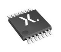
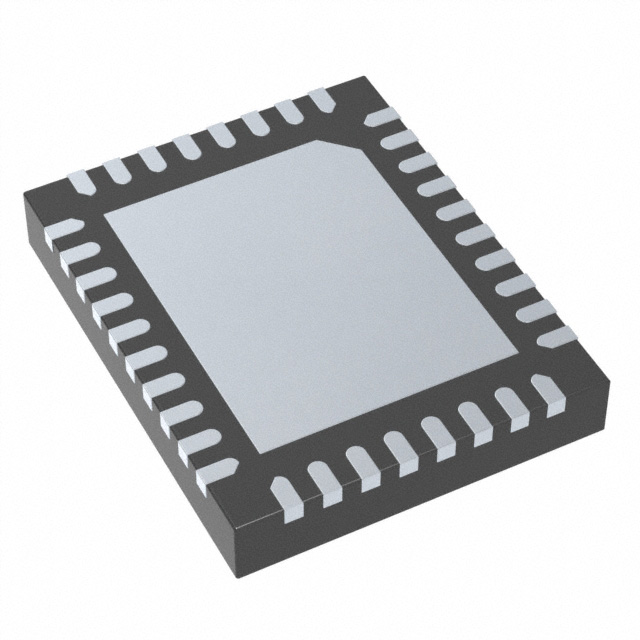
12 Bit 0.65mm Tin ADC AD9226 5V 28-SSOP (0.209, 5.30mm Width)
Unit Price: $98.872685
Ext Price: $98.87


12 Bit 0.65mm Tin ADC AD9226 5V 28-SSOP (0.209, 5.30mm Width)
Master high-speed sampling with the AD9226 12-bit 65 MSPS ADC from Analog Devices. Explore specs, pinouts, and design tips for SDR and FPGA projects. Buy today!
- Executive Summary: What is the AD9226?
- 1. Technical Specifications & Performance Analysis
- 2. Pinout, Package, and Configuration
- 3. Design & Integration Guide (For Engineers & Makers)
- 4. Typical Applications & Use Cases
- 5. Alternatives and Cross-Reference Guide
- 6. Frequently Asked Questions (FAQ)
- 7. Resources
- Specifications
- Datasheet PDF
Executive Summary: What is the AD9226?
The AD9226 is a monolithic, single-supply, 12-bit, 65 MSPS analog-to-digital converter (ADC) designed for high-performance signal processing in communications and imaging systems. It integrates a high-performance sample-and-hold amplifier (SHA) and a programmable voltage reference to provide a complete high-speed data acquisition solution.
Market Position: A high-performance, industry-standard ADC widely used in legacy and modern mid-range high-speed applications.
Top Features: 65 MSPS sampling rate, 12-bit resolution, and low power consumption of only 475 mW.
Primary Audience: Ideal for FPGA developers, SDR (Software Defined Radio) designers, and engineers building high-speed medical imaging or communication equipment.
Supply Status: Active; widely available through major distributors like Analog Devices and global electronics partners.

1. Technical Specifications & Performance Analysis
The AD9226 stands out by balancing speed and power efficiency, making it a staple for systems where thermal management and data throughput are equally critical.
1.1 Core Architecture (Pipeline ADC)
The AD9226 utilizes a multi-stage differential pipelined architecture with digital error correction logic. This architecture ensures that the device maintains 12-bit accuracy even at the maximum 65 MSPS sampling rate. The inclusion of an on-chip Clock Duty Cycle Stabilizer is a major advantage, as it allows the ADC to maintain performance even when the input clock pulse width varies.
1.2 Key Electrical Characteristics
Engineers must pay close attention to the power requirements to ensure signal integrity:
- Supply Voltage: Operates on a single 5 V rail (range: 4.75 V to 5.25 V).
- Power Dissipation: Approximately 475 mW, which is relatively low for a 65 MSPS converter, reducing the need for aggressive active cooling.
- Input Range: Flexible input logic allows for single-ended or differential signals, though differential is preferred for maximum dynamic range.
1.3 Interfaces and Connectivity
The AD9226 features a Parallel Data Interface. This provides a direct, low-latency connection to FPGAs (like Xilinx Artix or Intel Cyclone) and high-speed Digital Signal Processors (DSPs). It also includes an Out-of-Range (OTR) indicator bit, which provides an immediate logic signal if the input voltage exceeds the ADC's range, preventing data clipping errors in software.
2. Pinout, Package, and Configuration
Understanding the physical layout is crucial for PCB routing, especially given the high-frequency nature of the 65 MSPS clock.
2.1 Pin Configuration Guide

VINA/VINB: Differential analog inputs.
CLK: The master sampling clock input.
D0–D11: The 12-bit parallel digital output bus.
OTR: Out-of-Range indicator.
VREF: Internal/External voltage reference pin.
AVDD/DVDD: Separate pins for Analog and Digital power to minimize noise coupling.
2.2 Naming Convention & Ordering Codes
The AD9226 is typically available in suffixes that denote temperature range and package type.
For example:
- AD9226ARS: Standard 28-lead SSOP package.
- AD9226AST: 48-lead LQFP package (often preferred for better thermal dissipation).
- Z-Suffix: Indicates Lead-Free (RoHS compliant) parts.
2.3 Available Packages
| Package Type | Dimensions | Common Use Case |
|---|---|---|
| SSOP-28 | 10.2mm x 5.3mm | Compact consumer electronics |
| LQFP-48 | 7mm x 7mm | Industrial and high-reliability systems |
3. Design & Integration Guide (For Engineers & Makers)
Pro Tip: When working with 65 MSPS, your PCB layout is as important as the chip itself. Use a solid ground plane and keep digital traces away from analog inputs.
3.1 Hardware Implementation
Bypass Capacitors: Place 0.1 µF ceramic capacitors as close as possible to every VDD pin to filter high-frequency switching noise.
PCB Layout: Use a "Star Ground" or a unified ground plane. Avoid splitting ground planes under the ADC unless you are an expert in EMI/EMC, as this can create return loop issues.
Clock Quality: Use a crystal oscillator with low jitter. Avoid using a standard GPIO pin from a microcontroller to drive the CLK pin.
3.2 Common Design Challenges
Issue: Signal Attenuation. The AD9226 often presents a 50-ohm impedance in module forms. If your source is weak, the voltage will drop.
Fix: Use a high-speed buffer amplifier (like the AD8138) to drive the ADC inputs.
Issue: Clock Jitter in SDR. Using an FPGA's internal PLL to generate the ADC clock can introduce jitter, ruining the Signal-to-Noise Ratio (SNR).
Fix: Use a dedicated external low-jitter clock source for sensitive RF applications.
4. Typical Applications & Use Cases
Watch Tutorial: AD9226
4.1 Real-World Example: Software Defined Radio (SDR)
In an SDR application, the AD9226 acts as the bridge between the analog RF front-end and the digital processing core. By sampling at 65 MSPS, it allows for wideband signal capture. The 12-bit resolution provides enough dynamic range to distinguish weak signals from background noise, making it a favorite for amateur radio enthusiasts and communication researchers using FPGA development boards.
5. Alternatives and Cross-Reference Guide
If the AD9226 is out of stock or does not meet your specific resolution needs, consider these alternatives:
Direct Upgrade: AD9244. It is a 14-bit, 65 MSPS ADC that is largely pin-compatible, offering higher precision for the same footprint.
Lower Speed/Cost: AD9220 (10 MSPS) or AD9224 (40 MSPS) for projects where 65 MSPS is overkill.
Competitor Cross: Texas Instruments AFE7222. While not pin-compatible, it offers similar sampling capabilities for integrated analog front-ends.
6. Frequently Asked Questions (FAQ)
Q: What is the difference between AD9226 and AD9244?
A: The AD9226 is 12-bit, while the AD9244 is 14-bit. The AD9244 provides better dynamic range but may be more expensive.
Q: Can the AD9226 be used with an Arduino?
A: No. Standard Arduinos (Uno/Mega) are too slow to handle 65 MSPS data. You need an FPGA or a high-performance MCU with a Parallel Camera Interface (DCMI) or DMA support.
Q: Is the AD9226 suitable for battery-operated devices?
A: Yes, its 475 mW power consumption is efficient for its speed class, though it requires a stable 5V supply which may require a boost converter in 3.7V Li-ion systems.
Q: Does it require an external reference?
A: No, it has an on-board programmable reference, but you can override it with an external reference for higher precision.
7. Resources
Datasheet: Visit the Analog Devices website for the official AD9226 PDF.
Development Tools: Look for "AD9226 ADC Modules" for easy breadboarding with FPGA kits.
Libraries: GitHub contains various Verilog/VHDL modules for interfacing AD9226 with Xilinx and Altera FPGAs.
Specifications
Datasheet PDF
- Datasheets :
- ConflictMineralStatement :
 74HC10 Triple 3-input NAND Gate: Pinout, Equivalent and Datasheet
17 November 20214542
 BC556 PNP Transistor: Pinout, Datasheet, and Equivalent
13 August 20215672
 ATMEGA1284P Microcontroller: Pinout, Datasheet, ATMEGA1284 vs. ATMEGA1284P
18 November 20214641
 STUSB4500 USB PD Controller: Pinout, Features and Datasheet
06 January 20229960
 Exploring the Microchip PIC24F08KL301ESO Microcontroller: A Holistic Analysis
29 February 2024139
 A Comprehensive Guide to LTC7852EUFD-1#PBF DC-DC Switching Controller
06 March 2024143
 LM317M Voltage Regulator: Pinout, Equivalent and Circuits
23 November 20212545
 A Comprehensive Guide to LTC6801HG#3ZZTRPBF Battery Management PMIC
06 March 2024146
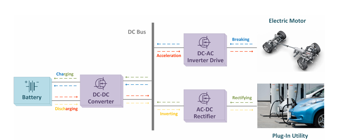 A Hybrid SiC and GaN-Based DC-DC Converter for EVs
20 September 20242437
 What is Comparator?
11 April 20226141
 How to Pick the Perfect Boost Converter for Your Needs
07 June 20251003
 Solar Inverter: Definition, Types and Costs
01 February 20215606
 An Introduction to DIACs
21 May 20254501
 How to Choose MOSFET for Switching Power Supply?
02 March 20228463
 Electronic Components Distributor Utmel to Showcase at 2024 IPC APEX EXPO
10 April 20245480
 Real-time Cloud Analytics in Semiconductor Manufacturing
01 November 20222608
Analog Devices Inc.
In Stock: 155
Minimum: 1 Multiples: 1
Qty
Unit Price
Ext Price
1
$98.872685
$98.87
10
$93.276118
$932.76
100
$87.996338
$8,799.63
500
$83.015413
$41,507.71
1000
$78.316427
$78,316.43
Not the price you want? Send RFQ Now and we'll contact you ASAP.
Inquire for More Quantity
![ADV7513BSWZ]() ADV7513BSWZ
ADV7513BSWZAnalog Devices, Inc.
![AD9877ABSZ]() AD9877ABSZ
AD9877ABSZAnalog Devices, Inc.
![LTC2245CUH#TRPBF]() LTC2245CUH#TRPBF
LTC2245CUH#TRPBFLinear Technology/Analog Devices
![AD7791BRMZ-REEL]() AD7791BRMZ-REEL
AD7791BRMZ-REELAnalog Devices Inc.
![AD7799BRUZ-REEL]() AD7799BRUZ-REEL
AD7799BRUZ-REELAnalog Devices Inc.
![AD7190BRUZ-REEL]() AD7190BRUZ-REEL
AD7190BRUZ-REELAnalog Devices Inc.
![AD7705BRZ-REEL]() AD7705BRZ-REEL
AD7705BRZ-REELAnalog Devices Inc.
![AD7175-2BRUZ-RL7]() AD7175-2BRUZ-RL7
AD7175-2BRUZ-RL7Analog Devices Inc.
![AD7192BRUZ-REEL]() AD7192BRUZ-REEL
AD7192BRUZ-REELAnalog Devices Inc.
![AD9283BRSZ-RL100]() AD9283BRSZ-RL100
AD9283BRSZ-RL100Analog Devices Inc.


