

 Product
 Brand
Brand Articles
 Tools
Tools
HEF4094BT Shift Register: Pinout, Datasheet, Functional Diagram


8 Bit Shift Register 16 Pin 5V SOIC
The HEF4094BT is an 8-stage serial shift register. This article will unlock its pinout, datasheet, application and functional diagram about HEF4094BT.

4094 shift register
HEF4094BT Pinout
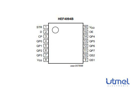
HEF4094BT Pinout
HEF4094BT CAD Model
Symbol
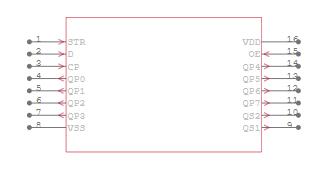
HEF4094BT Symbol
Footprint
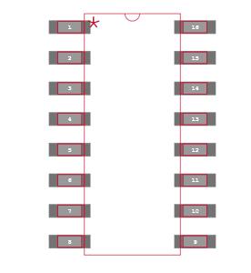
HEF4094BT Footprint
3D Model
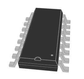
HEF4094BT 3D Model
HEF4094BT Description
The HEF4094BT is an 8 -stage serial shift register. It has a storage latch associated with each stage for strobing data from the serial input to parallel buffered 3-state outputs QP0 to QP7. The parallel outputs may be connected directly to common bus lines. Data is shifted on positive-going clock transitions. The data in each shift register stage is transferred to the storage register when the strobe (STR) input is HIGH. Data in the storage register appears at the outputs whenever the output-enable (OE) signal is HIGH.
It operates over a recommended VDD power supply range of 3 V to 15 V referenced to VSS (usually ground). Unused inputs must be connected to VDD, VSS, or another input.
HEF4094BT Feature
Fully static operation
5 V, 10 V, and 15 V parametric ratings
Standardized symmetrical output characteristics
Specified from -40 ℃ to +85 ℃ and -40 ℃ to +125 ℃
Complies with JEDEC standard JESD 13-B
HEF4094BT Application
Some examples of applications for the HEF4094B are:
• Serial-to-parallel data conversion
• Remote control holding register
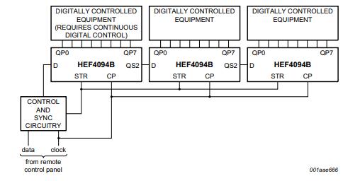
HEF4094BT-Remote control holding register
HEF4094BT Functional Diagram
The following figure shows the functional diagram of HEF4094BT below.
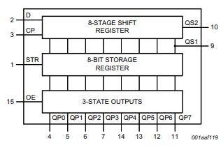
HEF4094BT Functional Diagram
HEF4094BT Logic Diagram
The following figure shows the logic diagram of HEF4094BT below.

HEF4094BT Logic Diagram
Specifications
- TypeParameter
- Package / Case
refers to the protective housing that encases an electronic component, providing mechanical support, electrical connections, and thermal management.
SOIC - Surface Mount
having leads that are designed to be soldered on the side of a circuit board that the body of the component is mounted on.
YES - Number of Pins16
- Number of Elements1
- Published2013
- JESD-609 Code
The "JESD-609 Code" in electronic components refers to a standardized marking code that indicates the lead-free solder composition and finish of electronic components for compliance with environmental regulations.
e4 - Part Status
Parts can have many statuses as they progress through the configuration, analysis, review, and approval stages.
Active - Moisture Sensitivity Level (MSL)
Moisture Sensitivity Level (MSL) is a standardized rating that indicates the susceptibility of electronic components, particularly semiconductors, to moisture-induced damage during storage and the soldering process, defining the allowable exposure time to ambient conditions before they require special handling or baking to prevent failures
1 (Unlimited) - Number of Terminations16
- Terminal Finish
Terminal Finish refers to the surface treatment applied to the terminals or leads of electronic components to enhance their performance and longevity. It can improve solderability, corrosion resistance, and overall reliability of the connection in electronic assemblies. Common finishes include nickel, gold, and tin, each possessing distinct properties suitable for various applications. The choice of terminal finish can significantly impact the durability and effectiveness of electronic devices.
Nickel/Palladium/Gold (Ni/Pd/Au) - Max Operating Temperature
The Maximum Operating Temperature is the maximum body temperature at which the thermistor is designed to operate for extended periods of time with acceptable stability of its electrical characteristics.
70°C - Min Operating Temperature
The "Min Operating Temperature" parameter in electronic components refers to the lowest temperature at which the component is designed to operate effectively and reliably. This parameter is crucial for ensuring the proper functioning and longevity of the component, as operating below this temperature may lead to performance issues or even damage. Manufacturers specify the minimum operating temperature to provide guidance to users on the environmental conditions in which the component can safely operate. It is important to adhere to this parameter to prevent malfunctions and ensure the overall reliability of the electronic system.
-40°C - Additional Feature
Any Feature, including a modified Existing Feature, that is not an Existing Feature.
PARALLEL OUTPUT IS LATCHED; UNLATCHED SERIAL SHIFT RIGHT OUTPUT - Terminal Position
In electronic components, the term "Terminal Position" refers to the physical location of the connection points on the component where external electrical connections can be made. These connection points, known as terminals, are typically used to attach wires, leads, or other components to the main body of the electronic component. The terminal position is important for ensuring proper connectivity and functionality of the component within a circuit. It is often specified in technical datasheets or component specifications to help designers and engineers understand how to properly integrate the component into their circuit designs.
DUAL - Terminal Form
Occurring at or forming the end of a series, succession, or the like; closing; concluding.
GULL WING - Peak Reflow Temperature (Cel)
Peak Reflow Temperature (Cel) is a parameter that specifies the maximum temperature at which an electronic component can be exposed during the reflow soldering process. Reflow soldering is a common method used to attach electronic components to a circuit board. The Peak Reflow Temperature is crucial because it ensures that the component is not damaged or degraded during the soldering process. Exceeding the specified Peak Reflow Temperature can lead to issues such as component failure, reduced performance, or even permanent damage to the component. It is important for manufacturers and assemblers to adhere to the recommended Peak Reflow Temperature to ensure the reliability and functionality of the electronic components.
260 - Number of Functions1
- Supply Voltage
Supply voltage refers to the electrical potential difference provided to an electronic component or circuit. It is crucial for the proper operation of devices, as it powers their functions and determines performance characteristics. The supply voltage must be within specified limits to ensure reliability and prevent damage to components. Different electronic devices have specific supply voltage requirements, which can vary widely depending on their design and intended application.
5V - Frequency
In electronic components, the parameter "Frequency" refers to the rate at which a signal oscillates or cycles within a given period of time. It is typically measured in Hertz (Hz) and represents how many times a signal completes a full cycle in one second. Frequency is a crucial aspect in electronic components as it determines the behavior and performance of various devices such as oscillators, filters, and communication systems. Understanding the frequency characteristics of components is essential for designing and analyzing electronic circuits to ensure proper functionality and compatibility with other components in a system.
28MHz - Time@Peak Reflow Temperature-Max (s)
Time@Peak Reflow Temperature-Max (s) refers to the maximum duration that an electronic component can be exposed to the peak reflow temperature during the soldering process, which is crucial for ensuring reliable solder joint formation without damaging the component.
30 - Temperature Grade
Temperature grades represent a tire's resistance to heat and its ability to dissipate heat when tested under controlled laboratory test conditions.
AUTOMOTIVE - Voltage
Voltage is a measure of the electric potential difference between two points in an electrical circuit. It is typically represented by the symbol "V" and is measured in volts. Voltage is a crucial parameter in electronic components as it determines the flow of electric current through a circuit. It is responsible for driving the movement of electrons from one point to another, providing the energy needed for electronic devices to function properly. In summary, voltage is a fundamental concept in electronics that plays a key role in the operation and performance of electronic components.
15V - Max Supply Voltage
In general, the absolute maximum common-mode voltage is VEE-0.3V and VCC+0.3V, but for products without a protection element at the VCC side, voltages up to the absolute maximum rated supply voltage (i.e. VEE+36V) can be supplied, regardless of supply voltage.
15.5V - Min Supply Voltage
The minimum supply voltage (V min ) is explored for sequential logic circuits by statistically simulating the impact of within-die process variations and gate-dielectric soft breakdown on data retention and hold time.
4.5V - Number of Bits8
- Logic Function
In electronic components, the term "Logic Function" refers to the specific operation or behavior of a component based on its input signals. It describes how the component processes the input signals to produce the desired output. Logic functions are fundamental to digital circuits and are used to perform logical operations such as AND, OR, NOT, and XOR.Each electronic component, such as logic gates or flip-flops, is designed to perform a specific logic function based on its internal circuitry. By understanding the logic function of a component, engineers can design and analyze complex digital systems to ensure proper functionality and performance. Different logic functions can be combined to create more complex operations, allowing for the creation of sophisticated digital devices and systems.
Shift Register - Output Characteristics
Output characteristics in electronic components refer to the relationship between the output voltage and output current across a range of input conditions. This parameter is essential for understanding how a device, such as a transistor or operational amplifier, behaves under various loads and operating points. It provides insights into the efficiency, performance, and limitations of the component, helping designers to make informed choices for circuits and applications.
3-STATE - Output Polarity
Output polarity in electronic components refers to the orientation of the output signal in relation to the ground or reference voltage. It indicates whether the output voltage is positive or negative with respect to the ground. Positive output polarity means the signal is higher than the ground potential, while negative output polarity signifies that the signal is lower than the ground. This characteristic is crucial for determining compatibility with other components in a circuit and ensuring proper signal processing.
TRUE - Logic IC Type
Logic IC Type refers to the type of integrated circuit (IC) that is specifically designed to perform logical operations. These ICs are commonly used in digital electronic devices to process and manipulate binary data according to predefined logic functions. The Logic IC Type parameter typically specifies the specific logic family or technology used in the IC, such as TTL (Transistor-Transistor Logic), CMOS (Complementary Metal-Oxide-Semiconductor), or ECL (Emitter-Coupled Logic). Understanding the Logic IC Type is important for selecting the appropriate IC for a given application, as different logic families have varying characteristics in terms of speed, power consumption, and noise immunity.
SERIAL IN PARALLEL OUT - Trigger Type
Trigger Type in electronic components refers to the mechanism or method by which a device, such as a flip-flop or timer, responds to an input signal. It defines how the device transitions between states based on specific conditions, such as rising or falling edges of a signal, levels, or pulses. Different trigger types such as edge-triggered, level-triggered, or pulse-triggered influence the timing and behavior of the circuit, thereby determining how input signals affect the output in various applications.
POSITIVE EDGE - Propagation Delay (tpd)
Propagation delay (tpd) is a crucial parameter in electronic components, especially in digital circuits. It refers to the time taken for a signal to travel from the input of a component to its output. This delay is caused by various factors such as the internal circuitry, interconnections, and the physical properties of the component. Propagation delay is essential to consider in designing circuits to ensure proper timing and functionality. It is typically measured in nanoseconds or picoseconds and plays a significant role in determining the overall performance and speed of electronic systems.
330 ns - Count Direction
Count Direction in electronic components refers to the direction in which a counter or digital circuit increments or decrements its count. It indicates whether the counting process moves forward (upward count) or backward (downward count). This parameter is crucial in applications such as timers, event counters, and digital clocks, where precise control over the counting sequence is necessary. The count direction can usually be set or controlled through external inputs, allowing for flexibility in circuit operation.
RIGHT - Length9.9mm
- Width3.9mm
- REACH SVHC
The parameter "REACH SVHC" in electronic components refers to the compliance with the Registration, Evaluation, Authorization, and Restriction of Chemicals (REACH) regulation regarding Substances of Very High Concern (SVHC). SVHCs are substances that may have serious effects on human health or the environment, and their use is regulated under REACH to ensure their safe handling and minimize their impact.Manufacturers of electronic components need to declare if their products contain any SVHCs above a certain threshold concentration and provide information on the safe use of these substances. This information allows customers to make informed decisions about the potential risks associated with using the components and take appropriate measures to mitigate any hazards.Ensuring compliance with REACH SVHC requirements is essential for electronics manufacturers to meet regulatory standards, protect human health and the environment, and maintain transparency in their supply chain. It also demonstrates a commitment to sustainability and responsible manufacturing practices in the electronics industry.
No SVHC - RoHS Status
RoHS means “Restriction of Certain Hazardous Substances” in the “Hazardous Substances Directive” in electrical and electronic equipment.
RoHS Compliant
HEF4094BT Package
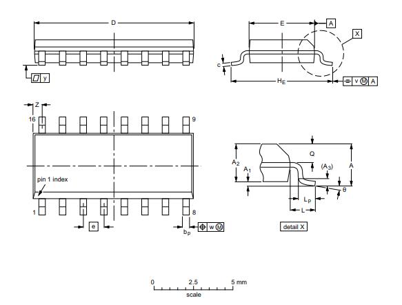
HEF4094BT Package
HEF4094BT Manufacturer
Nexperia is a dedicated global leader in Discretes, Logic and MOSFETs devices. This new company became independent at the beginning of 2017. Focused on efficiency, Nexperia produces consistently reliable semiconductor components at a high volume: 85 billion annually. The company’s extensive portfolio meets the stringent standards set by the Automotive industry. And industry-leading small packages, produced in their own manufacturing facilities, combine power and thermal efficiency with best-in-class quality levels. Built on over half a century of expertise, Nexperia has 11,000 employees across Asia, Europe and the U.S. supporting customers globally.
The more similar parts come from Nexperia following
HEF4094B
HEF4094BT,652 and so on
Datasheet PDF
- Datasheets :
- RohsStatement :
The HEF4094BT has a storage latch associated with each stage for what?
Strobing data from the serial input to parallel buffered 3-state outputs QP0 to QP7.
What may be connected directly to common bus lines?
Parallel outputs.
When is data shifted?
Positive-going clock transitions
What does the HEF4094BT operate over?
VDD power supply range of 3 V to 15 V.
What is a shift registor?
A shift register is a type of digital circuit using a cascade of flip-flops where the output of one flip-flop is connected to the input of the next. They share a single clock signal, which causes the data stored in the system to shift from one location to the next.
What is the use of shift registers?
Shift Registers are used for data storage or for the movement of data and are therefore commonly used inside calculators or computers to store data such as two binary numbers before they are added together, or to convert the data from either a serial to parallel or parallel to serial format.
 BC817-40 NPN Transistor: Pinout, Equivalent and Datasheet
26 March 20226251
 M95020-W EEPROM: Pinout, Features and Datasheet
07 January 20222291
 Microchip PIC16LF1516ISP: A Comprehensive Overview of Features and Applications
29 February 2024287
 P6KE33A TVS Diodes: System, Pinout, and Datasheet
20 April 20222618
 How to Interface Stepper Motor with PIC16F877A Microcontroller?
01 April 20223839
 AD9834 DDS Device: Pinout, Datasheet and Alternatives
02 September 20214113
 A Comprehensive Guide to LTC6652AHMS8-3#TRPBF Voltage Reference IC
06 March 2024197
 PCA9306DCUR Translator: Features, Applications and Datasheet
09 November 20231755
 Top 10 Popular Semiconductor Companies in 2026
13 August 202617100
 TinyML Takes a Major Step Forward as Israeli Company Releases New Chip
19 April 20221181
 What is an Optical Sensor?
19 March 20217234
 Role of Real-Time Clocks in Modern Electronics
08 July 20242871
 What is a Knock Sensor?
08 January 202620403
 A Beginner's Guide to the 2N5551 Transistor and Its Uses
27 May 20256244
 What is an Instrumentation Amplifier?
27 March 202513605
 What Size Wire for a 60 Amp Breaker? The Complete NEC Guide
22 May 20264105
Nexperia
In Stock: 40000
United States
China
Canada
Japan
Russia
Germany
United Kingdom
Singapore
Italy
Hong Kong(China)
Taiwan(China)
France
Korea
Mexico
Netherlands
Malaysia
Austria
Spain
Switzerland
Poland
Thailand
Vietnam
India
United Arab Emirates
Afghanistan
Åland Islands
Albania
Algeria
American Samoa
Andorra
Angola
Anguilla
Antigua & Barbuda
Argentina
Armenia
Aruba
Australia
Azerbaijan
Bahamas
Bahrain
Bangladesh
Barbados
Belarus
Belgium
Belize
Benin
Bermuda
Bhutan
Bolivia
Bonaire, Sint Eustatius and Saba
Bosnia & Herzegovina
Botswana
Brazil
British Indian Ocean Territory
British Virgin Islands
Brunei
Bulgaria
Burkina Faso
Burundi
Cabo Verde
Cambodia
Cameroon
Cayman Islands
Central African Republic
Chad
Chile
Christmas Island
Cocos (Keeling) Islands
Colombia
Comoros
Congo
Congo (DRC)
Cook Islands
Costa Rica
Côte d’Ivoire
Croatia
Cuba
Curaçao
Cyprus
Czechia
Denmark
Djibouti
Dominica
Dominican Republic
Ecuador
Egypt
El Salvador
Equatorial Guinea
Eritrea
Estonia
Eswatini
Ethiopia
Falkland Islands
Faroe Islands
Fiji
Finland
French Guiana
French Polynesia
Gabon
Gambia
Georgia
Ghana
Gibraltar
Greece
Greenland
Grenada
Guadeloupe
Guam
Guatemala
Guernsey
Guinea
Guinea-Bissau
Guyana
Haiti
Honduras
Hungary
Iceland
Indonesia
Iran
Iraq
Ireland
Isle of Man
Israel
Jamaica
Jersey
Jordan
Kazakhstan
Kenya
Kiribati
Kosovo
Kuwait
Kyrgyzstan
Laos
Latvia
Lebanon
Lesotho
Liberia
Libya
Liechtenstein
Lithuania
Luxembourg
Macao(China)
Madagascar
Malawi
Maldives
Mali
Malta
Marshall Islands
Martinique
Mauritania
Mauritius
Mayotte
Micronesia
Moldova
Monaco
Mongolia
Montenegro
Montserrat
Morocco
Mozambique
Myanmar
Namibia
Nauru
Nepal
New Caledonia
New Zealand
Nicaragua
Niger
Nigeria
Niue
Norfolk Island
North Korea
North Macedonia
Northern Mariana Islands
Norway
Oman
Pakistan
Palau
Palestinian Authority
Panama
Papua New Guinea
Paraguay
Peru
Philippines
Pitcairn Islands
Portugal
Puerto Rico
Qatar
Réunion
Romania
Rwanda
Samoa
San Marino
São Tomé & Príncipe
Saudi Arabia
Senegal
Serbia
Seychelles
Sierra Leone
Sint Maarten
Slovakia
Slovenia
Solomon Islands
Somalia
South Africa
South Sudan
Sri Lanka
St Helena, Ascension, Tristan da Cunha
St. Barthélemy
St. Kitts & Nevis
St. Lucia
St. Martin
St. Pierre & Miquelon
St. Vincent & Grenadines
Sudan
Suriname
Svalbard & Jan Mayen
Sweden
Syria
Tajikistan
Tanzania
Timor-Leste
Togo
Tokelau
Tonga
Trinidad & Tobago
Tunisia
Turkey
Turkmenistan
Turks & Caicos Islands
Tuvalu
U.S. Outlying Islands
U.S. Virgin Islands
Uganda
Ukraine
Uruguay
Uzbekistan
Vanuatu
Vatican City
Venezuela
Wallis & Futuna
Yemen
Zambia
Zimbabwe
![74HC595D,118]() 74HC595D,118
74HC595D,118Nexperia USA Inc.
![74HC164D,653]() 74HC164D,653
74HC164D,653Nexperia USA Inc.
![74HC164PW,118]() 74HC164PW,118
74HC164PW,118Nexperia USA Inc.
![74HC4094D,653]() 74HC4094D,653
74HC4094D,653Nexperia USA Inc.
![HEF4021BT,653]() HEF4021BT,653
HEF4021BT,653Nexperia USA Inc.
![74AHC595PW,118]() 74AHC595PW,118
74AHC595PW,118Nexperia USA Inc.
![74AHC595D,118]() 74AHC595D,118
74AHC595D,118Nexperia USA Inc.
![NPIC6C596ADJ]() NPIC6C596ADJ
NPIC6C596ADJNexperia USA Inc.
![NPIC6C595D-Q100,11]() NPIC6C595D-Q100,11
NPIC6C595D-Q100,11Nexperia USA Inc.
![74HCT164D,653]() 74HCT164D,653
74HCT164D,653Nexperia USA Inc.


