
 Product
 Brand
Brand Articles
 Tools
Tools
INA128 Amplifier: Pinout, Equivalent and Datasheet

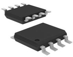
15mA per Channel 2nA 110 dB Instrumentational OP Amps 0.005μA 4.5V~36V ±2.25V~18V INA128 8 Pins 8-SOIC (0.154, 3.90mm Width)


15mA per Channel 2nA 110 dB Instrumentational OP Amps 0.005μA 4.5V~36V ±2.25V~18V INA128 8 Pins 8-SOIC (0.154, 3.90mm Width)
The INA128 is low power, general purpose instrumentation amplifier offering excellent accuracy. Furthermore, Huge range of Semiconductors, Capacitors, Resistors and IcS in stock. Welcome RFQ.

Instrumentation Amplifiers
INA128 Pinout

Pinout
INA128 CAD Model

symbol

footprint

3D Model
INA128 Overview
The INA128 is low power, general purpose instrumentation amplifier offering excellent accuracy. The versatile 3-op amp design and small size make them ideal for a wide range of applications. Current-feedback input circuitry provides wide bandwidth even at high gain (200kHz at G = 100). A single external resistor sets any gain from 1 to 10,000. The INA128 provides an industry-standard gain equation. The INA128 is laser trimmed for very low offset voltage (50µV), drift (0.5µV/°C) and high common-mode rejection (120dB at G ≥ 100). It operates with power supplies as low as ±2.25V, and quiescent current is only 700µA—ideal for battery-operated systems. Internal input protection can withstand up to ±40V without damage. The INA128 is available in 8-pin plastic DIP and SO-8 surface-mount packages, specified for the –40°C to +85°C temperature range. The INA128 is also available in a dual configuration, the INA2128.
This article provides you with a basic overview of the INA128, including its pin descriptions, features and specifications, etc., to help you quickly understand what INA128 is.
INA128 Features
● Low Offset Voltage: 50µV max
● Low Drift: 0.5µV/℃ max
● Low Input Bias Current: 5nA max
● High CMR: 120dB min
● Inputs Protected to ±40V
● Wide Supply Range: ±2.25V to ±18V
● Low Quiescent Current: 700µA
● 8-PIN Plastic DIP, SO-8
Specifications
- TypeParameter
- Lifecycle Status
Lifecycle Status refers to the current stage of an electronic component in its product life cycle, indicating whether it is active, obsolete, or transitioning between these states. An active status means the component is in production and available for purchase. An obsolete status indicates that the component is no longer being manufactured or supported, and manufacturers typically provide a limited time frame for support. Understanding the lifecycle status is crucial for design engineers to ensure continuity and reliability in their projects.
ACTIVE (Last Updated: 3 days ago) - Factory Lead Time6 Weeks
- Contact Plating
Contact plating (finish) provides corrosion protection for base metals and optimizes the mechanical and electrical properties of the contact interfaces.
Gold - Mounting Type
The "Mounting Type" in electronic components refers to the method used to attach or connect a component to a circuit board or other substrate, such as through-hole, surface-mount, or panel mount.
Surface Mount - Package / Case
refers to the protective housing that encases an electronic component, providing mechanical support, electrical connections, and thermal management.
8-SOIC (0.154, 3.90mm Width) - Surface Mount
having leads that are designed to be soldered on the side of a circuit board that the body of the component is mounted on.
YES - Number of Pins8
- Weight75.891673mg
- Operating Temperature
The operating temperature is the range of ambient temperature within which a power supply, or any other electrical equipment, operate in. This ranges from a minimum operating temperature, to a peak or maximum operating temperature, outside which, the power supply may fail.
-40°C~125°C - Packaging
Semiconductor package is a carrier / shell used to contain and cover one or more semiconductor components or integrated circuits. The material of the shell can be metal, plastic, glass or ceramic.
Tube - JESD-609 Code
The "JESD-609 Code" in electronic components refers to a standardized marking code that indicates the lead-free solder composition and finish of electronic components for compliance with environmental regulations.
e4 - Pbfree Code
The "Pbfree Code" parameter in electronic components refers to the code or marking used to indicate that the component is lead-free. Lead (Pb) is a toxic substance that has been widely used in electronic components for many years, but due to environmental concerns, there has been a shift towards lead-free alternatives. The Pbfree Code helps manufacturers and users easily identify components that do not contain lead, ensuring compliance with regulations and promoting environmentally friendly practices. It is important to pay attention to the Pbfree Code when selecting electronic components to ensure they meet the necessary requirements for lead-free applications.
yes - Part Status
Parts can have many statuses as they progress through the configuration, analysis, review, and approval stages.
Active - Moisture Sensitivity Level (MSL)
Moisture Sensitivity Level (MSL) is a standardized rating that indicates the susceptibility of electronic components, particularly semiconductors, to moisture-induced damage during storage and the soldering process, defining the allowable exposure time to ambient conditions before they require special handling or baking to prevent failures
3 (168 Hours) - ECCN Code
An ECCN (Export Control Classification Number) is an alphanumeric code used by the U.S. Bureau of Industry and Security to identify and categorize electronic components and other dual-use items that may require an export license based on their technical characteristics and potential for military use.
EAR99 - Resistance
Resistance is a fundamental property of electronic components that measures their opposition to the flow of electric current. It is denoted by the symbol "R" and is measured in ohms (Ω). Resistance is caused by the collisions of electrons with atoms in a material, which generates heat and reduces the flow of current. Components with higher resistance will impede the flow of current more than those with lower resistance. Resistance plays a crucial role in determining the behavior and functionality of electronic circuits, such as limiting current flow, voltage division, and controlling power dissipation.
100GOhm - Terminal Position
In electronic components, the term "Terminal Position" refers to the physical location of the connection points on the component where external electrical connections can be made. These connection points, known as terminals, are typically used to attach wires, leads, or other components to the main body of the electronic component. The terminal position is important for ensuring proper connectivity and functionality of the component within a circuit. It is often specified in technical datasheets or component specifications to help designers and engineers understand how to properly integrate the component into their circuit designs.
DUAL - Terminal Form
Occurring at or forming the end of a series, succession, or the like; closing; concluding.
GULL WING - Peak Reflow Temperature (Cel)
Peak Reflow Temperature (Cel) is a parameter that specifies the maximum temperature at which an electronic component can be exposed during the reflow soldering process. Reflow soldering is a common method used to attach electronic components to a circuit board. The Peak Reflow Temperature is crucial because it ensures that the component is not damaged or degraded during the soldering process. Exceeding the specified Peak Reflow Temperature can lead to issues such as component failure, reduced performance, or even permanent damage to the component. It is important for manufacturers and assemblers to adhere to the recommended Peak Reflow Temperature to ensure the reliability and functionality of the electronic components.
260 - Number of Functions1
- Supply Voltage
Supply voltage refers to the electrical potential difference provided to an electronic component or circuit. It is crucial for the proper operation of devices, as it powers their functions and determines performance characteristics. The supply voltage must be within specified limits to ensure reliability and prevent damage to components. Different electronic devices have specific supply voltage requirements, which can vary widely depending on their design and intended application.
15V - Base Part Number
The "Base Part Number" (BPN) in electronic components serves a similar purpose to the "Base Product Number." It refers to the primary identifier for a component that captures the essential characteristics shared by a group of similar components. The BPN provides a fundamental way to reference a family or series of components without specifying all the variations and specific details.
INA128 - Pin Count
a count of all of the component leads (or pins)
8 - Number of Circuits1
- Operating Supply Current
Operating Supply Current, also known as supply current or quiescent current, is a crucial parameter in electronic components that indicates the amount of current required for the device to operate under normal conditions. It represents the current drawn by the component from the power supply while it is functioning. This parameter is important for determining the power consumption of the component and is typically specified in datasheets to help designers calculate the overall power requirements of their circuits. Understanding the operating supply current is essential for ensuring proper functionality and efficiency of electronic systems.
700μA - Nominal Supply Current
Nominal current is the same as the rated current. It is the current drawn by the motor while delivering rated mechanical output at its shaft.
750μA - Quiescent Current
The quiescent current is defined as the current level in the amplifier when it is producing an output of zero.
700μA - Slew Rate
the maximum rate of output voltage change per unit time.
4V/μs - Amplifier Type
Amplifier Type refers to the classification or categorization of amplifiers based on their design, functionality, and characteristics. Amplifiers are electronic devices that increase the amplitude of a signal, such as voltage or current. The type of amplifier determines its specific application, performance capabilities, and operating characteristics. Common types of amplifiers include operational amplifiers (op-amps), power amplifiers, audio amplifiers, and radio frequency (RF) amplifiers. Understanding the amplifier type is crucial for selecting the right component for a particular circuit or system design.
Instrumentation - Common Mode Rejection Ratio
Common Mode Rejection Ratio (CMRR) is a measure of the ability of a differential amplifier to reject input signals that are common to both input terminals. It is defined as the ratio of the differential gain to the common mode gain. A high CMRR indicates that the amplifier can effectively eliminate noise and interference that affects both inputs simultaneously, enhancing the fidelity of the amplified signal. CMRR is typically expressed in decibels (dB), with higher values representing better performance in rejecting common mode signals.
110 dB - Current - Input Bias
The parameter "Current - Input Bias" in electronic components refers to the amount of current required at the input terminal of a device to maintain proper operation. It is a crucial specification as it determines the minimum input current needed for the component to function correctly. Input bias current can affect the performance and accuracy of the device, especially in precision applications where small signal levels are involved. It is typically specified in datasheets for operational amplifiers, transistors, and other semiconductor devices to provide users with important information for circuit design and analysis.
2nA - Voltage - Supply, Single/Dual (±)
The parameter "Voltage - Supply, Single/Dual (±)" in electronic components refers to the power supply voltage required for the proper operation of the component. This parameter indicates whether the component requires a single power supply voltage (e.g., 5V) or a dual power supply voltage (e.g., ±15V). For components that require a single power supply voltage, only one voltage level is needed for operation. On the other hand, components that require a dual power supply voltage need both positive and negative voltage levels to function correctly.Understanding the voltage supply requirements of electronic components is crucial for designing and integrating them into circuits to ensure proper functionality and prevent damage due to incorrect voltage levels.
4.5V~36V ±2.25V~18V - Output Current per Channel
Output Current per Channel is a specification commonly found in electronic components such as amplifiers, audio interfaces, and power supplies. It refers to the maximum amount of electrical current that can be delivered by each individual output channel of the component. This parameter is important because it determines the capacity of the component to drive connected devices or loads. A higher output current per channel means the component can deliver more power to connected devices, while a lower output current may limit the performance or functionality of the component in certain applications. It is crucial to consider the output current per channel when selecting electronic components to ensure they can meet the power requirements of the intended system or setup.
15mA - Input Offset Voltage (Vos)
Input Offset Voltage (Vos) is a key parameter in electronic components, particularly in operational amplifiers. It refers to the voltage difference that must be applied between the two input terminals of the amplifier to nullify the output voltage when the input terminals are shorted together. In simpler terms, it represents the voltage required to bring the output of the amplifier to zero when there is no input signal present. Vos is an important parameter as it can introduce errors in the output signal of the amplifier, especially in precision applications where accuracy is crucial. Minimizing Vos is essential to ensure the amplifier operates with high precision and accuracy.
125μV - Bandwidth
In electronic components, "Bandwidth" refers to the range of frequencies over which the component can effectively operate or pass signals without significant loss or distortion. It is a crucial parameter for devices like amplifiers, filters, and communication systems. The bandwidth is typically defined as the difference between the upper and lower frequencies at which the component's performance meets specified criteria, such as a certain level of signal attenuation or distortion. A wider bandwidth indicates that the component can handle a broader range of frequencies, making it more versatile for various applications. Understanding the bandwidth of electronic components is essential for designing and optimizing circuits to ensure proper signal transmission and reception within the desired frequency range.
1.3MHz - Gain Bandwidth Product
The gain–bandwidth product (designated as GBWP, GBW, GBP, or GB) for an amplifier is the product of the amplifier's bandwidth and the gain at which the bandwidth is measured.
1.3MHz - Neg Supply Voltage-Nom (Vsup)
The parameter "Neg Supply Voltage-Nom (Vsup)" in electronic components refers to the nominal negative supply voltage that the component requires to operate within its specified performance characteristics. This parameter indicates the minimum voltage level that must be provided to the component's negative supply pin for proper functionality. It is important to ensure that the negative supply voltage provided to the component does not exceed the maximum specified value to prevent damage or malfunction. Understanding and adhering to the specified negative supply voltage requirements is crucial for the reliable operation of the electronic component in a circuit.
-15V - Voltage Gain
Voltage gain is a measure of how much an electronic component or circuit amplifies an input voltage signal to produce an output voltage signal. It is typically expressed as a ratio or in decibels (dB). A higher voltage gain indicates a greater amplification of the input signal. Voltage gain is an important parameter in amplifiers, where it determines the level of amplification provided by the circuit. It is calculated by dividing the output voltage by the input voltage and is a key factor in determining the overall performance and functionality of electronic devices.
80dB - Average Bias Current-Max (IIB)
The parameter "Average Bias Current-Max (IIB)" in electronic components refers to the maximum average bias current that the component can handle without exceeding its specified operating limits. Bias current is the current that flows through a component when it is in its quiescent state or when it is not actively processing a signal. Exceeding the maximum average bias current can lead to overheating, reduced performance, or even damage to the component. Therefore, it is important to ensure that the bias current does not exceed the specified maximum value to maintain the reliability and longevity of the electronic component.
0.005μA - Voltage - Input Offset
Voltage - Input Offset is a parameter that refers to the difference in voltage between the input terminals of an electronic component, such as an operational amplifier, when the input voltage is zero. It is an important characteristic that can affect the accuracy and performance of the component in various applications. A low input offset voltage is desirable as it indicates that the component will have minimal error in its output when the input signal is near zero. Manufacturers typically provide this specification in the component's datasheet to help users understand the component's behavior and make informed decisions when designing circuits.
25μV - -3db Bandwidth
The "-3dB bandwidth" of an electronic component refers to the frequency range over which the component's output signal power is reduced by 3 decibels (dB) compared to its maximum output power. This parameter is commonly used to describe the frequency response of components such as amplifiers, filters, and other signal processing devices. The -3dB point is significant because it represents the half-power point, where the output signal power is reduced to half of its maximum value. Understanding the -3dB bandwidth is important for designing and analyzing electronic circuits to ensure that signals are accurately processed within the desired frequency range.
1.3MHz - Dual Supply Voltage
Dual Supply Voltage refers to an electronic component's requirement for two separate power supply voltages, typically one positive and one negative. This configuration is commonly used in operational amplifiers, analog circuits, and certain digital devices to allow for greater signal handling capabilities and improved performance. The use of dual supply voltages enables the device to process bipolar signals, thereby enhancing its functionality in various applications.
15V - Input Voltage Noise Density
Input Voltage Noise Density refers to the measure of noise voltage present at the input of an electronic component, typically expressed in volts per square root hertz (V/√Hz). It characterizes the amount of noise introduced by the component, independent of the signal level. This parameter is crucial for understanding the overall performance of amplifiers, sensors, and other devices, as it impacts the signal-to-noise ratio and limits the achievable resolution and sensitivity in electronic systems. Lower values of input voltage noise density indicate better performance in terms of noise characteristics.
8nV/sqrt Hz - Number of Amplifiers3
- Voltage Gain-Nom
Voltage Gain-Nom is a parameter used to describe the ratio of the output voltage to the input voltage in electronic components such as amplifiers. It represents the amplification factor of the component and indicates how much the input voltage is amplified to produce the output voltage. The "Nom" in the term signifies that this value is the nominal or typical voltage gain under specified operating conditions. A higher voltage gain indicates a greater amplification of the input signal, while a lower voltage gain signifies less amplification. This parameter is crucial in determining the performance and functionality of electronic circuits and devices.
10 - Non-linearity-Max
Non-linearity-Max is a parameter used to describe the maximum level of non-linearity exhibited by an electronic component or system. Non-linearity refers to the deviation of the component's output from a straight line when compared to its input signal. In the context of electronic components, such as amplifiers or sensors, non-linearity can introduce distortion or inaccuracies in the output signal. The "Non-linearity-Max" parameter specifies the maximum amount of deviation allowed before the component is considered to be operating outside of its specified linear range. It is an important characteristic to consider when designing or selecting components for applications where precise and accurate signal processing is required.
0.004% - Height1.75mm
- Length4.9mm
- Width3.91mm
- Thickness
Thickness in electronic components refers to the measurement of how thick a particular material or layer is within the component structure. It can pertain to various aspects, such as the thickness of a substrate, a dielectric layer, or conductive traces. This parameter is crucial as it impacts the electrical, mechanical, and thermal properties of the component, influencing its performance and reliability in electronic circuits.
1.58mm - REACH SVHC
The parameter "REACH SVHC" in electronic components refers to the compliance with the Registration, Evaluation, Authorization, and Restriction of Chemicals (REACH) regulation regarding Substances of Very High Concern (SVHC). SVHCs are substances that may have serious effects on human health or the environment, and their use is regulated under REACH to ensure their safe handling and minimize their impact.Manufacturers of electronic components need to declare if their products contain any SVHCs above a certain threshold concentration and provide information on the safe use of these substances. This information allows customers to make informed decisions about the potential risks associated with using the components and take appropriate measures to mitigate any hazards.Ensuring compliance with REACH SVHC requirements is essential for electronics manufacturers to meet regulatory standards, protect human health and the environment, and maintain transparency in their supply chain. It also demonstrates a commitment to sustainability and responsible manufacturing practices in the electronics industry.
No SVHC - Radiation Hardening
Radiation hardening is the process of making electronic components and circuits resistant to damage or malfunction caused by high levels of ionizing radiation, especially for environments in outer space (especially beyond the low Earth orbit), around nuclear reactors and particle accelerators, or during nuclear accidents or nuclear warfare.
No - RoHS Status
RoHS means “Restriction of Certain Hazardous Substances” in the “Hazardous Substances Directive” in electrical and electronic equipment.
ROHS3 Compliant - Lead Free
Lead Free is a term used to describe electronic components that do not contain lead as part of their composition. Lead is a toxic material that can have harmful effects on human health and the environment, so the electronics industry has been moving towards lead-free components to reduce these risks. Lead-free components are typically made using alternative materials such as silver, copper, and tin. Manufacturers must comply with regulations such as the Restriction of Hazardous Substances (RoHS) directive to ensure that their products are lead-free and environmentally friendly.
Lead Free
INA128 Functional Block Diagram

Basic Connections
INA128 Equivalent
| Model number | Manufacturer | Description |
| LT1101ISW | Analog Devices Inc | Instrumentation Amplifier, 1 Func, 950uV Offset-Max, 0.037MHz Band Width, PDSO16 |
| INA110BG-BI | Texas Instruments | INSTRUMENTATION AMPLIFIER, 3250uV OFFSET-MAX, 2.5MHz BAND WIDTH, CDIP16 |
| INA128UA/2K5 | Burr-Brown Corp | Instrumentation Amplifier, 1 Func, 1125uV Offset-Max, 1.3MHz Band Width, PDSO8, GREEN, PLASTIC, MS-012AA, SOIC-8 |
| LT1101ISW#PBF | Analog Devices Inc | Precision, Micropower, Single Supply Instrumentation Amplifier (Fixed Gain = 10 or 100) |
| AD624BDZ | Rochester Electronics LLC | INSTRUMENTATION AMPLIFIER, 75 uV OFFSET-MAX, 1 MHz BAND WIDTH, CDIP16, CERAMIC, DIP-16 |
| INA114BUE4 | Texas Instruments | INSTRUMENTATION AMPLIFIER, 50uV OFFSET-MAX, 1MHz BAND WIDTH, PDSO16, GREEN, SOIC-16 |
| PGA205BPG4 | Texas Instruments | Programmable Gain Instrumentation Amplifier 16-PDIP -40 to 85 |
| AD524BDZ | Analog Devices Inc | Precision Instrumentation Amplifier |
| INA101KU/1KE4 | Texas Instruments | INSTRUMENTATION AMPLIFIER, 0.3MHz BAND WIDTH, PDSO16, ROHS COMPLIANT, SOIC-16 |
| AD524ARZ-16-REEL7 | Analog Devices Inc | Precision Instrumentation Amplifier |
Parts with Similar Specs
- ImagePart NumberManufacturerPackage / CaseNumber of PinsNumber of CircuitsSlew RateGain Bandwidth ProductInput Offset Voltage (Vos)Common Mode Rejection RatioSupply VoltageView Compare
![INA128UAE4]()
INA128UAE4
8-SOIC (0.154, 3.90mm Width)
8
1
4V/μs
1.3 MHz
125 μV
110 dB
15 V
![INA129UA/2K5]()
8-SOIC (0.154, 3.90mm Width)
8
1
4V/μs
1.3 MHz
25 μV
110 dB
15 V
![INA128UA]()
8-SOIC (0.154, 3.90mm Width)
8
-
4V/μs
1.3 MHz
25 μV
110 dB
15 V
![INA129UA]()
8-SOIC (0.154, 3.90mm Width)
8
-
4V/μs
1.3 MHz
125 μV
110 dB
15 V

INA128 Applications
● Bridge Amplifier
● Thermocouple Amplifier
● RTD Sensor Amplifier
● Medical Instrumentation
● Data Acquisition
INA128 Package

Package
INA128 Manufacturer
Texas Instruments (TI) emerges as a globally recognized semiconductor manufacturer expanded into 35 countries. It has seen a rapid growth. In 1958, TIer firstly introduced the working integrated circuit. And today more than 30,000 TIers worldwide are committed to designing, manufacturing, and selling analog and embedded processing chips. They aspire to solve challenges as well as change the world through their technologies.
Texas Instruments (TI) is an American technology company that designs and manufactures semiconductors and various integrated circuits, which it sells to electronics designers and manufacturers globally. Its headquarters are in Dallas, Texas, United States. TI is one of the top ten semiconductor companies worldwide, based on sales volume.Texas Instruments's focus is on developing analog chips and embedded processors, which accounts for more than 80% of their revenue. TI also produces TI digital light processing (DLP) technology and education technology products including calculators, microcontrollers and multi-core processors. To date, TI has more than 43,000 patents worldwide.
Datasheet PDF
- Datasheets :
- PCN Design/Specification :
Trend Analysis
What is the approximate linear input voltage range of the INA128 input circuit?
The linear input voltage range of the input circuitry of the INA128 is from approximately 1.4V below the positive supply voltage to 1.7V above the negative supply.
Can the INA128 work with power supplies as low as ±2.25V?
The INA128 can be operated on power supplies as low as ±2.25V. Performance remains excellent with power supplies ranging from ±2.25V to ±18V.
Does INA128 require external offset adjustment?
The INA128 is laser trimmed for low offset voltage and offset voltage drift. Most applications require no external offset adjustment.
 IRLML6402 Transistor: Features, Pinout, and Datasheet
07 October 20217242
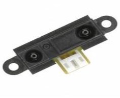 GP2Y0A21YK0F Distance Measuring Sensor: Datasheet, Schematic and Pinout
31 July 20217873
 SP505 Transceiver:Datasheet, Pinout, Operation Circuit
08 September 2021522
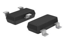
 TTA1943 VS. 2SA1943 How to Differentiate?
27 June 20227190
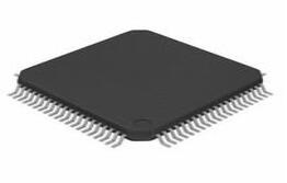
 STMicroelectronics STM32F051R8T7 Microcontroller Overview: Features and Applications
11 June 2025324
 OP27G OP-AMP: Application, Pinout and Datasheet
07 July 20218810
 LT1084 Regulator: Pinout, Equivalent and Datasheet
04 November 20213502
 Exploring the MCF51QU128 Microcontroller: Features, Specifications, and Applications
29 February 2024202
 Thermal Pads vs Thermal Paste Understanding the Key Differences
19 July 20252661
 What is an Oxygen Sensor?
24 April 202513246
 DoD Allocates $238 Million for Semiconductor Centers under CHIPS and Science Act
23 September 20232806
 Semiconductor Devices: Impact on IoT and Modern Communication (Part-1)
22 July 20242636
 DC Bias Characteristic of a Capacitor: Why MLCC Capacitance Drops Under Voltage
03 July 202612088
 Understanding the Crystal Oscillator: Construction, Working Principles and Applications
08 July 20244214
 Analog-to-Digital Converters (ADCs): Decrypting Resolutions and Sampling Rates
24 February 20225356
 How to Identify the Perfect Proximity Sensor for Your Application
19 July 20251739
Texas Instruments
In Stock
United States
China
Canada
Japan
Russia
Germany
United Kingdom
Singapore
Italy
Hong Kong(China)
Taiwan(China)
France
Korea
Mexico
Netherlands
Malaysia
Austria
Spain
Switzerland
Poland
Thailand
Vietnam
India
United Arab Emirates
Afghanistan
Åland Islands
Albania
Algeria
American Samoa
Andorra
Angola
Anguilla
Antigua & Barbuda
Argentina
Armenia
Aruba
Australia
Azerbaijan
Bahamas
Bahrain
Bangladesh
Barbados
Belarus
Belgium
Belize
Benin
Bermuda
Bhutan
Bolivia
Bonaire, Sint Eustatius and Saba
Bosnia & Herzegovina
Botswana
Brazil
British Indian Ocean Territory
British Virgin Islands
Brunei
Bulgaria
Burkina Faso
Burundi
Cabo Verde
Cambodia
Cameroon
Cayman Islands
Central African Republic
Chad
Chile
Christmas Island
Cocos (Keeling) Islands
Colombia
Comoros
Congo
Congo (DRC)
Cook Islands
Costa Rica
Côte d’Ivoire
Croatia
Cuba
Curaçao
Cyprus
Czechia
Denmark
Djibouti
Dominica
Dominican Republic
Ecuador
Egypt
El Salvador
Equatorial Guinea
Eritrea
Estonia
Eswatini
Ethiopia
Falkland Islands
Faroe Islands
Fiji
Finland
French Guiana
French Polynesia
Gabon
Gambia
Georgia
Ghana
Gibraltar
Greece
Greenland
Grenada
Guadeloupe
Guam
Guatemala
Guernsey
Guinea
Guinea-Bissau
Guyana
Haiti
Honduras
Hungary
Iceland
Indonesia
Iran
Iraq
Ireland
Isle of Man
Israel
Jamaica
Jersey
Jordan
Kazakhstan
Kenya
Kiribati
Kosovo
Kuwait
Kyrgyzstan
Laos
Latvia
Lebanon
Lesotho
Liberia
Libya
Liechtenstein
Lithuania
Luxembourg
Macao(China)
Madagascar
Malawi
Maldives
Mali
Malta
Marshall Islands
Martinique
Mauritania
Mauritius
Mayotte
Micronesia
Moldova
Monaco
Mongolia
Montenegro
Montserrat
Morocco
Mozambique
Myanmar
Namibia
Nauru
Nepal
New Caledonia
New Zealand
Nicaragua
Niger
Nigeria
Niue
Norfolk Island
North Korea
North Macedonia
Northern Mariana Islands
Norway
Oman
Pakistan
Palau
Palestinian Authority
Panama
Papua New Guinea
Paraguay
Peru
Philippines
Pitcairn Islands
Portugal
Puerto Rico
Qatar
Réunion
Romania
Rwanda
Samoa
San Marino
São Tomé & Príncipe
Saudi Arabia
Senegal
Serbia
Seychelles
Sierra Leone
Sint Maarten
Slovakia
Slovenia
Solomon Islands
Somalia
South Africa
South Sudan
Sri Lanka
St Helena, Ascension, Tristan da Cunha
St. Barthélemy
St. Kitts & Nevis
St. Lucia
St. Martin
St. Pierre & Miquelon
St. Vincent & Grenadines
Sudan
Suriname
Svalbard & Jan Mayen
Sweden
Syria
Tajikistan
Tanzania
Timor-Leste
Togo
Tokelau
Tonga
Trinidad & Tobago
Tunisia
Turkey
Turkmenistan
Turks & Caicos Islands
Tuvalu
U.S. Outlying Islands
U.S. Virgin Islands
Uganda
Ukraine
Uruguay
Uzbekistan
Vanuatu
Vatican City
Venezuela
Wallis & Futuna
Yemen
Zambia
Zimbabwe
![LMV722MX]() LMV722MX
LMV722MXTexas Instruments
![LMC6082AIN]() LMC6082AIN
LMC6082AINTexas Instruments
![RC4558P]() RC4558P
RC4558PTexas Instruments
![LMC6482IMM/NOPB]() LMC6482IMM/NOPB
LMC6482IMM/NOPBTexas Instruments
![LM324MX/NOPB]() LM324MX/NOPB
LM324MX/NOPBTexas Instruments
![LM324AM/NOPB]() LM324AM/NOPB
LM324AM/NOPBTexas Instruments
![LMV324IDR]() LMV324IDR
LMV324IDRTexas Instruments
![LMC7101BIM5/NOPB]() LMC7101BIM5/NOPB
LMC7101BIM5/NOPBTexas Instruments
![TLV2372IDR]() TLV2372IDR
TLV2372IDRTexas Instruments
![NE5532P]() NE5532P
NE5532PTexas Instruments


