
 Product
 Brand
Brand Articles
 Tools
Tools
AD8307 92 dB Logarithmic Amplifier: Datasheet, Pinout, and RF Power Measurement Analysis

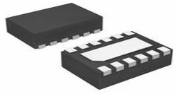
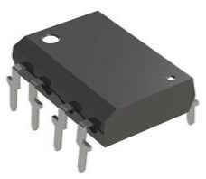
Tin 5V 8 Amplifier AD8307 8 Pin 5V 8-SOIC (0.154, 3.90mm Width)
Unit Price: $26.640729
Ext Price: $26.64


Tin 5V 8 Amplifier AD8307 8 Pin 5V 8-SOIC (0.154, 3.90mm Width)
Master RF power measurement with the AD8307. Featuring a 92 dB dynamic range and 500 MHz bandwidth, this log amp is ideal for RSSI. View specs and design today.
- Executive Summary: What is the AD8307?
- 1. Technical Specifications & Performance Analysis
- 2. Pinout, Package, and Configuration
- 3. Design & Integration Guide (For Engineers & Makers)
- 4. Typical Applications & Use Cases
- 5. Alternatives and Cross-Reference Guide
- 6. Frequently Asked Questions (FAQ)
- 7. Resources
- Specifications
- Parts with Similar Specs
- Datasheet PDF
Executive Summary: What is the AD8307?
The AD8307 is a low-cost, complete 500 MHz monolithic demodulating logarithmic amplifier designed for signal power measurement and signal compression in RF and IF systems. It converts an input signal into a decibel-scaled DC voltage output, making it an essential component for measuring signal strength over a vast range.
Market Position: High-performance, industry-standard legacy part; widely considered the "gold standard" for low-cost RF power detection.
Top Features: Massive 92 dB dynamic range, wide frequency operation from DC to 500 MHz, and low power consumption (7.5 mA).
Primary Audience: Ideal for RF design engineers, telecommunications infrastructure developers, and advanced hobbyists building test equipment like spectrum analyzers.
Supply Status: Active; widely available through major distributors.
1. Technical Specifications & Performance Analysis
The AD8307 stands out because it provides a highly linear logarithmic response across a wide dynamic range, which is difficult to achieve with discrete components.
1.1 Core Architecture (Demodulating Log Amp)
The AD8307 utilizes a "progressive compression" or "successive detection" architecture. This involves a chain of amplifier/limiter cells that rectify the signal at each stage. This design allows the chip to maintain high sensitivity (-75 dBm) while handling relatively high power (+17 dBm) without damage, providing a stable 25 mV/dB slope.
1.2 Key Electrical Characteristics
Engineers must account for the following power and thermal parameters during BOM selection:
Supply Voltage: Operates on a single supply between 2.7 V and 5.5 V, making it compatible with both 3.3V and 5V logic systems.
Supply Current: Typically consumes only 7.5 mA, making it suitable for handheld battery-operated instruments.
Logarithmic Slope: Precision-trimmed to 25 mV/dB, ensuring easy conversion from voltage to dBm in software.
Log Intercept: Calibrated to -84 dBm.
1.3 Interfaces and Connectivity
The AD8307 is a purely analog device. It features differential inputs (INP, INN) and a single-ended voltage output (VOUT). While it does not have a digital bus like SPI or I2C, its analog output is easily interfaced with the ADC of an Arduino, STM32, or ESP32 for digital processing.
2. Pinout, Package, and Configuration
The AD8307 is known for its simplicity, requiring very few external components to function.
2.1 Pin Configuration Guide

INP (Pin 1): Positive input signal.
INN (Pin 2): Negative input signal (usually AC coupled to ground for single-ended use).
COM (Pin 3): Common/Ground.
VOUT (Pin 4): Logarithmic output voltage.
ENB (Pin 5): Enable/Power-down. Pull high for operation, low for standby.
VPOS (Pin 6): Positive supply voltage (2.7V to 5.5V).
OFS (Pin 7): Offset compensation (used for low-frequency stability).
COM (Pin 8): Common/Ground.
2.2 Naming Convention & Ordering Codes
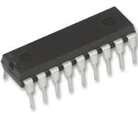
AD8307AN: Plastic Dual-in-Line Package (DIP-8). Preferred for breadboarding and prototyping.
AD8307AR: Small Outline Integrated Circuit (SOIC-8). Standard for surface-mount production.
AD8307ARZ: "Z" suffix indicates RoHS compliance (Lead-free).
2.3 Available Packages
| Package Type | Dimensions | Common Use Case |
|---|---|---|
| PDIP-8 | 9.27mm x 6.35mm | Prototyping, Through-hole PCB |
| SOIC-8 | 4.90mm x 3.91mm | Compact commercial electronics |
3. Design & Integration Guide (For Engineers & Makers)
Pro Tip: Always verify pin compatibility and input matching before migrating from older diode-based detectors.
3.1 Hardware Implementation
Bypass Capacitors: Use a 0.1 µF ceramic capacitor in parallel with a 100 pF capacitor as close to the VPOS pin as possible to filter high-frequency noise.
Input Coupling: Use high-quality capacitors (e.g., 10nF) for AC coupling signals into the INP and INN pins.
PCB Layout: Use a solid ground plane. Keep input traces as short as possible to prevent the AD8307 from picking up stray RF interference.
3.2 Common Design Challenges
Issue: Input Impedance Mismatch: The AD8307 has a high input impedance (~1.1 kΩ), but most RF systems are 50 Ω.
Fix: Place a 52.3 Ω resistor in parallel across the input to ground to provide a wideband 50 Ω match.
Issue: Environmental Noise: Because it is so sensitive (-75 dBm), it can detect Wi-Fi or cellular signals even without an antenna.
Fix: Enclose the AD8307 circuit in a shielded metal "can" or box.
Issue: DC Offset at Low Frequency: At frequencies near DC, the internal offset can cause errors.
Fix: Connect a large capacitor (e.g., 10 µF) to the OFS pin (Pin 7) to stabilize the internal feedback loop.
4. Typical Applications & Use Cases
🎬 Watch Tutorial: AD8307
4.1 Real-World Example: RF Power Meter
In a handheld RF Power Meter, the AD8307 acts as the "front end." An antenna picks up a signal, which passes through a 50 Ω matching resistor into the AD8307. The chip outputs a voltage (e.g., 2.0V for 0 dBm). A microcontroller reads this voltage via its ADC and displays the power level in dBm on an LCD.
5. Alternatives and Cross-Reference Guide
If the AD8307 is unavailable or doesn't meet your frequency requirements, consider these alternatives:
Direct Replacements: There are no 100% pin-compatible clones from other manufacturers, but the AD8310 is a faster version with a similar footprint.
Better Performance: ADL5513 or AD8318 offer higher frequency ranges (up to 4 GHz or 8 GHz).
Cost-Effective Options: LT5537 (Analog Devices/Linear Tech) offers a similar dynamic range and frequency response.
6. Frequently Asked Questions (FAQ)
Q: What is the difference between AD8307 and AD8310?
A: The AD8310 is faster (response time of 15ns vs 500ns) and has a wider bandwidth (up to 440 MHz with better linearity), but it consumes more current.
Q: Can AD8307 be used for audio signals?
A: Yes, it works down to DC. However, you must use large coupling capacitors and utilize the OFS (offset) pin to prevent DC drift from affecting the measurement.
Q: Where can I find the AD8307 datasheet and CAD models?
A: The official datasheet is available on the Analog Devices website. Footprints for Altium, KiCad, and Eagle are typically available via SnapEDA or Ultra Librarian.
Q: Is the AD8307 suitable for battery-operated devices?
A: Absolutely. With a 7.5 mA typical current draw and a power-down mode (ENB pin), it is highly efficient for portable use.
7. Resources
Application Note: AN-691 (Low-cost RF power measurement)
Evaluation Boards: AD8307-EVALZ
Specifications
Parts with Similar Specs
- ImagePart NumberManufacturerPackage / CaseNumber of PinsInput Offset Voltage (Vos)Min Supply VoltageSupply VoltageMax Supply VoltageOperating Supply CurrentMoisture Sensitivity Level (MSL)View Compare
![AD8307ARZ-REEL]()
AD8307ARZ-REEL
8-SOIC (0.154, 3.90mm Width)
8
500 μV
2.7 V
5 V
5.5 V
8 mA
1 (Unlimited)
![AD8307AR-REEL]()
8-SOIC (0.154, 3.90mm Width)
8
500 μV
2.7 V
5 V
5.5 V
8 mA
1 (Unlimited)
![AD8307AR]()
8-SOIC (0.154, 3.90mm Width)
8
500 μV
2.7 V
5 V
5.5 V
8 mA
1 (Unlimited)
![AD8307AR-REEL7]()
8-SOIC (0.154, 3.90mm Width)
8
500 μV
2.7 V
5 V
5.5 V
8 mA
1 (Unlimited)

Datasheet PDF
- Datasheets :
- ConflictMineralStatement :
 LIS2DE12TR Motion Sensor: Three-Axis Accelerometer, Datasheet, Application Hint
26 February 20222267
 DRV8835 IC: Pinout, Feature and Application
03 August 20214407
 TPS7B6950QDBVRQ1 Regulator: Equivalents, Pinout
25 March 2022805
 2SB817 PNP Power Transistor: B817 Power Transistor, Datasheet pdf and Equivalent
15 December 202113152
 ULN2803A Transistor Array: Pinout, Circuit, and Datasheet
15 June 202121294
 STM32F070CBT6 ARM Microcontroller: Pinout, Datasheet, Features and Applications
06 January 20222121
 IRF1404 Power MOSFET: Datasheet, IRF1404, IRF1404 vs. IRF3205
24 November 202119248
 TLP250 Photocoupler: Schematic, Pinout and Datasheet
11 September 202118418
 Introduction to Reluctance Motor
08 March 20216193
 What is RF Filter?
09 December 20219585
 AI Server MLCCs: Why NVIDIA Rubin Racks Require Over 600,000 Capacitors
02 June 20261791
 How Do We Seize Investment Opportunities on the Eve of the Ultimate Human Energy Final?
12 July 20222226
 What is An Optoisolator?
09 January 20218410
 Electronic Components in Aerospace Aircraft
15 March 20243980
 What are Proximity Sensors?
24 October 20258437
 Supercapacitors Explained: How EDLC, Pseudo, and Hybrid Capacitors Store Power
23 June 202610664
Analog Devices Inc.
In Stock: 2830
Minimum: 1 Multiples: 1
Qty
Unit Price
Ext Price
1
$26.640729
$26.64
10
$25.132763
$251.33
100
$23.710154
$2,371.02
500
$22.368070
$11,184.04
1000
$21.101953
$21,101.95
Not the price you want? Send RFQ Now and we'll contact you ASAP.
Inquire for More Quantity
![AD8138ARZ]() AD8138ARZ
AD8138ARZAnalog Devices Inc.
![AD8138ARMZ]() AD8138ARMZ
AD8138ARMZAnalog Devices Inc.
![AD8310ARMZ]() AD8310ARMZ
AD8310ARMZAnalog Devices Inc.
![ADA4941-1YRZ]() ADA4941-1YRZ
ADA4941-1YRZAnalog Devices Inc.
![AD8309ARUZ]() AD8309ARUZ
AD8309ARUZAnalog Devices Inc.
![AD8331ARQZ]() AD8331ARQZ
AD8331ARQZAnalog Devices Inc.
![AD8138ARZ-R7]() AD8138ARZ-R7
AD8138ARZ-R7Analog Devices Inc.
![AD8138ARMZ-REEL7]() AD8138ARMZ-REEL7
AD8138ARMZ-REEL7Analog Devices Inc.
![AD8310ARMZ-REEL7]() AD8310ARMZ-REEL7
AD8310ARMZ-REEL7Analog Devices Inc.
![AD8307ARZ]() AD8307ARZ
AD8307ARZAnalog Devices Inc.


