
 Product
 Brand
Brand Articles
 Tools
Tools
J310 Transistor: J310 Pinout, Datasheet, J310 RF Amplifier


JFET N-CH 25V 60MA TO92
J310 is an N-Channel RF amplifier. This article will unlock more details about J310. There is a huge range of Semiconductors, Capacitors, Resistors and ICs in stock. Welcome RFQ.

Follow on Experiment with the J310 JFET
J310 Pinout

J310 Pinout
J310 CAD Model
Symbol

J310 Symbol
Footprint

J310 Footprint
3D Model

J310 3D Model
J310 Description
The J310 is an N-Channel RF amplifier. This device is designed for VHF/UHF amplifier, oscillator and mixer applications. As a common gate amplifier, 16 dB at 100 MHz and 12 dB at 450 MHz can be realized.
J310 Feature
N-channel JFET for VHF / UHF amplification applications, oscillators and mixers
Voltage max. drain-source V DS = 25 V
Voltage max. gate-source V GS = 25 V
Current max. live gate I GF = 10 mA
Power max. P D = 350 mW
Package: TO-92
J310 Equivalent
The equivalent for J310:
NTE2902
2902
J309
Specifications
- TypeParameter
- Lifecycle Status
Lifecycle Status refers to the current stage of an electronic component in its product life cycle, indicating whether it is active, obsolete, or transitioning between these states. An active status means the component is in production and available for purchase. An obsolete status indicates that the component is no longer being manufactured or supported, and manufacturers typically provide a limited time frame for support. Understanding the lifecycle status is crucial for design engineers to ensure continuity and reliability in their projects.
LAST SHIPMENTS (Last Updated: 20 hours ago) - Mount
In electronic components, the term "Mount" typically refers to the method or process of physically attaching or fixing a component onto a circuit board or other electronic device. This can involve soldering, adhesive bonding, or other techniques to secure the component in place. The mounting process is crucial for ensuring proper electrical connections and mechanical stability within the electronic system. Different components may have specific mounting requirements based on their size, shape, and function, and manufacturers provide guidelines for proper mounting procedures to ensure optimal performance and reliability of the electronic device.
Through Hole - Package / Case
refers to the protective housing that encases an electronic component, providing mechanical support, electrical connections, and thermal management.
TO-226-3, TO-92-3 (TO-226AA) - Number of Pins3
- Weight201mg
- Breakdown Voltage / V-25V
- Number of Elements1
- Packaging
Semiconductor package is a carrier / shell used to contain and cover one or more semiconductor components or integrated circuits. The material of the shell can be metal, plastic, glass or ceramic.
Bulk - JESD-609 Code
The "JESD-609 Code" in electronic components refers to a standardized marking code that indicates the lead-free solder composition and finish of electronic components for compliance with environmental regulations.
e0 - Pbfree Code
The "Pbfree Code" parameter in electronic components refers to the code or marking used to indicate that the component is lead-free. Lead (Pb) is a toxic substance that has been widely used in electronic components for many years, but due to environmental concerns, there has been a shift towards lead-free alternatives. The Pbfree Code helps manufacturers and users easily identify components that do not contain lead, ensuring compliance with regulations and promoting environmentally friendly practices. It is important to pay attention to the Pbfree Code when selecting electronic components to ensure they meet the necessary requirements for lead-free applications.
no - Part Status
Parts can have many statuses as they progress through the configuration, analysis, review, and approval stages.
Obsolete - Moisture Sensitivity Level (MSL)
Moisture Sensitivity Level (MSL) is a standardized rating that indicates the susceptibility of electronic components, particularly semiconductors, to moisture-induced damage during storage and the soldering process, defining the allowable exposure time to ambient conditions before they require special handling or baking to prevent failures
1 (Unlimited) - Number of Terminations3
- Termination
Termination in electronic components refers to the practice of matching the impedance of a circuit to prevent signal reflections and ensure maximum power transfer. It involves the use of resistors or other components at the end of transmission lines or connections. Proper termination is crucial in high-frequency applications to maintain signal integrity and reduce noise.
Through Hole - Terminal Finish
Terminal Finish refers to the surface treatment applied to the terminals or leads of electronic components to enhance their performance and longevity. It can improve solderability, corrosion resistance, and overall reliability of the connection in electronic assemblies. Common finishes include nickel, gold, and tin, each possessing distinct properties suitable for various applications. The choice of terminal finish can significantly impact the durability and effectiveness of electronic devices.
Tin/Lead (Sn/Pb) - Max Operating Temperature
The Maximum Operating Temperature is the maximum body temperature at which the thermistor is designed to operate for extended periods of time with acceptable stability of its electrical characteristics.
150°C - Min Operating Temperature
The "Min Operating Temperature" parameter in electronic components refers to the lowest temperature at which the component is designed to operate effectively and reliably. This parameter is crucial for ensuring the proper functioning and longevity of the component, as operating below this temperature may lead to performance issues or even damage. Manufacturers specify the minimum operating temperature to provide guidance to users on the environmental conditions in which the component can safely operate. It is important to adhere to this parameter to prevent malfunctions and ensure the overall reliability of the electronic system.
-55°C - ColorOrange
- HTS Code
HTS (Harmonized Tariff Schedule) codes are product classification codes between 8-1 digits. The first six digits are an HS code, and the countries of import assign the subsequent digits to provide additional classification. U.S. HTS codes are 1 digits and are administered by the U.S. International Trade Commission.
8541.21.00.75 - Voltage - Rated DC
Voltage - Rated DC is a parameter that specifies the maximum direct current (DC) voltage that an electronic component can safely handle without being damaged. This rating is crucial for ensuring the proper functioning and longevity of the component in a circuit. Exceeding the rated DC voltage can lead to overheating, breakdown, or even permanent damage to the component. It is important to carefully consider this parameter when designing or selecting components for a circuit to prevent any potential issues related to voltage overload.
25V - Max Power Dissipation
The maximum power that the MOSFET can dissipate continuously under the specified thermal conditions.
625mW - Terminal Position
In electronic components, the term "Terminal Position" refers to the physical location of the connection points on the component where external electrical connections can be made. These connection points, known as terminals, are typically used to attach wires, leads, or other components to the main body of the electronic component. The terminal position is important for ensuring proper connectivity and functionality of the component within a circuit. It is often specified in technical datasheets or component specifications to help designers and engineers understand how to properly integrate the component into their circuit designs.
BOTTOM - Peak Reflow Temperature (Cel)
Peak Reflow Temperature (Cel) is a parameter that specifies the maximum temperature at which an electronic component can be exposed during the reflow soldering process. Reflow soldering is a common method used to attach electronic components to a circuit board. The Peak Reflow Temperature is crucial because it ensures that the component is not damaged or degraded during the soldering process. Exceeding the specified Peak Reflow Temperature can lead to issues such as component failure, reduced performance, or even permanent damage to the component. It is important for manufacturers and assemblers to adhere to the recommended Peak Reflow Temperature to ensure the reliability and functionality of the electronic components.
240 - Reach Compliance Code
Reach Compliance Code refers to a designation indicating that electronic components meet the requirements set by the Registration, Evaluation, Authorization, and Restriction of Chemicals (REACH) regulation in the European Union. It signifies that the manufacturer has assessed and managed the chemical substances within the components to ensure safety and environmental protection. This code is vital for compliance with regulations aimed at minimizing risks associated with hazardous substances in electronic products.
not_compliant - Current Rating
Current rating is the maximum current that a fuse will carry for an indefinite period without too much deterioration of the fuse element.
10mA - Frequency
In electronic components, the parameter "Frequency" refers to the rate at which a signal oscillates or cycles within a given period of time. It is typically measured in Hertz (Hz) and represents how many times a signal completes a full cycle in one second. Frequency is a crucial aspect in electronic components as it determines the behavior and performance of various devices such as oscillators, filters, and communication systems. Understanding the frequency characteristics of components is essential for designing and analyzing electronic circuits to ensure proper functionality and compatibility with other components in a system.
100MHz - Time@Peak Reflow Temperature-Max (s)
Time@Peak Reflow Temperature-Max (s) refers to the maximum duration that an electronic component can be exposed to the peak reflow temperature during the soldering process, which is crucial for ensuring reliable solder joint formation without damaging the component.
30 - Base Part Number
The "Base Part Number" (BPN) in electronic components serves a similar purpose to the "Base Product Number." It refers to the primary identifier for a component that captures the essential characteristics shared by a group of similar components. The BPN provides a fundamental way to reference a family or series of components without specifying all the variations and specific details.
J310 - Pin Count
a count of all of the component leads (or pins)
3 - Qualification Status
An indicator of formal certification of qualifications.
Not Qualified - Element Configuration
The distribution of electrons of an atom or molecule (or other physical structure) in atomic or molecular orbitals.
Single - Operating Mode
A phase of operation during the operation and maintenance stages of the life cycle of a facility.
DEPLETION MODE - Power Dissipation
the process by which an electronic or electrical device produces heat (energy loss or waste) as an undesirable derivative of its primary action.
350mW - Current - Test
Current - Test is a parameter in electronic components that refers to the maximum current that the component can handle during testing without being damaged. This parameter is crucial for determining the operational limits of the component and ensuring its reliability under specified conditions. It is typically specified in the component's datasheet and is important for designers and engineers to consider when designing circuits to prevent overloading the component. Testing the component at or below the specified "Current - Test" value helps ensure its proper functioning and longevity in the intended application.
10mA - Transistor Application
In the context of electronic components, the parameter "Transistor Application" refers to the specific purpose or function for which a transistor is designed and used. Transistors are semiconductor devices that can amplify or switch electronic signals and are commonly used in various electronic circuits. The application of a transistor can vary widely depending on its design and characteristics, such as whether it is intended for audio amplification, digital logic, power control, or radio frequency applications. Understanding the transistor application is important for selecting the right type of transistor for a particular circuit or system to ensure optimal performance and functionality.
AMPLIFIER - Drain to Source Voltage (Vdss)
The Drain to Source Voltage (Vdss) is a key parameter in electronic components, particularly in field-effect transistors (FETs) such as MOSFETs. It refers to the maximum voltage that can be applied between the drain and source terminals of the FET without causing damage to the component. Exceeding this voltage limit can lead to breakdown and potentially permanent damage to the device.Vdss is an important specification to consider when designing or selecting components for a circuit, as it determines the operating range and reliability of the FET. It is crucial to ensure that the Vdss rating of the component is higher than the maximum voltage expected in the circuit to prevent failures and ensure proper functionality.In summary, the Drain to Source Voltage (Vdss) is a critical parameter that defines the maximum voltage tolerance of a FET component and plays a significant role in determining the overall performance and reliability of electronic circuits.
25V - Transistor Type
Transistor type refers to the classification of transistors based on their operation and construction. The two primary types are bipolar junction transistors (BJTs) and field-effect transistors (FETs). BJTs use current to control the flow of current, while FETs utilize voltage to control current flow. Each type has its own subtypes, such as NPN and PNP for BJTs, and MOSFETs and JFETs for FETs, impacting their applications and characteristics in electronic circuits.
N-Channel JFET - Continuous Drain Current (ID)
Continuous Drain Current (ID) is a key parameter in electronic components, particularly in field-effect transistors (FETs) such as MOSFETs. It refers to the maximum current that can flow continuously through the drain terminal of the FET without causing damage to the component. This parameter is crucial for determining the power handling capability of the FET and is specified by the manufacturer in the component's datasheet. Designers must ensure that the actual operating current does not exceed the specified Continuous Drain Current to prevent overheating and potential failure of the component.
60mA - Gate to Source Voltage (Vgs)
The Gate to Source Voltage (Vgs) is a crucial parameter in electronic components, particularly in field-effect transistors (FETs) such as MOSFETs. It refers to the voltage difference between the gate and source terminals of the FET. This voltage determines the conductivity of the FET and controls the flow of current through the device. By varying the Vgs, the FET can be switched on or off, allowing for precise control of electronic circuits. Understanding and properly managing the Vgs is essential for ensuring the reliable and efficient operation of FET-based circuits.
-25V - Gain
In electronic components, "Gain" refers to the ratio of the output signal amplitude to the input signal amplitude. It is a measure of the amplification provided by the component, such as a transistor or operational amplifier. Gain is typically expressed in decibels (dB) or as a numerical value, indicating how much the signal is amplified by the component.A higher gain value indicates a greater amplification of the input signal, while a lower gain value indicates less amplification. Gain is an important parameter in designing and analyzing electronic circuits, as it determines the overall performance and functionality of the system. Different components have different gain characteristics, and understanding the gain of a component is crucial for achieving the desired signal processing or amplification in electronic systems.
16dB - Drain to Source Breakdown Voltage
Drain to Source Breakdown Voltage, often denoted as V(BR) D-S, is a critical parameter in electronic components, particularly in field-effect transistors (FETs) and metal-oxide-semiconductor FETs (MOSFETs). It represents the maximum voltage that can be applied between the drain and source terminals of the device without causing breakdown or permanent damage. Exceeding this voltage can lead to excessive current flow, resulting in thermal failure or destruction of the component. It is essential for ensuring reliable operation in circuit designs where high voltages may be encountered.
25V - FET Technology
Field-Effect Transistor (FET) technology is a type of semiconductor device commonly used in electronic components such as transistors and integrated circuits. FETs operate by controlling the flow of current through a semiconductor channel using an electric field. There are several types of FETs, including Metal-Oxide-Semiconductor FETs (MOSFETs) and Junction FETs (JFETs), each with its own characteristics and applications. FET technology offers advantages such as high input impedance, low power consumption, and fast switching speeds, making it suitable for a wide range of electronic devices and circuits. Overall, FET technology plays a crucial role in modern electronics by enabling efficient and reliable signal processing and amplification.
JUNCTION - Noise Figure
Noise figure (NF) and noise factor (F) are measures of degradation of the signal-to-noise ratio (SNR), caused by components in a signal chain.
3 dB - Voltage - Test
Voltage - Test is a parameter used to specify the maximum voltage that an electronic component can withstand during testing without experiencing damage or failure. This parameter is crucial for ensuring the reliability and safety of the component in various operating conditions. It is typically measured in volts and is important for determining the suitability of the component for specific applications where voltage levels may vary. Manufacturers provide this information in datasheets to help engineers and designers select the appropriate components for their circuits based on the voltage requirements. It is essential to adhere to the specified voltage limits to prevent potential damage to the component and ensure proper functionality.
10V - Feedback Cap-Max (Crss)
Feedback Cap-Max (Crss) refers to the maximum capacitance between the output and input of an electronic component, such as a transistor or an operational amplifier. It indicates the level of feedback capacitance that can negatively affect the performance, stability, and bandwidth of the device. A higher Crss value may introduce unintended phase shifts or frequency response issues, making it crucial to consider in circuit design to ensure optimal operation.
2.5 pF - Height5.33mm
- Length5.2mm
- Width4.19mm
- REACH SVHC
The parameter "REACH SVHC" in electronic components refers to the compliance with the Registration, Evaluation, Authorization, and Restriction of Chemicals (REACH) regulation regarding Substances of Very High Concern (SVHC). SVHCs are substances that may have serious effects on human health or the environment, and their use is regulated under REACH to ensure their safe handling and minimize their impact.Manufacturers of electronic components need to declare if their products contain any SVHCs above a certain threshold concentration and provide information on the safe use of these substances. This information allows customers to make informed decisions about the potential risks associated with using the components and take appropriate measures to mitigate any hazards.Ensuring compliance with REACH SVHC requirements is essential for electronics manufacturers to meet regulatory standards, protect human health and the environment, and maintain transparency in their supply chain. It also demonstrates a commitment to sustainability and responsible manufacturing practices in the electronics industry.
No SVHC - RoHS Status
RoHS means “Restriction of Certain Hazardous Substances” in the “Hazardous Substances Directive” in electrical and electronic equipment.
Non-RoHS Compliant - Lead Free
Lead Free is a term used to describe electronic components that do not contain lead as part of their composition. Lead is a toxic material that can have harmful effects on human health and the environment, so the electronics industry has been moving towards lead-free components to reduce these risks. Lead-free components are typically made using alternative materials such as silver, copper, and tin. Manufacturers must comply with regulations such as the Restriction of Hazardous Substances (RoHS) directive to ensure that their products are lead-free and environmentally friendly.
Lead Free
Parts with Similar Specs
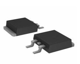
J310 Package

J310 Package
J310 Manufacturer
ON Semiconductor (Nasdaq: ON) is driving energy efficient innovations, empowering customers to reduce global energy use. The company offers a comprehensive portfolio of energy-efficient power and signal management, logic, discrete and custom solutions to help design engineers solve their unique design challenges in automotive, communications, computing, consumer, industrial, LED lighting, medical, military/aerospace and power supply applications.
ON Semiconductor operates a responsive, reliable, world-class supply chain and quality program, and a network of manufacturing facilities, sales offices and design centres in key markets throughout North America, Europe, and the Asia Pacific regions.
Datasheet PDF
- PCN Obsolescence/ EOL :
- Datasheets :
J310-ON-Semiconductor-datasheet-21648.pdf
J310-ON-Semiconductor-datasheet-55001.pdf
J310-Fairchild-Semiconductor-datasheet-7537324.pdf
J310-Fairchild-datasheet-13026.pdf
J310-Fairchild-Semiconductor-datasheet-10328222.pdf
J310-ON-Semiconductor-datasheet-156348.pdf
J310-Fairchild-Semiconductor-datasheet-14042903.pdf
J310-ON-Semiconductor-datasheet-654839.pdf
- ReachStatement :
What is the J310 JFET?
his is a further progression in the application of the J310 JFET in high-performance preamplifiers. This one is designed to amplify the 20KHz to >30 MHz range, uses the premium J310 FET and 2N5109 CATV bipolar transistors, giving a good combination of low thermal noise, gain and IMD resistance.
What is the pinout for the J310 device?
J310 PINOUT: Hold the device with leads pointing toward you with flat face up--left to right--drain, source,gate (the device is not symmetrical, i.e. source and drain cannot
Is the J310 a high IDSS device?
The J310 is a high-Idss device, much higher than the general JFETs like your MPF102, 2N3819, 2N4416, etc. It's also the defacto device (along with the same die in a metal can, the U310 which is what I use) for almost all active whip-amps that use a JFET as the input device.
 IRF640S Power MOSFET: Datasheet, IRF640 MOSFET, Pinout
11 August 20212053
 25AA160D 16K SPI Bus Serial EEPROM: Pinout, Equivalent and Datasheet
21 April 20221524
![RP2040 VS ESP32[Video+FAQ]: Which one is better?](https://res.utmel.com/Images/Article/a7926785-e416-4bc7-a497-2b286c021b7c.jpg) RP2040 VS ESP32[Video+FAQ]: Which one is better?
RP2040 VS ESP32[Video+FAQ]: Which one is better?03 March 2022185795
 73S1215F System-on-Chip: Technical Specifications and Applications
29 February 2024163
 STM32H743XIH6 Review: High-Performance 480MHz ARM Cortex-M7 Microcontroller Comparison Guide
24 July 20255022
 Designing Ultra-Compact Electronics with ATTINY10: Specs, Pinout, and TPI Programming
06 February 202688
 A Comprehensive Guide to the AD558 Digital to Analog Converter (DAC)
06 March 2024774
![CDSOT23-SM712 Tvs Diode Surface SOT-23-3 14V Clamp[FAQ]: Datasheet, Pinout, and Applications](https://res.utmel.com/Images/Article/9fea5c62-7b3d-490f-89eb-f71899f86d2b.png) CDSOT23-SM712 Tvs Diode Surface SOT-23-3 14V Clamp[FAQ]: Datasheet, Pinout, and Applications
CDSOT23-SM712 Tvs Diode Surface SOT-23-3 14V Clamp[FAQ]: Datasheet, Pinout, and Applications02 April 20222304
 What are Comparators?
03 December 20205505
 Laser diodes or LEDs what sets them apart
14 July 2025974
 Understanding the Low Noise Amplifier (LNA)
20 March 202522564
 How Do We Seize Investment Opportunities on the Eve of the Ultimate Human Energy Final?
12 July 20222171
 Role of Solar Energy in Wide-Band Gap Devices for Photovoltaic Applications
15 March 20244205
 How does a Photodiode Work?
15 August 202021623
 Applications of Sensors on CNC Machine Tools
13 September 202118896
 Using ESP32 to Make an IoT Weather Station
24 February 20236455
ON Semiconductor
In Stock: 50
United States
China
Canada
Japan
Russia
Germany
United Kingdom
Singapore
Italy
Hong Kong(China)
Taiwan(China)
France
Korea
Mexico
Netherlands
Malaysia
Austria
Spain
Switzerland
Poland
Thailand
Vietnam
India
United Arab Emirates
Afghanistan
Åland Islands
Albania
Algeria
American Samoa
Andorra
Angola
Anguilla
Antigua & Barbuda
Argentina
Armenia
Aruba
Australia
Azerbaijan
Bahamas
Bahrain
Bangladesh
Barbados
Belarus
Belgium
Belize
Benin
Bermuda
Bhutan
Bolivia
Bonaire, Sint Eustatius and Saba
Bosnia & Herzegovina
Botswana
Brazil
British Indian Ocean Territory
British Virgin Islands
Brunei
Bulgaria
Burkina Faso
Burundi
Cabo Verde
Cambodia
Cameroon
Cayman Islands
Central African Republic
Chad
Chile
Christmas Island
Cocos (Keeling) Islands
Colombia
Comoros
Congo
Congo (DRC)
Cook Islands
Costa Rica
Côte d’Ivoire
Croatia
Cuba
Curaçao
Cyprus
Czechia
Denmark
Djibouti
Dominica
Dominican Republic
Ecuador
Egypt
El Salvador
Equatorial Guinea
Eritrea
Estonia
Eswatini
Ethiopia
Falkland Islands
Faroe Islands
Fiji
Finland
French Guiana
French Polynesia
Gabon
Gambia
Georgia
Ghana
Gibraltar
Greece
Greenland
Grenada
Guadeloupe
Guam
Guatemala
Guernsey
Guinea
Guinea-Bissau
Guyana
Haiti
Honduras
Hungary
Iceland
Indonesia
Iran
Iraq
Ireland
Isle of Man
Israel
Jamaica
Jersey
Jordan
Kazakhstan
Kenya
Kiribati
Kosovo
Kuwait
Kyrgyzstan
Laos
Latvia
Lebanon
Lesotho
Liberia
Libya
Liechtenstein
Lithuania
Luxembourg
Macao(China)
Madagascar
Malawi
Maldives
Mali
Malta
Marshall Islands
Martinique
Mauritania
Mauritius
Mayotte
Micronesia
Moldova
Monaco
Mongolia
Montenegro
Montserrat
Morocco
Mozambique
Myanmar
Namibia
Nauru
Nepal
New Caledonia
New Zealand
Nicaragua
Niger
Nigeria
Niue
Norfolk Island
North Korea
North Macedonia
Northern Mariana Islands
Norway
Oman
Pakistan
Palau
Palestinian Authority
Panama
Papua New Guinea
Paraguay
Peru
Philippines
Pitcairn Islands
Portugal
Puerto Rico
Qatar
Réunion
Romania
Rwanda
Samoa
San Marino
São Tomé & Príncipe
Saudi Arabia
Senegal
Serbia
Seychelles
Sierra Leone
Sint Maarten
Slovakia
Slovenia
Solomon Islands
Somalia
South Africa
South Sudan
Sri Lanka
St Helena, Ascension, Tristan da Cunha
St. Barthélemy
St. Kitts & Nevis
St. Lucia
St. Martin
St. Pierre & Miquelon
St. Vincent & Grenadines
Sudan
Suriname
Svalbard & Jan Mayen
Sweden
Syria
Tajikistan
Tanzania
Timor-Leste
Togo
Tokelau
Tonga
Trinidad & Tobago
Tunisia
Turkey
Turkmenistan
Turks & Caicos Islands
Tuvalu
U.S. Outlying Islands
U.S. Virgin Islands
Uganda
Ukraine
Uruguay
Uzbekistan
Vanuatu
Vatican City
Venezuela
Wallis & Futuna
Yemen
Zambia
Zimbabwe
![MMBFJ310LT1G]() MMBFJ310LT1G
MMBFJ310LT1GON Semiconductor
![MMBFJ309LT1G]() MMBFJ309LT1G
MMBFJ309LT1GON Semiconductor
![MMBF5484]() MMBF5484
MMBF5484ON Semiconductor
![2SK3557-6-TB-E]() 2SK3557-6-TB-E
2SK3557-6-TB-EON Semiconductor
![MMBF4416A]() MMBF4416A
MMBF4416AON Semiconductor
![MMBF5485]() MMBF5485
MMBF5485ON Semiconductor
![SMMBFJ310LT1G]() SMMBFJ310LT1G
SMMBFJ310LT1GON Semiconductor
![MMBFJ211]() MMBFJ211
MMBFJ211ON Semiconductor
![MMBFJ309]() MMBFJ309
MMBFJ309ON Semiconductor


