
 Product
 Brand
Brand Articles
 Tools
Tools
PCF8591 A/D and D/A Converter: Datasheet, PCF8591 Raspberry Pi, Interfacing

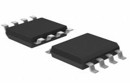
Tape & Reel (TR) Active 8 b b 11.1k k Special Purpose ADCs/DACs I2C, Serial 2.5V~6V V 16-SOIC (0.295, 7.50mm Width) Surface Mount


Tape & Reel (TR) Active 8 b b 11.1k k Special Purpose ADCs/DACs I2C, Serial 2.5V~6V V 16-SOIC (0.295, 7.50mm Width) Surface Mount
The PCF8591 is a single-chip, single-supply low-power 8-bit CMOS data acquisition device with four analogue inputs, one analogue output and a serial I2C-bus interface. This article will unlock its pinout, datasheet, block diagram and more details about PCF8591. There is a huge range of Semiconductors, Capacitors, Resistors and ICs in stock. Welcome RFQ!

Analog-To-Digital Converters (ADC) with Raspberry Pi (Freenove Chips PCF8591 and ADS7830)
- PCF8591 Pinout
- PCF8591 Description
- PCF8591 CAD Model
- Specifications
- Parts with Similar Specs
- PCF8591 Features
- PCF8591 Block Diagram
- PCF8591 Applications
- PCF8591 Application Diagram
- PCF8591 Internal Circuit
- How to Interface PCF8591 ADC/DAC Analog Digital Converter Module with Raspberry Pi?
- PCF8591 Package
- PCF8591 Manufacturer
- Datasheet PDF
- Popularity by Region
PCF8591 Pinout
The pinout of PCF8591 was shown below:

PCF8591 Pinout
| Pin Number | Pin Name | Description |
| 1 | AINO | analogue inputs (AD converter) |
| 2 | AIN1 | |
| 3 | AIN2 | |
| 4 | AIN3 | |
| 5 | A0 | hardware slave address |
| 6 | A1 | |
| 7 | A2 | |
| 8 | Vss | ground supply voltage |
| 9 | SDA | I2C-bus serial data input and output |
| 10 | SCL | I2C-bus serial clock input |
| 11 | OSC. | oscillator input/output |
| 12 | EXT | external/internal switch for oscillator input |
| 13 | AGND | analogue ground supply |
| 14 | VREF | voltage reference input |
| 15 | AOUT | analogue output (D/A converter) |
| 16 | Voo | supply voltage |
Pin Description
PCF8591 Description
The PCF8591 is a single-chip, single-supply low-power 8-bit CMOS data acquisition device with four analogue inputs, one analogue output and a serial I2C-bus interface. Three address pins A0, A1 and A2 are used for programming the hardware address, allowing the use of up to eight devices connected to the I2C-bus without additional hardware. Address, control and data to and from the device are transferred serially via the two-line bidirectional I2C-bus.
PCF8591 CAD Model

PCF8591P CAD Model

PCF8591T CAD Model
Specifications
- TypeParameter
- Factory Lead Time7 Weeks
- Mounting Type
The "Mounting Type" in electronic components refers to the method used to attach or connect a component to a circuit board or other substrate, such as through-hole, surface-mount, or panel mount.
Surface Mount - Package / Case
refers to the protective housing that encases an electronic component, providing mechanical support, electrical connections, and thermal management.
16-SOIC (0.295, 7.50mm Width) - Surface Mount
having leads that are designed to be soldered on the side of a circuit board that the body of the component is mounted on.
YES - Operating Temperature
The operating temperature is the range of ambient temperature within which a power supply, or any other electrical equipment, operate in. This ranges from a minimum operating temperature, to a peak or maximum operating temperature, outside which, the power supply may fail.
-40°C~85°C - Packaging
Semiconductor package is a carrier / shell used to contain and cover one or more semiconductor components or integrated circuits. The material of the shell can be metal, plastic, glass or ceramic.
Tape & Reel (TR) - Published1997
- JESD-609 Code
The "JESD-609 Code" in electronic components refers to a standardized marking code that indicates the lead-free solder composition and finish of electronic components for compliance with environmental regulations.
e4 - Part Status
Parts can have many statuses as they progress through the configuration, analysis, review, and approval stages.
Active - Moisture Sensitivity Level (MSL)
Moisture Sensitivity Level (MSL) is a standardized rating that indicates the susceptibility of electronic components, particularly semiconductors, to moisture-induced damage during storage and the soldering process, defining the allowable exposure time to ambient conditions before they require special handling or baking to prevent failures
3 (168 Hours) - Number of Terminations16
- TypeADC, DAC
- Terminal Finish
Terminal Finish refers to the surface treatment applied to the terminals or leads of electronic components to enhance their performance and longevity. It can improve solderability, corrosion resistance, and overall reliability of the connection in electronic assemblies. Common finishes include nickel, gold, and tin, each possessing distinct properties suitable for various applications. The choice of terminal finish can significantly impact the durability and effectiveness of electronic devices.
Nickel/Palladium/Gold (Ni/Pd/Au) - Voltage - Supply
Voltage - Supply refers to the range of voltage levels that an electronic component or circuit is designed to operate with. It indicates the minimum and maximum supply voltage that can be applied for the device to function properly. Providing supply voltages outside this range can lead to malfunction, damage, or reduced performance. This parameter is critical for ensuring compatibility between different components in a circuit.
2.5V~6V - Terminal Position
In electronic components, the term "Terminal Position" refers to the physical location of the connection points on the component where external electrical connections can be made. These connection points, known as terminals, are typically used to attach wires, leads, or other components to the main body of the electronic component. The terminal position is important for ensuring proper connectivity and functionality of the component within a circuit. It is often specified in technical datasheets or component specifications to help designers and engineers understand how to properly integrate the component into their circuit designs.
DUAL - Terminal Form
Occurring at or forming the end of a series, succession, or the like; closing; concluding.
GULL WING - Peak Reflow Temperature (Cel)
Peak Reflow Temperature (Cel) is a parameter that specifies the maximum temperature at which an electronic component can be exposed during the reflow soldering process. Reflow soldering is a common method used to attach electronic components to a circuit board. The Peak Reflow Temperature is crucial because it ensures that the component is not damaged or degraded during the soldering process. Exceeding the specified Peak Reflow Temperature can lead to issues such as component failure, reduced performance, or even permanent damage to the component. It is important for manufacturers and assemblers to adhere to the recommended Peak Reflow Temperature to ensure the reliability and functionality of the electronic components.
260 - Number of Functions1
- Supply Voltage
Supply voltage refers to the electrical potential difference provided to an electronic component or circuit. It is crucial for the proper operation of devices, as it powers their functions and determines performance characteristics. The supply voltage must be within specified limits to ensure reliability and prevent damage to components. Different electronic devices have specific supply voltage requirements, which can vary widely depending on their design and intended application.
5V - Terminal Pitch
The center distance from one pole to the next.
1.27mm - Time@Peak Reflow Temperature-Max (s)
Time@Peak Reflow Temperature-Max (s) refers to the maximum duration that an electronic component can be exposed to the peak reflow temperature during the soldering process, which is crucial for ensuring reliable solder joint formation without damaging the component.
40 - Base Part Number
The "Base Part Number" (BPN) in electronic components serves a similar purpose to the "Base Product Number." It refers to the primary identifier for a component that captures the essential characteristics shared by a group of similar components. The BPN provides a fundamental way to reference a family or series of components without specifying all the variations and specific details.
PCF8591 - Pin Count
a count of all of the component leads (or pins)
16 - JESD-30 Code
JESD-30 Code refers to a standardized descriptive designation system established by JEDEC for semiconductor-device packages. This system provides a systematic method for generating designators that convey essential information about the package's physical characteristics, such as size and shape, which aids in component identification and selection. By using JESD-30 codes, manufacturers and engineers can ensure consistency and clarity in the specification of semiconductor packages across various applications and industries.
R-PDSO-G16 - Qualification Status
An indicator of formal certification of qualifications.
Not Qualified - Supply Voltage-Max (Vsup)
The parameter "Supply Voltage-Max (Vsup)" in electronic components refers to the maximum voltage that can be safely applied to the component without causing damage. It is an important specification to consider when designing or using electronic circuits to ensure the component operates within its safe operating limits. Exceeding the maximum supply voltage can lead to overheating, component failure, or even permanent damage. It is crucial to adhere to the specified maximum supply voltage to ensure the reliable and safe operation of the electronic component.
6V - Supply Voltage-Min (Vsup)
The parameter "Supply Voltage-Min (Vsup)" in electronic components refers to the minimum voltage level required for the component to operate within its specified performance range. This parameter indicates the lowest voltage that can be safely applied to the component without risking damage or malfunction. It is crucial to ensure that the supply voltage provided to the component meets or exceeds this minimum value to ensure proper functionality and reliability. Failure to adhere to the specified minimum supply voltage may result in erratic behavior, reduced performance, or even permanent damage to the component.
2.5V - Number of Channels4
- Data Interface
A Data Interface in EDQ is a template of a set of attributes representing a given entity, used to create processes that read from, or write to, interfaces rather than directly from or to sources or targets of data.
I2C, Serial - Sampling Rate (Per Second)
The sampling rate (per second) in electronic components refers to the frequency at which an analog signal is measured or sampled to convert it into a digital signal. It is typically expressed in Hertz (Hz) and indicates how many times per second the analog signal is sampled. A higher sampling rate allows for better representation of the original signal, capturing more detail and reducing distortion during the conversion process. In audio applications, for example, common sampling rates include 44.1 kHz for CD-quality audio and 48 kHz for video production.
11.1k - Voltage Supply Source
A voltage source is a two-terminal device which can maintain a fixed voltage. An ideal voltage source can maintain the fixed voltage independent of the load resistance or the output current. However, a real-world voltage source cannot supply unlimited current. A voltage source is the dual of a current source.
Single Supply - Resolution (Bits)
Resolution (Bits) in electronic components refers to the number of bits used to represent the analog signal in digital form. It indicates the level of detail or precision with which the analog signal can be converted into digital data. A higher resolution means more bits are used, allowing for finer distinctions to be made between different signal levels. For example, an 8-bit resolution can represent 256 different levels, while a 16-bit resolution can represent 65,536 levels. In general, a higher resolution leads to better accuracy and fidelity in the digital representation of the original analog signal.
8 b - Length10.3mm
- Height Seated (Max)
Height Seated (Max) is a parameter in electronic components that refers to the maximum allowable height of the component when it is properly seated or installed on a circuit board or within an enclosure. This specification is crucial for ensuring proper fit and alignment within the overall system design. Exceeding the maximum seated height can lead to mechanical interference, electrical shorts, or other issues that may impact the performance and reliability of the electronic device. Manufacturers provide this information to help designers and engineers select components that will fit within the designated space and function correctly in the intended application.
2.65mm - Width7.5mm
- RoHS Status
RoHS means “Restriction of Certain Hazardous Substances” in the “Hazardous Substances Directive” in electrical and electronic equipment.
ROHS3 Compliant
Parts with Similar Specs
- ImagePart NumberManufacturerPackage / CaseSupply VoltageBrand NameTerminal PitchFactory Lead TimePeak Reflow Temperature (Cel)Terminal PositionNumber of TerminationsView Compare
![PCF8591T/2,518]()
PCF8591T/2,518
16-SOIC (0.295, 7.50mm Width)
5 V
NXP Semiconductor
1.27 mm
7 Weeks
260
DUAL
16
![PCA9546AD,118]()
16-SOIC (0.154, 3.90mm Width)
3.3 V
NXP Semiconductor
1.27 mm
7 Weeks
260
DUAL
16
![PCA9554D,112]()
16-SOIC (0.295, 7.50mm Width)
3 V
NXP Semiconductor
1.27 mm
7 Weeks
260
DUAL
16
![PCA9672D,512]()
16-SOIC (0.295, 7.50mm Width)
3 V
NXP Semiconductor
1.27 mm
7 Weeks
260
DUAL
16


PCF8591 Features
Single power supply
Operating supply voltage 2.5 V to 6.0 V
Low standby current
Serial input and output via I2C-bus
I2C address selection by 3 hardware address pins
Max sampling rate is given by I2C-bus speed
4 analogue inputs configurable as single-ended or differential inputs
Auto-incremented channel selection
Analogue voltage range from VSS to VDD
On-chip track and hold circuit
8-bit successive approximation A/D conversion
Multiplying DAC with one analogue output.
PCF8591 Block Diagram

PCF8591 Functional Block Diagram
PCF8591 Applications
Supply monitoring
Reference setting
Analogue control loops
PCF8591 Application Diagram
The following figure shows the application diagram of PCF8591:

PCF8591 Application Diagram
PCF8591 Internal Circuit
The PCF8591 Internal Circuit is given below:

PCF8591 Internal Circuit
How to Interface PCF8591 ADC/DAC Analog Digital Converter Module with Raspberry Pi?
The first step in using PCF8591 with Raspberry Pi is to learn the Raspberry Pi I2C port pins and configure the Raspberry Pi I2C port.
The Raspberry Pi 3 Model B+ pin diagram is shown below, and the I2C pins GPIO2 (SDA) and GPIO3 (SCL) are used in this tutorial.
Raspberry Pi I2C Configuration
I2C is deactivated by default on the Raspberry Pi. As a result, it must first be enabled. To enable I2C on a Raspberry Pi, follow these steps.
1. Type Sudo raspi-config in the terminal.
2. Now you'll see the Raspberry Pi Software Configuration Tool.
3. Enable the I2C after selecting Interfacing options.
4. After enabling the I2C reboot the Pi.
Scanning I2C Address of PCF8591 using Raspberry Pi
The Raspberry Pi now needs to know its I2C address in order to communicate with the PCF8591 IC. Connect the SDA and SCL pins of the PCF8591 to the SDA and SCL pins of the Raspberry Pi to find the address. Connect the +5V and GND pins as well.
To find the address of a connected I2C device, open a terminal and run the command below.
sudo i2cdetect –y 1 or sudo i2cdetect –y 0
After finding the I2C address now it's time to build the circuit and install the necessary libraries for using PCF8591 with Raspberry Pi.
PCF8591 Package

PCF8591 DIP16 Pacakge

PCF8591 SO16 Package
PCF8591 Manufacturer
NXP Semiconductors is dedicated to providing secure connectivity solutions for embedded applications, the company has 45,000 employees in more than 35 countries. and has been operating, with its experience and expertise, for more than 60 years. As a leader in this field, NXP is driving innovation in the secure connected vehicle, end-to-end security & privacy and smart connected solutions markets, with the hope of making lives easier, better and safer Freescale Semiconductor parts are now a part of the NXP family.
Datasheet PDF
- Datasheets :
- PCN Packaging :
- Environmental Information :
Popularity by Region
What is PCF8591?
The PCF8591 is a single-chip, single-supply low-power 8-bit CMOS data acquisition device with four analogue inputs, one analogue output and a serial I2C-bus interface. Three address pins A0, A1 and A2 are used for programming the hardware address, allowing the use of up to eight devices connected to the I2C-bus without additional hardware. Address, control and data to and from the device are transferred serially via the two-line bidirectional I2C-bus.
What is the function of PCF8591?
The functions of the device include analogue input multiplexing, on-chip track and hold function, 8-bit analogue-to-digital conversion and an 8-bit digital-to-analogue conversion. The maximum conversion rate is given by the maximum speed of the I2C-bus.
How do I connect my Raspberry Pi to PCF8591?
PCF8591 is an 8 bit analogue to digital or 8 bit digital to analogue converter module meaning each pin can read analogue values up to 256. ...
Configuring I2C in Raspberry Pi.
Scanning I2C Address of PCF8591 using Raspberry Pi.
Complete python code and Video is given below.
How does the pcf8591 work?
The PCF8591 is an ADC with 4 analogue inputs which can be used as two differential inputs. It uses the I2C communications interface and performs a successive approximation conversion process - the same as the operation of the ADC in the Arduino. It also has a DAC allowing analogue output.
How many pcf8591s can be used on the same I2C bus?
On the back of each PCF8591 breakout are three jumpers that allow you to set the I2C address, allowing the use of eight PCF8591s on the same I2C bus! That’s up to a whopping 32 channels of analogue measurement and 8 channels of analogue signal generation!
What is the DAC output on the pcf8591?
Warning: The DAC output will not go above 0.9xVcc with a 10k load. You can add up to seven additional chips onto the same I2C bus giving you a total of 32 analogue ADC inputs, and 8 DAC analogue outputs. The PCF8591 also has a separate ground input.
What is a Raspberry Pi pcf8591 potentiometer?
The Raspberry Pi only understands digital inputs, therefore, the signal needs to be converted. Let’s take a look at the PCF8591. Potentiometers are resistors that vary in resistance based on external action. There are many different kinds of potentiometers, but for this example, we’ll be using the rotary version.
How many 8-bit channels does the pcf8591 have?
Along with four 8-bit ADC channels, the PCF8591 comes complete with an 8-bit Digital to Analog Converter converter as well! Not only can you measure voltages, but now you can create them just as you want them.
What is the pcf8591 module?
The PCF8591 module consists of a master control chip PCF8591, some resistors and capacitors. It can data acquisition device and has four analogue inputs, one analogue output and a serial I2C-bus interface.
How do I connect the pcf8591 P3 to ain0?
You can connect the P3 by the jumper cap, which is to wire the two pins next to the pot, so the pot can be used as the input of AIN0. The PCF8591 is a single-chip, single-supply low power 8-bit CMOS data acquisition device with four analogue inputs, one analogue output and a serial I2C-bus interface.
How do I measure the analog signal from the pcf8591?
You’ll notice that the potentiometer is connected to the PCF8591’s first analogue input. This is how we can measure the analogue signal. Also, notice that the LED is connected to the PCF8591 on pin 15. This is the analogue output. Rather than using PWM to control the brightness, we’ll be using a true analogue signal from the PCF8591.
 TIP102 NPN Transistor: Datasheet, Pinout, and Application
05 November 20216566
 OPA1652 Audio Operational Amplifier: Datasheet, Pinout and Replacement
23 September 20213788
![SN74HC00N IC GATE NAND 4CH 2-INP 14DIP[Video]: Datasheet, Pinout, and Equivalents](https://res.utmel.com/Images/Article/6db9b92c-ecea-4b5a-9210-6814abb3eb0f.jpg) SN74HC00N IC GATE NAND 4CH 2-INP 14DIP[Video]: Datasheet, Pinout, and Equivalents
SN74HC00N IC GATE NAND 4CH 2-INP 14DIP[Video]: Datasheet, Pinout, and Equivalents12 March 20223647
 STM32WB55RGV7 vs STM32G4 Series Performance Comparison
07 June 2025479
 IRL540 Power MOSFET: N-Channel, IRL540 Datasheet, Pinout, Equivalent
19 January 20229057
 STN4NF03L-MOSFET
01 March 2022461
 BC560 PNP Transistor: Datasheet, Equivalent, and Pinout
17 August 20215587
 How to use ATTINY88 Microcontroller?
25 March 20223006
 What is a Digital Potentiometer?
08 January 20268783
 What is Digital Power Supply?
10 November 20203430
 What is 3D Printing Technology (3DP)?
18 January 20224180
 Ceramic Capacitors Explained: Dielectric Classes, MLCC Construction, and the Parameters That Actually Matter
14 July 20266471
 What are the Applications of Filters?
17 January 202616901
 Schottky Diodes: Principle, Functions, and Applications
21 October 202526907
 How to read Resistors Color Code?
16 October 202524516
 SMD Resistors: Codes, Size, Testing, Tolerance and Selection
08 June 202653333
NXP USA Inc.
In Stock
United States
China
Canada
Japan
Russia
Germany
United Kingdom
Singapore
Italy
Hong Kong(China)
Taiwan(China)
France
Korea
Mexico
Netherlands
Malaysia
Austria
Spain
Switzerland
Poland
Thailand
Vietnam
India
United Arab Emirates
Afghanistan
Åland Islands
Albania
Algeria
American Samoa
Andorra
Angola
Anguilla
Antigua & Barbuda
Argentina
Armenia
Aruba
Australia
Azerbaijan
Bahamas
Bahrain
Bangladesh
Barbados
Belarus
Belgium
Belize
Benin
Bermuda
Bhutan
Bolivia
Bonaire, Sint Eustatius and Saba
Bosnia & Herzegovina
Botswana
Brazil
British Indian Ocean Territory
British Virgin Islands
Brunei
Bulgaria
Burkina Faso
Burundi
Cabo Verde
Cambodia
Cameroon
Cayman Islands
Central African Republic
Chad
Chile
Christmas Island
Cocos (Keeling) Islands
Colombia
Comoros
Congo
Congo (DRC)
Cook Islands
Costa Rica
Côte d’Ivoire
Croatia
Cuba
Curaçao
Cyprus
Czechia
Denmark
Djibouti
Dominica
Dominican Republic
Ecuador
Egypt
El Salvador
Equatorial Guinea
Eritrea
Estonia
Eswatini
Ethiopia
Falkland Islands
Faroe Islands
Fiji
Finland
French Guiana
French Polynesia
Gabon
Gambia
Georgia
Ghana
Gibraltar
Greece
Greenland
Grenada
Guadeloupe
Guam
Guatemala
Guernsey
Guinea
Guinea-Bissau
Guyana
Haiti
Honduras
Hungary
Iceland
Indonesia
Iran
Iraq
Ireland
Isle of Man
Israel
Jamaica
Jersey
Jordan
Kazakhstan
Kenya
Kiribati
Kosovo
Kuwait
Kyrgyzstan
Laos
Latvia
Lebanon
Lesotho
Liberia
Libya
Liechtenstein
Lithuania
Luxembourg
Macao(China)
Madagascar
Malawi
Maldives
Mali
Malta
Marshall Islands
Martinique
Mauritania
Mauritius
Mayotte
Micronesia
Moldova
Monaco
Mongolia
Montenegro
Montserrat
Morocco
Mozambique
Myanmar
Namibia
Nauru
Nepal
New Caledonia
New Zealand
Nicaragua
Niger
Nigeria
Niue
Norfolk Island
North Korea
North Macedonia
Northern Mariana Islands
Norway
Oman
Pakistan
Palau
Palestinian Authority
Panama
Papua New Guinea
Paraguay
Peru
Philippines
Pitcairn Islands
Portugal
Puerto Rico
Qatar
Réunion
Romania
Rwanda
Samoa
San Marino
São Tomé & Príncipe
Saudi Arabia
Senegal
Serbia
Seychelles
Sierra Leone
Sint Maarten
Slovakia
Slovenia
Solomon Islands
Somalia
South Africa
South Sudan
Sri Lanka
St Helena, Ascension, Tristan da Cunha
St. Barthélemy
St. Kitts & Nevis
St. Lucia
St. Martin
St. Pierre & Miquelon
St. Vincent & Grenadines
Sudan
Suriname
Svalbard & Jan Mayen
Sweden
Syria
Tajikistan
Tanzania
Timor-Leste
Togo
Tokelau
Tonga
Trinidad & Tobago
Tunisia
Turkey
Turkmenistan
Turks & Caicos Islands
Tuvalu
U.S. Outlying Islands
U.S. Virgin Islands
Uganda
Ukraine
Uruguay
Uzbekistan
Vanuatu
Vatican City
Venezuela
Wallis & Futuna
Yemen
Zambia
Zimbabwe
![UDA1334ATS/N2,112]() UDA1334ATS/N2,112
UDA1334ATS/N2,112NXP USA Inc.
![UDA1334BTS/N2,118]() UDA1334BTS/N2,118
UDA1334BTS/N2,118NXP USA Inc.
![UDA1361TS/N1,118]() UDA1361TS/N1,118
UDA1361TS/N1,118NXP USA Inc.
![UDA1361TS/N1,112]() UDA1361TS/N1,112
UDA1361TS/N1,112NXP USA Inc.
![UDA1334BTS/N2,112]() UDA1334BTS/N2,112
UDA1334BTS/N2,112NXP USA Inc.
![UDA1330ATS/N2,112]() UDA1330ATS/N2,112
UDA1330ATS/N2,112NXP USA Inc.
![UDA1352TS/N3,118]() UDA1352TS/N3,118
UDA1352TS/N3,118NXP USA Inc.
![TDA9955HL/17/C1,55]() TDA9955HL/17/C1,55
TDA9955HL/17/C1,55NXP USA Inc.
![PCF8591P,112]() PCF8591P,112
PCF8591P,112NXP USA Inc.


