
 Product
 Brand
Brand Articles
 Tools
Tools
PMV65XP Trench MOSFET: Datasheet, Alternatives, Pinout, SOT-23

P-Channel Tape & Reel (TR) 74m Ω @ 2.8A, 4.5V ±12V 744pF @ 20V 7.7nC @ 4V 20V TO-236-3, SC-59, SOT-23-3


P-Channel Tape & Reel (TR) 74m Ω @ 2.8A, 4.5V ±12V 744pF @ 20V 7.7nC @ 4V 20V TO-236-3, SC-59, SOT-23-3
PMV65XP is a 20 V, single P-channel Trench MOSFET. This article mainly covers its datasheet, alternatives, pinout and more details about PMV65XP.

Introduction to Field-Effect Transistors (FETs)
PMV65XP Pinout

PMV65XP Pinout
PMV65XP CAD Model
Symbol

PMV65XP Symbol
Footprint

PMV65XP Footprint
CAD Model

PMV65XP 3D Model
PMV65XP Description
PMV65XP is a P-channel enhancement mode Field-Effect Transistor (FET) in a small SOT23 (TO-236AB) Surface-Mounted Device (SMD) plastic package using Trench MOSFET technology.
PMV65XP Feature
• Low threshold voltage
• Low on-state resistance
• Trench MOSFET technology
PMV65XP Application
• Low power DC-to-DC converters
• Load switching
• Battery management
• Battery-powered portable equipment
PMV65XP Alternatives
Specifications
- TypeParameter
- Factory Lead Time4 Weeks
- Mounting Type
The "Mounting Type" in electronic components refers to the method used to attach or connect a component to a circuit board or other substrate, such as through-hole, surface-mount, or panel mount.
Surface Mount - Package / Case
refers to the protective housing that encases an electronic component, providing mechanical support, electrical connections, and thermal management.
TO-236-3, SC-59, SOT-23-3 - Surface Mount
having leads that are designed to be soldered on the side of a circuit board that the body of the component is mounted on.
YES - Transistor Element Material
The "Transistor Element Material" parameter in electronic components refers to the material used to construct the transistor within the component. Transistors are semiconductor devices that amplify or switch electronic signals and are a fundamental building block in electronic circuits. The material used for the transistor element can significantly impact the performance and characteristics of the component. Common materials used for transistor elements include silicon, germanium, and gallium arsenide, each with its own unique properties and suitability for different applications. The choice of transistor element material is crucial in designing electronic components to meet specific performance requirements such as speed, power efficiency, and temperature tolerance.
SILICON - Current - Continuous Drain (Id) @ 25℃2.8A Ta
- Drive Voltage (Max Rds On, Min Rds On)1.8V 4.5V
- Number of Elements1
- Power Dissipation (Max)480mW Ta
- Operating Temperature
The operating temperature is the range of ambient temperature within which a power supply, or any other electrical equipment, operate in. This ranges from a minimum operating temperature, to a peak or maximum operating temperature, outside which, the power supply may fail.
-55°C~150°C TJ - Packaging
Semiconductor package is a carrier / shell used to contain and cover one or more semiconductor components or integrated circuits. The material of the shell can be metal, plastic, glass or ceramic.
Tape & Reel (TR) - Published2013
- Part Status
Parts can have many statuses as they progress through the configuration, analysis, review, and approval stages.
Active - Number of Terminations3
- Terminal Position
In electronic components, the term "Terminal Position" refers to the physical location of the connection points on the component where external electrical connections can be made. These connection points, known as terminals, are typically used to attach wires, leads, or other components to the main body of the electronic component. The terminal position is important for ensuring proper connectivity and functionality of the component within a circuit. It is often specified in technical datasheets or component specifications to help designers and engineers understand how to properly integrate the component into their circuit designs.
DUAL - Terminal Form
Occurring at or forming the end of a series, succession, or the like; closing; concluding.
GULL WING - Pin Count
a count of all of the component leads (or pins)
3 - Reference Standard
In the context of electronic components, the term "Reference Standard" typically refers to a specific set of guidelines, specifications, or requirements that serve as a benchmark for evaluating the quality, performance, and characteristics of the component. These standards are established by organizations such as the International Electrotechnical Commission (IEC), the Institute of Electrical and Electronics Engineers (IEEE), or specific industry bodies.Reference standards help ensure consistency and interoperability among different components, as they provide a common framework for manufacturers, designers, and users to adhere to. They outline parameters such as electrical properties, mechanical dimensions, environmental conditions, and safety considerations that the component must meet to be considered compliant.By referencing these standards, manufacturers can design and produce components that meet industry-recognized criteria, which in turn helps users select the right components for their applications with confidence. Adhering to reference standards also facilitates regulatory compliance and promotes overall quality and reliability in electronic systems.
IEC-60134 - JESD-30 Code
JESD-30 Code refers to a standardized descriptive designation system established by JEDEC for semiconductor-device packages. This system provides a systematic method for generating designators that convey essential information about the package's physical characteristics, such as size and shape, which aids in component identification and selection. By using JESD-30 codes, manufacturers and engineers can ensure consistency and clarity in the specification of semiconductor packages across various applications and industries.
R-PDSO-G3 - Configuration
The parameter "Configuration" in electronic components refers to the specific arrangement or setup of the components within a circuit or system. It encompasses how individual elements are interconnected and their physical layout. Configuration can affect the functionality, performance, and efficiency of the electronic system, and may influence factors such as signal flow, impedance, and power distribution. Understanding the configuration is essential for design, troubleshooting, and optimizing electronic devices.
SINGLE WITH BUILT-IN DIODE - Operating Mode
A phase of operation during the operation and maintenance stages of the life cycle of a facility.
ENHANCEMENT MODE - FET Type
"FET Type" refers to the type of Field-Effect Transistor (FET) being used in an electronic component. FETs are three-terminal semiconductor devices that can be classified into different types based on their construction and operation. The main types of FETs include Metal-Oxide-Semiconductor FETs (MOSFETs), Junction FETs (JFETs), and Insulated-Gate Bipolar Transistors (IGBTs).Each type of FET has its own unique characteristics and applications. MOSFETs are commonly used in digital circuits due to their high input impedance and low power consumption. JFETs are often used in low-noise amplifiers and switching circuits. IGBTs combine the high input impedance of MOSFETs with the high current-carrying capability of bipolar transistors, making them suitable for high-power applications like motor control and power inverters.When selecting an electronic component, understanding the FET type is crucial as it determines the device's performance and suitability for a specific application. It is important to consider factors such as voltage ratings, current handling capabilities, switching speeds, and power dissipation when choosing the right FET type for a particular circuit design.
P-Channel - Transistor Application
In the context of electronic components, the parameter "Transistor Application" refers to the specific purpose or function for which a transistor is designed and used. Transistors are semiconductor devices that can amplify or switch electronic signals and are commonly used in various electronic circuits. The application of a transistor can vary widely depending on its design and characteristics, such as whether it is intended for audio amplification, digital logic, power control, or radio frequency applications. Understanding the transistor application is important for selecting the right type of transistor for a particular circuit or system to ensure optimal performance and functionality.
SWITCHING - Rds On (Max) @ Id, Vgs
Rds On (Max) @ Id, Vgs refers to the maximum on-resistance of a MOSFET or similar transistor when it is fully turned on or in the saturation region. It is specified at a given drain current (Id) and gate-source voltage (Vgs). This parameter indicates how much resistance the component will offer when conducting, impacting power loss and efficiency in a circuit. Lower Rds On values are preferred for better performance in switching applications.
74m Ω @ 2.8A, 4.5V - Vgs(th) (Max) @ Id
The parameter "Vgs(th) (Max) @ Id" in electronic components refers to the maximum gate-source threshold voltage at a specified drain current (Id). This parameter is commonly found in field-effect transistors (FETs) and is used to define the minimum voltage required at the gate terminal to turn on the transistor and allow current to flow from the drain to the source. The maximum value indicates the upper limit of this threshold voltage under specified operating conditions. It is an important parameter for determining the proper biasing and operating conditions of the FET in a circuit to ensure proper functionality and performance.
900mV @ 250μA - Input Capacitance (Ciss) (Max) @ Vds
The parameter "Input Capacitance (Ciss) (Max) @ Vds" in electronic components refers to the maximum input capacitance measured at a specific drain-source voltage (Vds). Input capacitance is a crucial parameter in field-effect transistors (FETs) and power MOSFETs, as it represents the total capacitance at the input terminal of the device. This capacitance affects the device's switching speed and overall performance, as it influences the time required for charging and discharging during operation. Manufacturers provide this parameter to help designers understand the device's input characteristics and make informed decisions when integrating it into a circuit.
744pF @ 20V - Gate Charge (Qg) (Max) @ Vgs
Gate Charge (Qg) (Max) @ Vgs refers to the maximum amount of charge that must be supplied to the gate of a MOSFET or similar device to fully turn it on, measured at a specific gate-source voltage (Vgs). This parameter is crucial for understanding the switching characteristics of the device, as it influences the speed at which the gate can charge and discharge. A higher gate charge value often implies slower switching speeds, which can impact the efficiency of high-frequency applications. This parameter is typically specified in nanocoulombs (nC) in the component's datasheet.
7.7nC @ 4V - Drain to Source Voltage (Vdss)
The Drain to Source Voltage (Vdss) is a key parameter in electronic components, particularly in field-effect transistors (FETs) such as MOSFETs. It refers to the maximum voltage that can be applied between the drain and source terminals of the FET without causing damage to the component. Exceeding this voltage limit can lead to breakdown and potentially permanent damage to the device.Vdss is an important specification to consider when designing or selecting components for a circuit, as it determines the operating range and reliability of the FET. It is crucial to ensure that the Vdss rating of the component is higher than the maximum voltage expected in the circuit to prevent failures and ensure proper functionality.In summary, the Drain to Source Voltage (Vdss) is a critical parameter that defines the maximum voltage tolerance of a FET component and plays a significant role in determining the overall performance and reliability of electronic circuits.
20V - Vgs (Max)
Vgs (Max) refers to the maximum gate-source voltage that can be applied to a field-effect transistor (FET) without causing damage to the component. This parameter is crucial in determining the safe operating limits of the FET and helps prevent overvoltage conditions that could lead to device failure. Exceeding the specified Vgs (Max) rating can result in breakdown of the gate oxide layer, leading to permanent damage to the FET. Designers must ensure that the applied gate-source voltage does not exceed the maximum rating to ensure reliable and long-term operation of the electronic component.
±12V - JEDEC-95 Code
JEDEC-95 Code is a standardized identification system used by the Joint Electron Device Engineering Council to categorize and describe semiconductor devices. This code provides a unique alphanumeric identifier for various memory components, ensuring consistency in documentation and communication across the electronics industry. The format includes information about the type, capacity, and technology of the device, facilitating easier specification and understanding for manufacturers and engineers.
TO-236AB - Drain Current-Max (Abs) (ID)
The parameter "Drain Current-Max (Abs) (ID)" in electronic components refers to the maximum current that can flow from the drain to the source terminal of a field-effect transistor (FET) or a similar device. It is a crucial specification that indicates the maximum current handling capability of the component before it reaches its saturation point or gets damaged. This parameter is typically specified in amperes (A) and helps designers ensure that the component can safely handle the expected current levels in a circuit without exceeding its limits. It is important to consider this parameter when designing circuits to prevent overloading the component and ensure reliable operation.
2.8A - Drain-source On Resistance-Max
Drain-source On Resistance-Max, commonly referred to as RDS(on) max, is a specification for MOSFETs that indicates the maximum resistance between the drain and source terminals when the device is turned on. This parameter is critical for assessing the efficiency of a MOSFET in a circuit, as lower values result in reduced power loss and heat generation during operation. It is measured in ohms and is influenced by factors such as temperature and gate-to-source voltage. Understanding RDS(on) max is essential for optimizing performance in power management and switching applications.
0.074Ohm - DS Breakdown Voltage-Min
The parameter "DS Breakdown Voltage-Min" in electronic components refers to the minimum voltage at which the device will experience a breakdown in its Drain-Source (DS) junction. This voltage represents the point at which the component can no longer effectively regulate or control the flow of current, leading to potential damage or failure. It is an important specification to consider when designing or selecting components for a circuit, as exceeding this breakdown voltage can result in permanent damage to the device. Manufacturers provide this specification to ensure proper usage and to help engineers determine the appropriate operating conditions for the component.
20V - RoHS Status
RoHS means “Restriction of Certain Hazardous Substances” in the “Hazardous Substances Directive” in electrical and electronic equipment.
ROHS3 Compliant
PMV65XP Package

PMV65XP Package
PMV65XP Manufacturer
Nexperia is a dedicated global leader in Discretes, Logic and MOSFETs devices. This new company became independent at the beginning of 2017. Focused on efficiency, Nexperia produces consistently reliable semiconductor components at a high volume: 85 billion annually. The company’s extensive portfolio meets the stringent standards set by the Automotive industry. And industry-leading small packages, produced in their own manufacturing facilities, combine power and thermal efficiency with best-in-class quality levels. Built on over half a century of expertise, Nexperia has 11,000 employees across Asia, Europe and the U.S. supporting customers globally.
Datasheet PDF
- Datasheets :
- RohsStatement :
Trend Analysis
What is P channel in MOSFET?
A P-Channel MOSFET is a type of MOSFET in which the channel of the MOSFET is composed of a majority of holes as current carriers. When the MOSFET is activated and is on, the majority of the current flowing are holes moving through the channels.
How does MOSFET P channel work?
In a P-channel device, the conventional flow of drain current is in the negative direction so a negative gate-source voltage is applied to switch the transistor “ON”. This is achieved because the P-channel MOSFET is “upside-down” with its source terminal tied to the positive supply +VDD.
Why FET is called field effect transistor?
The concept of the field-effect transistor is based on the concept that a charge on a nearby object can attract charges within a semiconductor channel. It essentially operates using an electric field effect - hence the name.
What are types of FET?
FETs are subdivided into three different types: insulated gate FETs (better known as MOSFETs), junction FETs (JFETs), and metal-semiconductor FET (MESFET).
 Unraveling the Texas Instruments MSP430F1612IPM Microcontroller: A Comprehensive Technical Analysis
29 February 2024163
 A Comprehensive Guide to LTC6421IUDC-20#TRPBF ADC Driver
06 March 2024359
![GRM31CR60J107ME39L CAP CER 100UF 6.3V X5R 1206[FAQ]:Datasheet, and Dimensions](https://res.utmel.com/Images/Article/7ea7d955-1273-4f18-ae20-ec93c5c975e6.jpg) GRM31CR60J107ME39L CAP CER 100UF 6.3V X5R 1206[FAQ]:Datasheet, and Dimensions
GRM31CR60J107ME39L CAP CER 100UF 6.3V X5R 1206[FAQ]:Datasheet, and Dimensions23 March 2022899
 A Comprehensive Guide to DIABLO16 Microcontroller by 4D Systems Pty Ltd
07 March 2024566
 LM2902N Low-power quad operational amplifier:Pinout, Features, and Datasheet
13 September 20212622
 BC547 NPN Transistor: Pinout, Datasheet, and Circuit
28 July 202133293
 LM2575 Replacement & Datasheet: A Cost-Effective Selection Guide
31 January 2026217
![STA8088EXG RF RX GALILEO 1.575GHZ 169TFBGA[FAQ]: Datasheet, Block Diagram, and Features](https://res.utmel.com/Images/Article/3fe63125-18b6-441c-8483-4490b58e8e35.jpg) STA8088EXG RF RX GALILEO 1.575GHZ 169TFBGA[FAQ]: Datasheet, Block Diagram, and Features
STA8088EXG RF RX GALILEO 1.575GHZ 169TFBGA[FAQ]: Datasheet, Block Diagram, and Features14 March 2022773
 Tech Giants Accelerate In-House Semiconductor Design, Threatening Fabless Chipmakers
27 September 20233372
 Will HBM replace DDR and become Computer Memory?
09 September 202126962
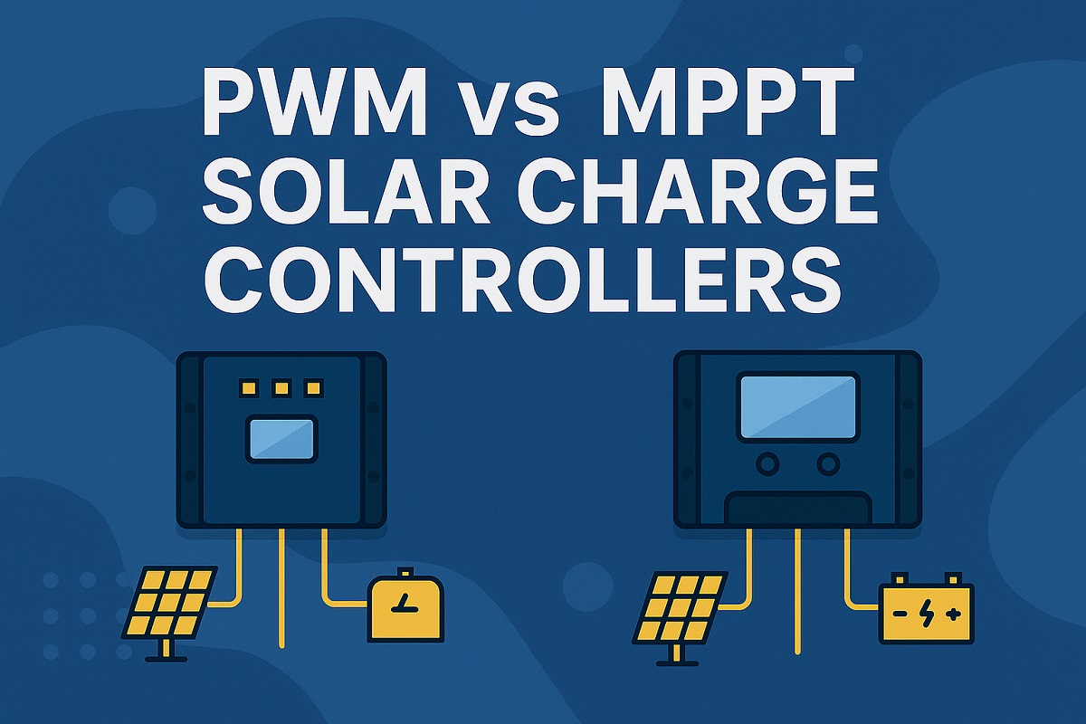 PWM vs MPPT Solar Charge Controllers: A Complete Comparison Guide
06 June 20254216
 The U.S. Semiconductor Sector Faces Workforce Challenges Amidst Surging Demand
27 November 20233790
 Inverter Introduction: Structures, Working Principles and Features
18 February 202237333
 How 10k Resistor Color Code Stacks Up Against 220 and 100k
03 September 20254631
 Semiconductor Market Expected to Surge, Driven by Rising Number of Data Centers
04 June 20242845
 Constructing Hybrid Photovoltaics from Amorphous Silicon and Hybrid Semiconductor Nanocrystals
24 October 20221604
Nexperia USA Inc.
In Stock: 51000
United States
China
Canada
Japan
Russia
Germany
United Kingdom
Singapore
Italy
Hong Kong(China)
Taiwan(China)
France
Korea
Mexico
Netherlands
Malaysia
Austria
Spain
Switzerland
Poland
Thailand
Vietnam
India
United Arab Emirates
Afghanistan
Åland Islands
Albania
Algeria
American Samoa
Andorra
Angola
Anguilla
Antigua & Barbuda
Argentina
Armenia
Aruba
Australia
Azerbaijan
Bahamas
Bahrain
Bangladesh
Barbados
Belarus
Belgium
Belize
Benin
Bermuda
Bhutan
Bolivia
Bonaire, Sint Eustatius and Saba
Bosnia & Herzegovina
Botswana
Brazil
British Indian Ocean Territory
British Virgin Islands
Brunei
Bulgaria
Burkina Faso
Burundi
Cabo Verde
Cambodia
Cameroon
Cayman Islands
Central African Republic
Chad
Chile
Christmas Island
Cocos (Keeling) Islands
Colombia
Comoros
Congo
Congo (DRC)
Cook Islands
Costa Rica
Côte d’Ivoire
Croatia
Cuba
Curaçao
Cyprus
Czechia
Denmark
Djibouti
Dominica
Dominican Republic
Ecuador
Egypt
El Salvador
Equatorial Guinea
Eritrea
Estonia
Eswatini
Ethiopia
Falkland Islands
Faroe Islands
Fiji
Finland
French Guiana
French Polynesia
Gabon
Gambia
Georgia
Ghana
Gibraltar
Greece
Greenland
Grenada
Guadeloupe
Guam
Guatemala
Guernsey
Guinea
Guinea-Bissau
Guyana
Haiti
Honduras
Hungary
Iceland
Indonesia
Iran
Iraq
Ireland
Isle of Man
Israel
Jamaica
Jersey
Jordan
Kazakhstan
Kenya
Kiribati
Kosovo
Kuwait
Kyrgyzstan
Laos
Latvia
Lebanon
Lesotho
Liberia
Libya
Liechtenstein
Lithuania
Luxembourg
Macao(China)
Madagascar
Malawi
Maldives
Mali
Malta
Marshall Islands
Martinique
Mauritania
Mauritius
Mayotte
Micronesia
Moldova
Monaco
Mongolia
Montenegro
Montserrat
Morocco
Mozambique
Myanmar
Namibia
Nauru
Nepal
New Caledonia
New Zealand
Nicaragua
Niger
Nigeria
Niue
Norfolk Island
North Korea
North Macedonia
Northern Mariana Islands
Norway
Oman
Pakistan
Palau
Palestinian Authority
Panama
Papua New Guinea
Paraguay
Peru
Philippines
Pitcairn Islands
Portugal
Puerto Rico
Qatar
Réunion
Romania
Rwanda
Samoa
San Marino
São Tomé & Príncipe
Saudi Arabia
Senegal
Serbia
Seychelles
Sierra Leone
Sint Maarten
Slovakia
Slovenia
Solomon Islands
Somalia
South Africa
South Sudan
Sri Lanka
St Helena, Ascension, Tristan da Cunha
St. Barthélemy
St. Kitts & Nevis
St. Lucia
St. Martin
St. Pierre & Miquelon
St. Vincent & Grenadines
Sudan
Suriname
Svalbard & Jan Mayen
Sweden
Syria
Tajikistan
Tanzania
Timor-Leste
Togo
Tokelau
Tonga
Trinidad & Tobago
Tunisia
Turkey
Turkmenistan
Turks & Caicos Islands
Tuvalu
U.S. Outlying Islands
U.S. Virgin Islands
Uganda
Ukraine
Uruguay
Uzbekistan
Vanuatu
Vatican City
Venezuela
Wallis & Futuna
Yemen
Zambia
Zimbabwe
![2N7002,215]() 2N7002,215
2N7002,215Nexperia USA Inc.
![2N7002P,215]() 2N7002P,215
2N7002P,215Nexperia USA Inc.
![PMZ350UPEYL]() PMZ350UPEYL
PMZ350UPEYLNexperia USA Inc.
![PSMN4R8-100BSEJ]() PSMN4R8-100BSEJ
PSMN4R8-100BSEJNexperia USA Inc.
![BSS84,215]() BSS84,215
BSS84,215Nexperia USA Inc.
![BSS138AKAR]() BSS138AKAR
BSS138AKARNexperia USA Inc.
![BUK98150-55A/CUF]() BUK98150-55A/CUF
BUK98150-55A/CUFNexperia USA Inc.
![NX3008NBKW,115]() NX3008NBKW,115
NX3008NBKW,115Nexperia USA Inc.
![BSH205G2R]() BSH205G2R
BSH205G2RNexperia USA Inc.
![PMV40UN2R]() PMV40UN2R
PMV40UN2RNexperia USA Inc.


