

 Product
 Brand
Brand Articles
 Tools
Tools
W25Q128JVSIQ 8SOIC 3V 128M-bit serial flash memory:Datasheet, Pinout ang Package


SpiFlash® Memory IC SpiFlash® Series 5.23mm mm
W25Q128JVSIQ is an integrated circuit. This article is going to introduce pinout, features, and more details about W25Q128JVSIQ.

Reliable W25Q128JVSIQ Supplier and W25Q128JVSIQ Distributor in China - Rantle East Electronic
What is the W25Q128JVSIQ?
The W25Q128JVSIQ (128M-bit) Serial Flash memory provides a storage solution for systems with limited space, pins, and power. The 25Q series offers flexibility and performance well beyond ordinary Serial Flash devices. They are ideal for code shadowing to RAM, executing code directly from Dual/Quad SPI (XIP), and storing voice, text, and data. The device operates on a single 2.7V to 3.6V power supply with current consumption as low as 1µA for power-down. All devices are offered in space-saving packages.
The W25Q128JVSIQ array is organized into 65,536 programmable pages of 256-bytes each. Up to 256 bytes can be programmed at a time. Pages can be erased in groups of 16 (4KB sector erase), groups of 128 (32KB block erase), groups of 256 (64KB block erase), or the entire chip (chip erase). The W25Q128JV has 4,096 erasable sectors and 256 erasable blocks respectively. The small 4KB sectors allow for greater flexibility in applications that require data and parameter storage. (See Figure 2.)
The W25Q128JVSIQ supports the standard Serial Peripheral Interface (SPI), Dual/Quad I/O SPI: Serial Clock, Chip Select, Serial Data I/O0 (DI), I/O1 (DO), I/O2, and I/O3. SPI clock frequencies of W25Q128JVSIQ of up to 133MHz are supported allowing equivalent clock rates of 266MHz (133MHz x 2) for Dual I/O and 532MHz (133MHz x 4) for Quad I/O when using the Fast Read Dual/Quad I/O. These transfer rates can outperform standard Asynchronous 8 and 16-bit Parallel Flash memories.
W25Q128JVSIQ Features
New Family of SpiFlash Memories
– W25Q128JV: 128M-bit / 16M-byte
– Standard SPI: CLK, /CS, DI, DO
– Dual SPI: CLK, /CS, IO0, IO1
– Quad SPI: CLK, /CS, IO0, IO1, IO2, IO3
– Software & Hardware Reset(1)
Highest Performance Serial Flash
– 133MHz Single, Dual/Quad SPI clocks
– 266/532MHz equivalent Dual/Quad SPI
– 66MB/S continuous data transfer rate
– Min. 100K Program-Erase cycles per sector
– More than 20-year data retention
Efficient “Continuous Read”
– Continuous Read with 8/16/32/64-Byte Wrap
– As few as 8 clocks to address memory
– Allows true XIP (execute in place) operation
Low Power, Wide Temperature Range
– Single 2.7 to 3.6V supply
– <1µA Power-down (type.)
– -40°C to +85°C operating range
– -40°C to +105°C operating range
Flexible Architecture with 4KB sectors
– Uniform Sector/Block Erase (4K/32K/64K-Byte)
– Program 1 to 256 bytes per programmable page
– Erase/Program Suspend & Resume
Advanced Security Features
– Software and Hardware Write-Protect
– Power Supply Lock-Down
– Special OTP protection
– Top/Bottom, Complement array protection
– Individual Block/Sector array protection
– 64-Bit Unique ID for each device
– Discoverable Parameters (SFDP) Register
– 3X256-Bytes Security Registers with OTP locks
– Volatile & Non-volatile Status Register Bits
Space Efficient Packaging
– 8-pin SOIC 208-mil
– 16-pin SOIC 300-mil (additional /RESET pin)
– 8-pad WSON 6x5-mm / 8x6-mm
– 24-ball TFBGA 8x6-mm (6x4/5x5 ball array)
– 24-ball WLCSP
– Contact Winbond for KGD and other options
Specifications
- TypeParameter
- Factory Lead Time10 Weeks
- Mounting Type
The "Mounting Type" in electronic components refers to the method used to attach or connect a component to a circuit board or other substrate, such as through-hole, surface-mount, or panel mount.
Surface Mount - Package / Case
refers to the protective housing that encases an electronic component, providing mechanical support, electrical connections, and thermal management.
8-SOIC (0.209, 5.30mm Width) - Surface Mount
having leads that are designed to be soldered on the side of a circuit board that the body of the component is mounted on.
YES - Memory TypesNon-Volatile
- Operating Temperature
The operating temperature is the range of ambient temperature within which a power supply, or any other electrical equipment, operate in. This ranges from a minimum operating temperature, to a peak or maximum operating temperature, outside which, the power supply may fail.
-40°C~85°C TA - Packaging
Semiconductor package is a carrier / shell used to contain and cover one or more semiconductor components or integrated circuits. The material of the shell can be metal, plastic, glass or ceramic.
Tray - Series
In electronic components, the "Series" refers to a group of products that share similar characteristics, designs, or functionalities, often produced by the same manufacturer. These components within a series typically have common specifications but may vary in terms of voltage, power, or packaging to meet different application needs. The series name helps identify and differentiate between various product lines within a manufacturer's catalog.
SpiFlash® - Published2012
- Pbfree Code
The "Pbfree Code" parameter in electronic components refers to the code or marking used to indicate that the component is lead-free. Lead (Pb) is a toxic substance that has been widely used in electronic components for many years, but due to environmental concerns, there has been a shift towards lead-free alternatives. The Pbfree Code helps manufacturers and users easily identify components that do not contain lead, ensuring compliance with regulations and promoting environmentally friendly practices. It is important to pay attention to the Pbfree Code when selecting electronic components to ensure they meet the necessary requirements for lead-free applications.
yes - Part Status
Parts can have many statuses as they progress through the configuration, analysis, review, and approval stages.
Active - Moisture Sensitivity Level (MSL)
Moisture Sensitivity Level (MSL) is a standardized rating that indicates the susceptibility of electronic components, particularly semiconductors, to moisture-induced damage during storage and the soldering process, defining the allowable exposure time to ambient conditions before they require special handling or baking to prevent failures
3 (168 Hours) - Number of Terminations8
- ECCN Code
An ECCN (Export Control Classification Number) is an alphanumeric code used by the U.S. Bureau of Industry and Security to identify and categorize electronic components and other dual-use items that may require an export license based on their technical characteristics and potential for military use.
3A991.B.1.A - Additional Feature
Any Feature, including a modified Existing Feature, that is not an Existing Feature.
IT ALSO OPERATES AT 104 MHZ CLOCK FREQUENCY AT 2.7 TO 3.0 V SUPPLY VOLTAGE - HTS Code
HTS (Harmonized Tariff Schedule) codes are product classification codes between 8-1 digits. The first six digits are an HS code, and the countries of import assign the subsequent digits to provide additional classification. U.S. HTS codes are 1 digits and are administered by the U.S. International Trade Commission.
8542.32.00.51 - Voltage - Supply
Voltage - Supply refers to the range of voltage levels that an electronic component or circuit is designed to operate with. It indicates the minimum and maximum supply voltage that can be applied for the device to function properly. Providing supply voltages outside this range can lead to malfunction, damage, or reduced performance. This parameter is critical for ensuring compatibility between different components in a circuit.
3.3V - Terminal Position
In electronic components, the term "Terminal Position" refers to the physical location of the connection points on the component where external electrical connections can be made. These connection points, known as terminals, are typically used to attach wires, leads, or other components to the main body of the electronic component. The terminal position is important for ensuring proper connectivity and functionality of the component within a circuit. It is often specified in technical datasheets or component specifications to help designers and engineers understand how to properly integrate the component into their circuit designs.
DUAL - Peak Reflow Temperature (Cel)
Peak Reflow Temperature (Cel) is a parameter that specifies the maximum temperature at which an electronic component can be exposed during the reflow soldering process. Reflow soldering is a common method used to attach electronic components to a circuit board. The Peak Reflow Temperature is crucial because it ensures that the component is not damaged or degraded during the soldering process. Exceeding the specified Peak Reflow Temperature can lead to issues such as component failure, reduced performance, or even permanent damage to the component. It is important for manufacturers and assemblers to adhere to the recommended Peak Reflow Temperature to ensure the reliability and functionality of the electronic components.
NOT SPECIFIED - Number of Functions1
- Terminal Pitch
The center distance from one pole to the next.
1.27mm - Time@Peak Reflow Temperature-Max (s)
Time@Peak Reflow Temperature-Max (s) refers to the maximum duration that an electronic component can be exposed to the peak reflow temperature during the soldering process, which is crucial for ensuring reliable solder joint formation without damaging the component.
NOT SPECIFIED - JESD-30 Code
JESD-30 Code refers to a standardized descriptive designation system established by JEDEC for semiconductor-device packages. This system provides a systematic method for generating designators that convey essential information about the package's physical characteristics, such as size and shape, which aids in component identification and selection. By using JESD-30 codes, manufacturers and engineers can ensure consistency and clarity in the specification of semiconductor packages across various applications and industries.
S-PDSO-G8 - Interface
In electronic components, the term "Interface" refers to the point at which two different systems, devices, or components connect and interact with each other. It can involve physical connections such as ports, connectors, or cables, as well as communication protocols and standards that facilitate the exchange of data or signals between the connected entities. The interface serves as a bridge that enables seamless communication and interoperability between different parts of a system or between different systems altogether. Designing a reliable and efficient interface is crucial in ensuring proper functionality and performance of electronic components and systems.
SPI - Memory Size
The memory capacity is the amount of data a device can store at any given time in its memory.
128Mb 16M x 8 - Operating Mode
A phase of operation during the operation and maintenance stages of the life cycle of a facility.
SYNCHRONOUS - Clock Frequency
Clock frequency, also known as clock speed, refers to the rate at which a processor or electronic component can execute instructions. It is measured in hertz (Hz) and represents the number of cycles per second that the component can perform. A higher clock frequency typically indicates a faster processing speed and better performance. However, it is important to note that other factors such as architecture, efficiency, and workload also play a significant role in determining the overall performance of a component. In summary, clock frequency is a crucial parameter that influences the speed and efficiency of electronic components in processing data and executing tasks.
133MHz - Memory Format
Memory Format in electronic components refers to the specific organization and structure of data storage within a memory device. It defines how data is stored, accessed, and managed within the memory module. Different memory formats include RAM (Random Access Memory), ROM (Read-Only Memory), and various types of flash memory. The memory format determines the speed, capacity, and functionality of the memory device, and it is crucial for compatibility with other components in a system. Understanding the memory format is essential for selecting the right memory module for a particular application or device.
FLASH - Memory Interface
An external memory interface is a bus protocol for communication from an integrated circuit, such as a microprocessor, to an external memory device located on a circuit board.
SPI - Quad I/O, QPI, DTR - Organization
In the context of electronic components, the parameter "Organization" typically refers to the arrangement or structure of the internal components within a device or system. It can describe how various elements such as transistors, resistors, capacitors, and other components are physically arranged and interconnected on a circuit board or within a semiconductor chip.The organization of electronic components plays a crucial role in determining the functionality, performance, and efficiency of a device. It can impact factors such as signal propagation, power consumption, thermal management, and overall system complexity. Engineers carefully design the organization of components to optimize the operation of electronic devices and ensure reliable performance.Different types of electronic components may have specific organizational requirements based on the intended application and design considerations. For example, integrated circuits may have a highly compact and intricate organization to maximize functionality within a small footprint, while larger electronic systems may have a more modular and distributed organization to facilitate maintenance and scalability.
16MX8 - Memory Width
Memory width refers to the number of bits that can be read or written to memory at one time. It is an important specification in electronic components, particularly in memory devices like RAM and cache. A wider memory width allows for greater data throughput, enabling faster performance as more data can be processed simultaneously. Memory width can vary among different types of memory and can impact both the complexity and efficiency of data handling within electronic systems.
8 - Write Cycle Time - Word, Page
Write Cycle Time - Word, Page refers to the duration required to write data to a specific memory cell or a page of memory in electronic components, particularly in non-volatile memories like Flash or EEPROM. It indicates the time taken to complete a writing operation for a single word or an entire page of data. This parameter is crucial for determining the performance and speed of memory devices in applications where quick data storage is essential. It impacts the overall efficiency in data handling, affecting both read and write speeds in memory-related operations.
3ms - Memory Density
Memory density in electronic components refers to the amount of data that can be stored in a given physical space or memory module. It is typically measured in bits or bytes per unit area, such as bits per square inch. Higher memory density means that more data can be stored in a smaller space, which is important for devices with limited physical size or power constraints. Memory density is a key factor in determining the capacity and performance of memory devices, such as RAM, ROM, and flash memory, and is a critical consideration in the design and manufacturing of electronic products.
134217728 bit - Parallel/Serial
The parameter "Parallel/Serial" in electronic components refers to the method of data transmission or communication within the component. In parallel communication, multiple bits of data are transmitted simultaneously over multiple channels or wires. This allows for faster data transfer rates but requires more physical connections and can be more susceptible to signal interference.On the other hand, in serial communication, data is transmitted sequentially over a single channel or wire. While serial communication may have slower data transfer rates compared to parallel communication, it is more cost-effective, requires fewer connections, and is less prone to signal interference.The choice between parallel and serial communication depends on the specific requirements of the electronic component and the overall system design, balancing factors such as speed, cost, complexity, and reliability.
SERIAL - Programming Voltage
A special high-voltage supply that supplies the potential and energy for altering the state of certain nonvolatile memory arrays. On some devices, the presence of VPP also acts as a program enable signal (P).
3V - Alternate Memory Width
Alternate Memory Width is a parameter in electronic components that refers to the ability of a memory device to operate with different data bus widths. This means that the memory device can support various configurations of data bus widths, allowing for flexibility in system design and compatibility with different applications. By offering alternate memory widths, the device can be used in a wider range of systems without requiring significant changes to the overall design. This parameter is important for optimizing performance and efficiency in electronic systems by providing options for data transfer and storage based on specific requirements.
1 - Voltage - Supply (Max)
Voltage - Supply (Max) is a parameter in electronic components that specifies the maximum voltage that can be safely applied to the component for proper operation. This parameter is crucial for ensuring the component's longevity and preventing damage due to overvoltage conditions. Exceeding the maximum supply voltage can lead to component failure, reduced performance, or even permanent damage. Designers must carefully consider this parameter when selecting components and designing circuits to ensure reliable and safe operation within the specified voltage limits.
3.6V - Voltage - Supply (Min)
Voltage - Supply (Min) is a parameter in electronic components that specifies the minimum voltage required for the component to operate within its specified performance range. This parameter indicates the lowest voltage level that can be safely applied to the component without causing malfunctions or damage. It is crucial to ensure that the supply voltage provided to the component is equal to or higher than the specified minimum voltage to guarantee proper functionality and reliability. Failure to meet this requirement may result in erratic behavior, reduced performance, or even permanent damage to the component.
3V - Ambient Temperature Range High
This varies from person to person, but it is somewhere between 68 and 77 degrees F on average. The temperature setting that is comfortable for an individual may fluctuate with humidity and outside temperature as well. The temperature of an air conditioned room can also be considered ambient temperature.
85°C - Height2.16mm
- Length5.23mm
- Width5.23mm
- RoHS Status
RoHS means “Restriction of Certain Hazardous Substances” in the “Hazardous Substances Directive” in electrical and electronic equipment.
ROHS3 Compliant
W25Q128JVSIQ Pinout
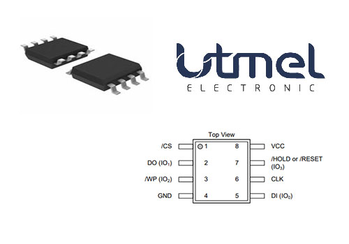
W25Q128JVSIQ Pinout
W25Q128JVSIQ CAD Model
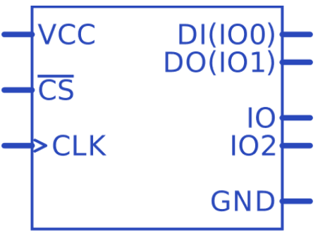
W25Q128JVSIQ Symbol
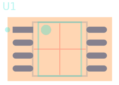
W25Q128JVSIQ Footprint
W25Q128JVSIQ Block Diagram
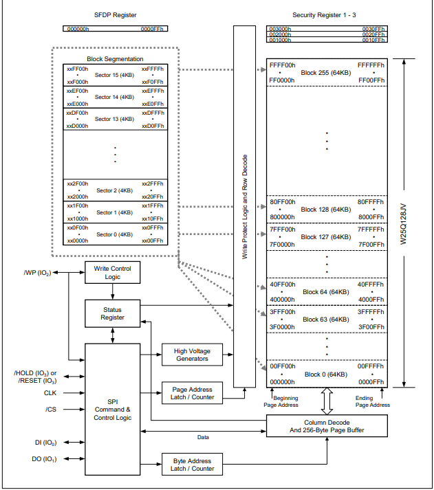
W25Q128JVSIQ Block Diagram
W25Q128JVSIQ Functional description
Standard SPI Instructions
Dual SPI Instructions
Quad SPI Instructions
Software Reset & Hardware /RESET pin
W25Q128JVSIQ Package Information

8-Pin SOIC
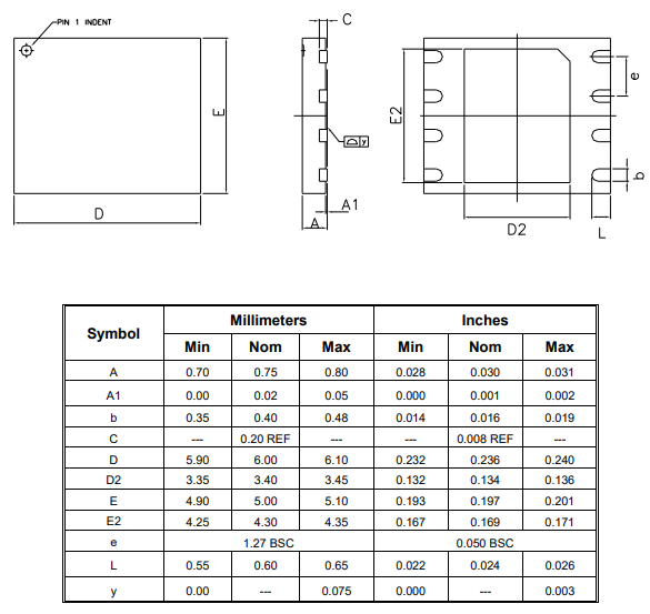
8-Pad WSON 6x5-mm
W25Q128JVSIQ Manufacturer
Winbond Electronics Corporation is a memory IC company engaged in design, manufacturing, and sales service to provide its global customers top quality memory solutions. Winbond’s product lines include Code Storage Flash Memory, Serial and Parallel NAND, Specialty DRAM, and Mobile DRAM. Winbond products are widely used by companies in the IoT vertical markets such as computing, connected multimedia devices, automobile, networking systems, and industrial. Winbond offers automotive and Industrial –Plus grade Flash and DRAM products with longevity support. Winbond has approximately 2,200 employees worldwide, which includes a 12-inch FAB at its headquarters in Taichung, Taiwan.
Datasheet PDF
- Datasheets :
- PCN Packaging :
Popularity by Region
Parts with Similar Specs
- ImagePart NumberManufacturerPackage / CaseInterfaceSupply VoltageNumber of TerminationsTerminal PitchOperating ModeNumber of FunctionsTerminal PositionView Compare
![W25Q128JVSIQ]()
W25Q128JVSIQ
8-SOIC (0.209, 5.30mm Width)
SPI
3.3 V
8
1.27 mm
SYNCHRONOUS
1
DUAL
![MX25U1635FM2I-10G]()
8-SOIC (0.209, 5.30mm Width)
SPI, Serial
1.8 V
8
1.27 mm
SYNCHRONOUS
1
DUAL
![MX25L512EMI-10G]()
SOIC
SPI, Serial
3 V
8
1.27 mm
SYNCHRONOUS
1
DUAL
![SST26VF016B-104I/SN]()
8-SOIC (0.154, 3.90mm Width)
SPI
3 V
8
1.27 mm
SYNCHRONOUS
1
DUAL
![MX25U6435FM2I-10G]()
SOIC
SPI, Serial
1.8 V
8
1.27 mm
SYNCHRONOUS
1
DUAL


What’s the needed note of W25Q128JVSIQ?
IO0 and IO1 are used for Standard and Dual SPI instructions.
How many pins of W25Q128JVSIQ ?
8 pins.
 PCF8574A Expander: Datasheet, Pinout, Comparison
20 August 20212501
 Microchip PIC16F1613TIML Microcontroller Datasheet Overview
29 February 2024176
 ADG1408 Multiplexer: Datasheet, Circuit and Price
12 November 20214372
 FLIRE5 Infrared Cameras: Datasheet, Price and Benefits
03 August 20211497
 PCA9555PW Expander: Features, Applications and Datasheet
02 November 2023582
 TDA2005 Amplifier: Pinout, Datasheet, Circuit
12 July 202116433
 SN74LVC1G14DCKR: Overview, Features, and Applications
13 December 2023966
 TMP100 VS TMP101
12 July 20212267
 Google Acquires MicroLED Display Company Raxium, May Boost Its AR Headset
09 May 20222438
 Texas Semiconductor Summit: A Step Towards Overcoming Chip Shortage
14 October 20232960
 Devices based on Semiconductor Laser Chaos for Optical Communications
22 February 20232473
 What JEDEC JEP203 and JEP204 Actually Change for SiC Qualification Engineers and Component Buyers
29 July 2026506
 What is a Reed Relay?
16 April 20219637
 C1815 vs C945 Key Features and Application Guide
01 September 20254399
 What is a Multimeter?
20 December 20217072
 Humidity Sensor: Classification, Package and Application
13 November 20255699
Winbond Electronics
In Stock: 5565
Minimum: 1 Multiples: 1
Qty
Unit Price
Ext Price
1
$1.852664
$1.85
10
$1.747796
$17.48
100
$1.648864
$164.89
500
$1.555532
$777.77
1000
$1.467483
$1,467.48
Not the price you want? Send RFQ Now and we'll contact you ASAP.
Inquire for More Quantity
![W25Q80DVSSIG]() W25Q80DVSSIG
W25Q80DVSSIGWinbond Electronics
![W9825G6KH-6]() W9825G6KH-6
W9825G6KH-6Winbond Electronics
![W27C512-45Z]() W27C512-45Z
W27C512-45ZWinbond Electronics
![W25Q32JWBYIQ TR]() W25Q32JWBYIQ TR
W25Q32JWBYIQ TRWinbond Electronics
![W9812G6KH-6]() W9812G6KH-6
W9812G6KH-6Winbond Electronics
![W25Q64FVSSIG]() W25Q64FVSSIG
W25Q64FVSSIGWinbond Electronics
![W25Q64JVSSIQ]() W25Q64JVSSIQ
W25Q64JVSSIQWinbond Electronics
![W25X40CLSNIG]() W25X40CLSNIG
W25X40CLSNIGWinbond Electronics
![W25Q128FVSIG]() W25Q128FVSIG
W25Q128FVSIGWinbond Electronics

