

 Product
 Brand
Brand Articles
 Tools
Tools
Sourcing GaN Power Devices for AI Servers, EVs, and Industrial Applications
Quick Answer Summary:
GaN power devices are wide-bandgap semiconductors that offer superior electron mobility and sub-nanosecond switching speeds compared to legacy Silicon. In high-power, high-density applications like 100kW+ AI server racks and 800V electric vehicles (EVs), GaN is critical for reducing footprint and power losses. However, securing reliable GaN inventory requires navigating multi-month lead times, complex gate-drive requirements, and strict reliability standards.
The Procurement Decision Framework
For high-tech procurement officers, sourcing GaN power devices is not a simple transactional task. It requires balancing strict engineering requirements—such as thermal limits, gate-drive compatibility, and dynamic on-resistance—with volatile supply chain realities, including packaging availability, shifting foundry landscapes, and trade compliance.
Sourcing GaN Power Devices: The Procurement Decision Framework
Engineering Validation
• Gate-Drive Compatibility
• Dynamic RDS(on) Limits
• Thermal Isolation Design
• Standard Packaging (DFN)
↓
Supply Chain Resilience
• Dual-Sourcing Strategy
• Upstream Substrate Tracking
• Independent Distribution
• AS6081-Certified Testing
The GaN Revolution: Powering 100kW+ AI Racks and 800V EVs
Gallium Nitride (GaN) High-Electron-Mobility Transistors (HEMTs) have officially graduated from consumer fast-charging adapters into high-reliability, high-power industrial and automotive environments. This transition is driven by GaN's fundamental physics advantages over legacy Silicon (Si). With a bandgap of 3.4 eV (compared to Silicon's 1.1 eV), GaN devices can withstand higher electric fields, enabling much thinner drift regions and low on-resistance.
Key Specifications to Compare
When evaluating GaN power devices against legacy Silicon, procurement and engineering teams must focus on several critical performance metrics:
Figure of Merit (FoM): Calculated as Gate Charge ($Q_g$) multiplied by On-Resistance ($R_{DS(on)}$), FoM measures a transistor's efficiency. Silicon transistors typically exhibit an FoM of approximately 72, whereas advanced GaN transistors are typically reported to achieve an FoM of around 1. This nearly 100-fold improvement means GaN is significantly more "on" when conducting and vastly faster at transitioning between states.
Vampire Power (No-Load Losses): In massive data center environments, idle power consumption scales rapidly. Standard Silicon power supplies can draw up to approximately 1.2W at idle, whereas comparable GaN-based designs can reduce this "vampire power" to as low as 110mW—a potential 90% reduction in wasted energy, depending on design.
Planar vs. Wire-Wound Transformers: High-frequency GaN designs often replace bulky, hand-wound copper wire transformers with planar transformers. These are dedicated mini-PCBs where copper traces act as the windings, sandwiched between ferrite cores. This design eliminates manufacturing inconsistencies and minimizes stray inductance.
Synchronous Rectification: The efficiency jump in GaN-based systems is further enhanced by pairing GaN switches with active/synchronous rectification on the output stage. Replacing traditional output diodes (which can lose over 2W in heat) with secondary MOSFETs (reducing loss to ~0.16W) yields massive energy savings.
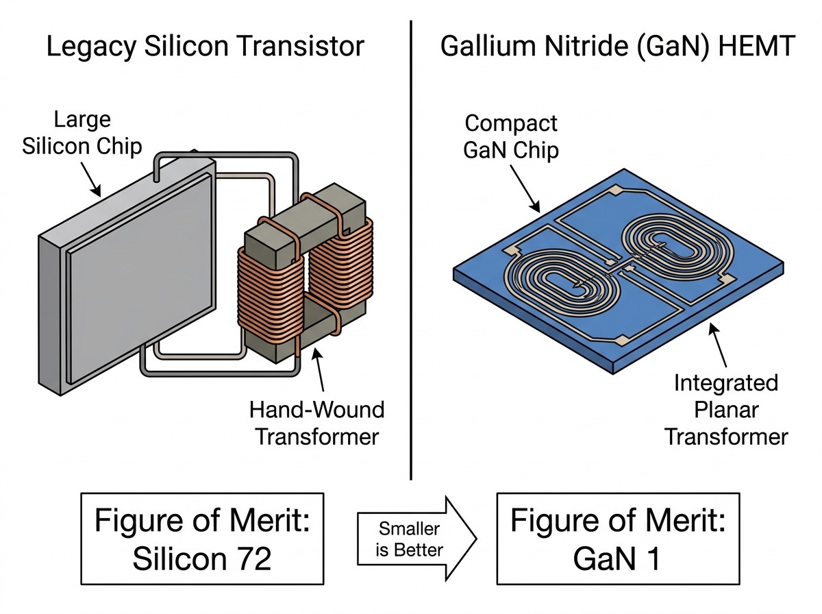
Application Boundaries: GaN vs. SiC
While both GaN and Silicon Carbide (SiC) are wide-bandgap materials, they serve different application boundaries:
| Feature / Technology | Silicon (Si) | Gallium Nitride (GaN) | Silicon Carbide (SiC) |
|---|---|---|---|
| Optimal Voltage Range | < 100V | 100V – 900V | 650V – 3.3kV+ |
| Switching Speed | Slow (Microseconds) | Ultra-Fast (Sub-nanosecond) | Medium-Fast |
| Best Use Cases | Low-cost, low-power legacy systems | AI Server PSUs, 800V OBCs, eVTOL, LiDAR | EV Traction Inverters, Grid Infrastructure |
| Thermal Conductivity | Moderate | Moderate | High |
In AI data centers, power demands are surging. AI training clusters routinely exceed 130 kW per rack, with advanced liquid-cooled setups surpassing 250 kW. To support these densities, power supply units (PSUs) must transition from 12V to 48V distribution architectures. Optimized GaN half-bridge modules designed for these 800VDC architectures can achieve up to 98.7% peak efficiency and 97.5% efficiency at full load, as reported in manufacturer datasheets, allowing engineers to shrink passive components like inductors and EMI filters.
Architectural Reliability Challenges: Thermal, Gate-Drive, and Dynamic RDS(on)
A common misconception among procurement departments is that GaN HEMTs are simple "drop-in" replacements for Silicon MOSFETs. In reality, GaN devices require entirely different gate-drive circuitry and PCB layouts to prevent catastrophic field failures.
Everything is Better: GaN vs Silicon Power Supplies
Technical Breakdown of Engineering Risks
1. Dynamic RDS(on) (Drain Current Collapse)
Under high drain voltage stress, electrons can become trapped in the active region of the GaN HEMT structure. This charge trapping causes a transient, recoverable increase in on-resistance, known as dynamic RDS(on). If unmitigated by proper device passivation, this phenomenon leads to unexpected conduction losses, thermal runaway, and eventual system failure.
2. Parasitic Inductance
Because GaN switches at sub-nanosecond speeds, even nanohenries of stray layout inductance can cause destructive voltage overshoots. To mitigate this, designs must utilize an array of Surface Mount (SMD) Multi-Layer Ceramic Capacitors (MLCCs) placed millimeters from the GaN transistor's pins to keep trace inductance near zero.
3. Thermal Contamination
High-density layouts are highly prone to thermal contamination. For example, heat generated by a primary component's heatsink can degrade nearby components if they are not thermally isolated. Furthermore, standard electrolytic capacitors degrade quickly under high heat and ripple currents. To survive, GaN boards utilize advanced Solid Polymer capacitors, which do not evaporate and can safely operate closer to their rated limits (e.g., using a 16V-rated polymer capacitor on a 12V line, rather than heavily derating to a bulky 35V electrolytic capacitor).
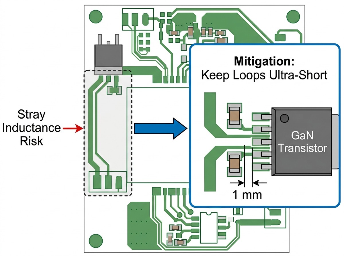
Stray Inductance Risk in GaN Layouts
Sub-nanosecond Switching Speed (GaN)
↓
Generates high di/dt
Stray Trace Inductance
Even a few nanohenries can matter
↓
Causes voltage spikes
Destructive Voltage Overshoots
Mitigation: Place SMD MLCCs only a few millimeters from the GaN device pins to minimize the high-current switching loop.
Reliability Testing and Verification
To ensure long-term reliability in harsh environments, procurement must verify that GaN devices are qualified beyond standard silicon AEC-Q101 stress testing. Buyers should mandate compliance with GaN-specific JEDEC guidelines established by the JC-70 committee, specifically:
JEP-173: Standard Test Method for Evaluation of Dynamic ON-Resistance of GaN Power Transistors.
JEP-180: Guideline for Switching Reliability Evaluation Procedures for Gallium Nitride Power Conversion Devices.
4 Strategic Procurement Solutions for GaN Power Devices
Amidst ongoing passive and power semiconductor supply tightness, procurement officers must move away from reactive buying and implement a structured sourcing playbook.
1. Qualify Pin-to-Pin Alternatives Early
Do not wait for a primary component to hit absolute zero stock before looking for alternatives. Work with engineering teams to pre-qualify alternative GaN dies from different manufacturers. Ensure that the gate-drive requirements, threshold voltages, and thermal characteristics are aligned so that alternative parts can be approved on the Active Vendor List (AVL).
2. Prioritize Standard Packaging
While highly integrated, custom GaN modules offer excellent power density, they introduce severe supply chain single-source risks. Opting for standard, widely produced surface-mount packages—such as TOLL (TO-Leadless), DFN, or PQFN—yields a much broader pool of available stock.
However, standard packages face thermomechanical wear-out challenges, such as Coefficient of Thermal Expansion (CTE) mismatches that cause solder-joint cracking. To mitigate this, prioritize the emerging engineering trend toward double-side cooling ceramic QFN/DFN architectures, which offer superior thermal dissipation without requiring custom footprints.
3. Monitor Upstream Substrate Supply
GaN-on-Silicon and GaN-on-SiC devices rely on complex upstream supply chains. Shifting foundry landscapes, raw material bottlenecks, and trade compliance volatility serve as leading indicators of finished-good shortages. Establish relationships with suppliers who maintain diversified wafer-fab and packaging locations to mitigate regional supply disruptions.
4. Leverage Independent Stocking Networks
When franchised distributors quote extensive, multi-month lead times, independent stocking networks become essential. These distributors can tap into global excess inventory, OEM surplus, and unallocated factory stock to keep production lines running.
Bypassing Supply Tightness: Partnering with UTMEL Electronics
Sourcing wide-bandgap semiconductors from the open market requires rigorous quality control to avoid counterfeit, mismarked, or poorly stored components. Procurement teams must partner with distributors who mandate AS6081-certified laboratory testing, visual inspection, and complete Certificates of Conformance (CoC).
UTMEL Electronics serves as a strategic partner for high-tech procurement officers navigating these supply challenges. In the current market, lead times for wide-bandgap GaN devices from Tier-1 suppliers (such as Infineon's CoolGaN and Navitas's GaNFast) typically stretch between 12 to 24 weeks, according to industry sourcing reports due to the rapid deployment of 800VDC AI server racks and EV platforms. UTMEL helps bypass these factory lead times by providing access to an extensive global inventory of advanced GaN power switches, driver ICs, and high-speed converters.
To understand how these technologies are reshaping the power landscape, read our analysis on how SiC and GaN power devices are redefining AI data centers and 800V EVs. Additionally, keeping track of power management ICs trends, AI demand, and supply risks is essential for proactive planning. For a broader view of the market, consult our power semiconductors shortage outlook, supply lead times, and sourcing options.
Datasheet & Verification Checklist for GaN Procurement
Before issuing a Purchase Order (PO) for alternate GaN power devices, review this checklist with your engineering team:
[ ] Footprint & Package Compatibility: Is the alternate part a true physical match (e.g., TOLL, DFN, PQFN)?
[ ] Gate-Drive Voltage Limits: Does the alternate part's gate threshold voltage ($V_{GS(th)}$) match the existing gate driver's output limits? (GaN gates are highly sensitive to overvoltage).
[ ] Dynamic RDS(on) Verification: Has the manufacturer qualified the device under JEDEC JEP-173 guidelines to ensure minimal resistance degradation under high-voltage stress?
[ ] Thermal Dissipation Path: Does the alternate part utilize top-side, bottom-side, or double-sided cooling, and does this align with the system's heatsink design?
[ ] Quality & Traceability: Does the distributor provide AS6081-certified testing and a verified Certificate of Conformance (CoC) to prevent counterfeit risks?
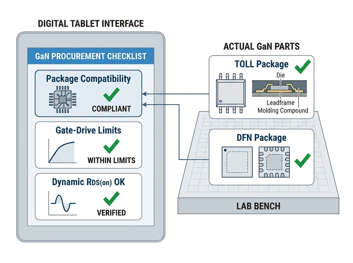
Frequently Asked Questions (FAQ)
What are GaN power devices?
GaN power devices are wide-bandgap semiconductors made from Gallium Nitride. They are primarily used as High-Electron-Mobility Transistors (HEMTs) to switch electrical power highly efficiently at high frequencies, far exceeding the performance limits of traditional Silicon.
How do GaN devices power AI servers?
In AI servers, GaN devices are used in the Power Supply Units (PSUs) and Intermediate Bus Converters (IBCs) to step down voltage (such as 48V to 12V) at high frequencies. This allows for smaller passive components, reduces idle power losses, and enables the high power densities required by 100kW+ server racks.
Why are GaN power devices facing supply chain shortages?
The rapid adoption of GaN in high-power applications—such as AI data centers, 800V EV onboard chargers, and industrial power systems—has outpaced manufacturing capacity. This surge in demand, combined with shifting foundry landscapes and raw material bottlenecks, has stretched lead times to 12 to 24 weeks.
Can I replace a Silicon MOSFET directly with a GaN HEMT?
No. GaN HEMTs require specialized gate drivers capable of handling sub-nanosecond switching speeds and precise gate voltages. They also require low-inductance PCB layouts and advanced thermal management to prevent voltage spikes and thermal runaway.
What is JEDEC JEP-173?
JEP-173 is a JEDEC publication that establishes standard testing methodologies for evaluating the transient or dynamic on-resistance of GaN power transistors to verify that they do not undergo catastrophic current collapse under high-voltage switching operations.
Sources and references used for this guide
High voltage GaN HEMTs with low on-resistance for power switching applications
Source type: research source
Used for: Technical context on device design, breakdown voltage, and low on-resistance.
Caution: Foundational academic thesis; do not use for current commercial availability.Scaling AI Data Center Power Delivery with Si SiC and GaN
Source type: official company documentation
Used for: Context on designing dense, efficient, and thermally optimized PSUs for AI data centers.
Caution: Vendor whitepaper; use for architectural concepts, not neutral ranking.
 UTMEL
UTMEL
We are the professional distributor of electronic components, providing a large variety of products to save you a lot of time, effort, and cost with our efficient self-customized service. careful order preparation fast delivery service
 MOSFET vs IGBT: Structure, Switching Behavior, and How to ChooseUTMEL21 September 202624573
With the rise of new energy in recent years, the market demand for MOSFETs and IGBTs is increasing steeply. Generally used as switching devices, they are widely used in electronic circuits. MOSFETs and IGBTs are relatively similar in appearance and characteristics parameters. So what is the difference between MOSFETs and IGBTs?
Read More Introduction to FinFETUTMEL18 March 202131317
The full name of FinFET is Fin Field-Effect Transistor. It is a new complementary metal oxide semiconductor transistor. The FinFET name is based on the similarity between the shape of the transistor and the fin.
Read More What Is a MOSFET? Working Principle, Types, and Selection GuideUTMEL15 July 20268147
This guide walks through how a MOSFET works, how it differs from an ordinary bipolar transistor, the four standard types, the roles it plays in a circuit, and a practical, parameter-driven way to choose one. Because this topic invites a lot of numbers, the discussion stays qualitative on purpose. Any exact voltage, resistance, current, or thermal figure belongs to the specific part you are using, so treat the manufacturer datasheet as the final word on every number.
Read More NPN Transistors and PNP TransistorsUTMEL29 October 202010159
NPN and PNP are two types of transistors. Transistors are semiconductor devices made of doped p-type and n-type junctions. This article mainly introduces the differences between this two kinds of transistors, the methods of distinguishing them, and the application of them.
Read More An Overview of Bipolar TransistorsUTMEL27 August 20209421
Bipolar Transistor, full name bipolar junction transistor(BJT), is an electronic device with three terminals, made of three parts of semiconductors with different levels of doping. The charge flow in the transistor is mainly due to the diffusion and drift movement of carriers at the PN junction.
Read More
Subscribe to Utmel !
![BLM18PG330SN1D]() BLM18PG330SN1D
BLM18PG330SN1DMurata Electronics
![ENW-89847A3KF]() ENW-89847A3KF
ENW-89847A3KFPanasonic Electronic Components
![BLM03AX102SN1D]() BLM03AX102SN1D
BLM03AX102SN1DMurata Electronics
![TP88]() TP88
TP88Fluke Electronics
![1212039]() 1212039
1212039Phoenix Contact
![BLM15AG121SN1D]() BLM15AG121SN1D
BLM15AG121SN1DMurata Electronics
![01050003H]() 01050003H
01050003HLittelfuse Inc.
![7BB-12-9]() 7BB-12-9
7BB-12-9Murata Electronics
![7BB-20-6L0]() 7BB-20-6L0
7BB-20-6L0Murata Electronics
![PKMCS1818E20A0-R1]() PKMCS1818E20A0-R1
PKMCS1818E20A0-R1Murata Electronics


