
 Product
 Brand
Brand Articles
 Tools
Tools
2N2219 NPN Transistor: Datasheet, Equivalent and Pinout


Bipolar Transistors - BJT NPN Ampl/Switch
2N2219 is an NPN transistor, and this post will cover more details about 2N2219. Furthermore, there is huge range of Semiconductors, Capacitors, Resistors and ICs in stock. Welcome RFQ.

Long Range FM transmitter using four 2N2219 Transistors in Hindi
2N2219 Pinout

2N2219 Pinout
2N2219 CAD Model
Symbol

2N2219 Symbol
Footprint

2N2219 Footprint
2N2219 Description
The 2N2219 is an NPN transistor, when the base pin is held at the ground, the collector and emitter are left open (reverse biased), and when a signal is applied to the base pin, they are closed (forward-biased). The gain value hfe of 2N2219 is 50, which controls the transistor's amplification capacity.
Specifications
- TypeParameter
- Factory Lead Time8 Weeks
- Mount
In electronic components, the term "Mount" typically refers to the method or process of physically attaching or fixing a component onto a circuit board or other electronic device. This can involve soldering, adhesive bonding, or other techniques to secure the component in place. The mounting process is crucial for ensuring proper electrical connections and mechanical stability within the electronic system. Different components may have specific mounting requirements based on their size, shape, and function, and manufacturers provide guidelines for proper mounting procedures to ensure optimal performance and reliability of the electronic device.
Through Hole - Package / Case
refers to the protective housing that encases an electronic component, providing mechanical support, electrical connections, and thermal management.
TO-39 - Collector-Emitter Breakdown Voltage30V
- Collector-Emitter Saturation Voltage1.6V
- Number of Elements1
- Power Dissipation (Max)800mW
- hFEMin35
- Published2012
- JESD-609 Code
The "JESD-609 Code" in electronic components refers to a standardized marking code that indicates the lead-free solder composition and finish of electronic components for compliance with environmental regulations.
e0 - Pbfree Code
The "Pbfree Code" parameter in electronic components refers to the code or marking used to indicate that the component is lead-free. Lead (Pb) is a toxic substance that has been widely used in electronic components for many years, but due to environmental concerns, there has been a shift towards lead-free alternatives. The Pbfree Code helps manufacturers and users easily identify components that do not contain lead, ensuring compliance with regulations and promoting environmentally friendly practices. It is important to pay attention to the Pbfree Code when selecting electronic components to ensure they meet the necessary requirements for lead-free applications.
no - Part Status
Parts can have many statuses as they progress through the configuration, analysis, review, and approval stages.
Active - Number of Terminations3
- ECCN Code
An ECCN (Export Control Classification Number) is an alphanumeric code used by the U.S. Bureau of Industry and Security to identify and categorize electronic components and other dual-use items that may require an export license based on their technical characteristics and potential for military use.
EAR99 - Terminal Finish
Terminal Finish refers to the surface treatment applied to the terminals or leads of electronic components to enhance their performance and longevity. It can improve solderability, corrosion resistance, and overall reliability of the connection in electronic assemblies. Common finishes include nickel, gold, and tin, each possessing distinct properties suitable for various applications. The choice of terminal finish can significantly impact the durability and effectiveness of electronic devices.
Tin/Lead (Sn/Pb) - Max Operating Temperature
The Maximum Operating Temperature is the maximum body temperature at which the thermistor is designed to operate for extended periods of time with acceptable stability of its electrical characteristics.
150°C - Min Operating Temperature
The "Min Operating Temperature" parameter in electronic components refers to the lowest temperature at which the component is designed to operate effectively and reliably. This parameter is crucial for ensuring the proper functioning and longevity of the component, as operating below this temperature may lead to performance issues or even damage. Manufacturers specify the minimum operating temperature to provide guidance to users on the environmental conditions in which the component can safely operate. It is important to adhere to this parameter to prevent malfunctions and ensure the overall reliability of the electronic system.
-65°C - HTS Code
HTS (Harmonized Tariff Schedule) codes are product classification codes between 8-1 digits. The first six digits are an HS code, and the countries of import assign the subsequent digits to provide additional classification. U.S. HTS codes are 1 digits and are administered by the U.S. International Trade Commission.
8541.21.00.75 - Terminal Position
In electronic components, the term "Terminal Position" refers to the physical location of the connection points on the component where external electrical connections can be made. These connection points, known as terminals, are typically used to attach wires, leads, or other components to the main body of the electronic component. The terminal position is important for ensuring proper connectivity and functionality of the component within a circuit. It is often specified in technical datasheets or component specifications to help designers and engineers understand how to properly integrate the component into their circuit designs.
BOTTOM - Terminal Form
Occurring at or forming the end of a series, succession, or the like; closing; concluding.
WIRE - Peak Reflow Temperature (Cel)
Peak Reflow Temperature (Cel) is a parameter that specifies the maximum temperature at which an electronic component can be exposed during the reflow soldering process. Reflow soldering is a common method used to attach electronic components to a circuit board. The Peak Reflow Temperature is crucial because it ensures that the component is not damaged or degraded during the soldering process. Exceeding the specified Peak Reflow Temperature can lead to issues such as component failure, reduced performance, or even permanent damage to the component. It is important for manufacturers and assemblers to adhere to the recommended Peak Reflow Temperature to ensure the reliability and functionality of the electronic components.
NOT SPECIFIED - Time@Peak Reflow Temperature-Max (s)
Time@Peak Reflow Temperature-Max (s) refers to the maximum duration that an electronic component can be exposed to the peak reflow temperature during the soldering process, which is crucial for ensuring reliable solder joint formation without damaging the component.
NOT SPECIFIED - Pin Count
a count of all of the component leads (or pins)
3 - JESD-30 Code
JESD-30 Code refers to a standardized descriptive designation system established by JEDEC for semiconductor-device packages. This system provides a systematic method for generating designators that convey essential information about the package's physical characteristics, such as size and shape, which aids in component identification and selection. By using JESD-30 codes, manufacturers and engineers can ensure consistency and clarity in the specification of semiconductor packages across various applications and industries.
O-MBCY-W3 - Qualification Status
An indicator of formal certification of qualifications.
Not Qualified - Polarity
In electronic components, polarity refers to the orientation or direction in which the component must be connected in a circuit to function properly. Components such as diodes, capacitors, and LEDs have polarity markings to indicate which terminal should be connected to the positive or negative side of the circuit. Connecting a component with incorrect polarity can lead to malfunction or damage. It is important to pay attention to polarity markings and follow the manufacturer's instructions to ensure proper operation of electronic components.
NPN - Element Configuration
The distribution of electrons of an atom or molecule (or other physical structure) in atomic or molecular orbitals.
Single - Transistor Application
In the context of electronic components, the parameter "Transistor Application" refers to the specific purpose or function for which a transistor is designed and used. Transistors are semiconductor devices that can amplify or switch electronic signals and are commonly used in various electronic circuits. The application of a transistor can vary widely depending on its design and characteristics, such as whether it is intended for audio amplification, digital logic, power control, or radio frequency applications. Understanding the transistor application is important for selecting the right type of transistor for a particular circuit or system to ensure optimal performance and functionality.
SWITCHING - Gain Bandwidth Product
The gain–bandwidth product (designated as GBWP, GBW, GBP, or GB) for an amplifier is the product of the amplifier's bandwidth and the gain at which the bandwidth is measured.
250MHz - Collector Emitter Voltage (VCEO)
Collector-Emitter Voltage (VCEO) is a key parameter in electronic components, particularly in transistors. It refers to the maximum voltage that can be applied between the collector and emitter terminals of a transistor while the base terminal is open or not conducting. Exceeding this voltage limit can lead to breakdown and potential damage to the transistor. VCEO is crucial for ensuring the safe and reliable operation of the transistor within its specified limits. Designers must carefully consider VCEO when selecting transistors for a circuit to prevent overvoltage conditions that could compromise the performance and longevity of the component.
1.6V - Max Collector Current
Max Collector Current is a parameter used to specify the maximum amount of current that can safely flow through the collector terminal of a transistor or other electronic component without causing damage. It is typically expressed in units of amperes (A) and is an important consideration when designing circuits to ensure that the component operates within its safe operating limits. Exceeding the specified max collector current can lead to overheating, degradation of performance, or even permanent damage to the component. Designers must carefully consider this parameter when selecting components and designing circuits to ensure reliable and safe operation.
800mA - Transition Frequency
Transition Frequency in electronic components refers to the frequency at which a device can transition from one state to another, typically defining the upper limit of its operating frequency. It is a critical parameter in determining the speed and performance of active components like transistors and integrated circuits. This frequency is influenced by factors such as capacitance, resistance, and the inherent characteristics of the materials used in the component's construction. Understanding transition frequency is essential for optimizing circuit designs and ensuring reliable signal processing in various applications.
250MHz - Frequency - Transition
The parameter "Frequency - Transition" in electronic components refers to the maximum frequency at which a signal transition can occur within the component. It is a crucial specification for digital circuits as it determines the speed at which data can be processed and transmitted. A higher frequency transition allows for faster operation and better performance of the electronic component. It is typically measured in hertz (Hz) or megahertz (MHz) and is specified by the manufacturer to ensure proper functioning of the component within a given frequency range.
250MHz - Collector Base Voltage (VCBO)
Collector Base Voltage (VCBO) is the maximum allowable voltage that can be applied between the collector and base terminals of a bipolar junction transistor when the emitter is open. It is a critical parameter that determines the voltage rating of the transistor and helps prevent breakdown in the collector-base junction. Exceeding this voltage can lead to permanent damage or failure of the component.
60V - Emitter Base Voltage (VEBO)
Emitter Base Voltage (VEBO) is a parameter used in electronic components, particularly in transistors. It refers to the maximum voltage that can be applied between the emitter and base terminals of a transistor without causing damage to the device. Exceeding this voltage limit can lead to breakdown of the transistor and potential failure. VEBO is an important specification to consider when designing circuits to ensure the proper operation and reliability of the components. It is typically provided in the datasheet of the transistor and should be carefully observed to prevent any potential damage during operation.
5V - DC Current Gain-Min (hFE)
The parameter "DC Current Gain-Min (hFE)" in electronic components refers to the minimum value of the DC current gain of a bipolar junction transistor (BJT). It is a measure of how much the transistor amplifies the input current to produce the output current. The hFE value indicates the ratio of the output current to the input current when the transistor is operating in the active region. A higher hFE value signifies a higher current gain and better amplification capabilities of the transistor. It is an important parameter to consider when designing and analyzing transistor circuits for various electronic applications.
30 - Turn Off Time-Max (toff)
The parameter "Turn Off Time-Max (toff)" in electronic components refers to the maximum time taken for a device to switch from an ON state to an OFF state. It is a crucial specification in devices such as transistors, diodes, and other semiconductor components that control the flow of current. The turn-off time is important for determining the switching speed and efficiency of a component, as a shorter turn-off time generally indicates faster operation and reduced power losses. Designers and engineers use this parameter to ensure proper functioning and performance of electronic circuits and systems.
285ns - RoHS Status
RoHS means “Restriction of Certain Hazardous Substances” in the “Hazardous Substances Directive” in electrical and electronic equipment.
RoHS Compliant
Parts with Similar Specs
2N2219 Features
Small Signal NPN Transistor
Current Gain (hFE), typically 50 for small signal
Continuous Collector current (IC) is 800mA
Collector-Emitter voltage (VCEO) is 50 V
Collector-Base voltage (VCB0) is 75V
Emitter Base Voltage (VBE0) is 6V
Turn-on time is 40ns
Turn off time is 250ns
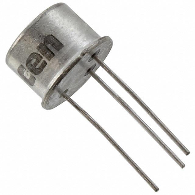
Available in To-39 Package
2N2219 Application
Driver Modules like Relay Driver, LED driver etc.
Amplifier modules like Audio amplifiers, signal Amplifiers etc.
Darlington pair
2N2219 Equivalent
2N2905
Where to use 2N2219
The 2N2219 transistor is quite similar to the 2N2222, a common NPN transistor. It does, however, come in a metal can package and can handle voltages slightly greater than a 2N2222. In general, it's just another little signal transistor found in switching and amplifying circuits.
So, if you're seeking an NPN transistor that can switch loads or provide adequate amplification, the 2N2219 could be the ideal choice for you.
How to use 2N2219
An NPN transistor, the 2N2219 is commonly employed as a switch in numerous circuits. Let's have a look at how to use one in a circuit. Because the transistor is NPN, the load to be switched should be connected to the collector and the emitter to the ground, as shown in the diagram below.

How to use 2N2219
The base resistor is another key consideration when utilizing a transistor as a switch. To limit the current flowing via the base, this resistor is connected to the transistor's base pin. We know that the transistor is a current-controlled device, which means that to turn it on, we must flow some current (IB) through the base of the transistor. The required amount of current that will be used by the load can be used to compute the value of this current. Let's say the load draws roughly 800mA at most, hence our collector current (IC) is 800mA. The value of base current IB can be computed using the formula below to make this current flow through the transistor:
IB = IC / hFE
Where hFE is the transistor's current gain, which in our case is 50. The symbol will be used to symbolize the current gain in some circumstances.
In our situation, a base current of 16mA is required to pass an 800mA collector current. We can use the equations to calculate the resistor value of the base.
RB = (VCC – VBE) / IB
Where Vcc is the load's operating voltage and VBE is the voltage between the Base and Emitter, which in our case is 1.3V according to the datasheet. As a result, the value of RB will be
RB = (12-1.3)/(16*10^-3)
= ~660 Ohms
However, because the transistor will have an inherent voltage drop across the collector current, this value will not be very accurate, so getting the maximum current from the transistor will be mostly experimental. However, this formula will yield the closest value as a starting point.
2N2219 Package


2N2219 Package
2N2219 Manufacturer
Central Semiconductor is a leading provider of superior discrete semiconductors that have been applied in electronic products all over the world since 1974. Nowadays, the company's products lines contain MOSFETs, bridge rectifiers, silicon carbide devices, protection devices, rectifiers, current limiting diodes, bipolar power transistors, standard, and custom small-signal transistors, and thyristors.
Datasheet PDF
- ReachStatement :
- Datasheets :
Popularity by Region
Is 2N2219 similar to 2N2222?
The 2N2219 transistor is very much similar to the commonly used NPN transistor 2N2222. But it comes in a metal can package and can operate on voltages slightly higher than what a 2N2222 can handle.
What is 2N2219 designed for?
It is designed for small signal general purpose and switching applications.
How does 2N2219 package?
It is available in a TO-39 package.
 TSAL6100: Datasheet, Footprint and Features
15 March 20221229
 MT8870 DTMF Receiver: Pin Description, Price and Datasheet
16 August 20214074
 LTC6951IUHF-1#PBF Clock Generator: A Comprehensive Technical Overview
06 March 2024299
 How STM32G070KBT6 Enhances Embedded Applications
24 July 2025175
 AD8361 2.5 GHz RF Power Detector: Precision Datasheet, Pinout, and Implementation Analysis
18 March 2026133
 CR2430 vs CR2450: Is there any differences between them?
24 April 202270459
 BNO080 Sensor: Datasheet, Pinout and Circuit
05 August 20215783
 TPS72325DBVR: Regulator, Pinout, Equivalent, Circuit
25 March 2022826
 Impact of IoT and WSN Integration on Productivity and Sustainability
05 March 20242457
 EMI Filter: Introduction, Functions and Applications
23 December 202012990
 Introduction to the Types of SDRAM
13 July 202113463
 Introduction to buck, boost, and buck-boost converters
28 September 202123978
 What is a USB Flash Drive?
25 May 20213270
 Battery Management System (BMS) Implementation Form and Chip Performance Analysis
28 April 20223834
 Semiconductor Cleaning: Processes, Methods and Reasons
20 April 202218894
 What is a Transmitter?
12 October 20215587
Central Semiconductor
In Stock: 85
United States
China
Canada
Japan
Russia
Germany
United Kingdom
Singapore
Italy
Hong Kong(China)
Taiwan(China)
France
Korea
Mexico
Netherlands
Malaysia
Austria
Spain
Switzerland
Poland
Thailand
Vietnam
India
United Arab Emirates
Afghanistan
Åland Islands
Albania
Algeria
American Samoa
Andorra
Angola
Anguilla
Antigua & Barbuda
Argentina
Armenia
Aruba
Australia
Azerbaijan
Bahamas
Bahrain
Bangladesh
Barbados
Belarus
Belgium
Belize
Benin
Bermuda
Bhutan
Bolivia
Bonaire, Sint Eustatius and Saba
Bosnia & Herzegovina
Botswana
Brazil
British Indian Ocean Territory
British Virgin Islands
Brunei
Bulgaria
Burkina Faso
Burundi
Cabo Verde
Cambodia
Cameroon
Cayman Islands
Central African Republic
Chad
Chile
Christmas Island
Cocos (Keeling) Islands
Colombia
Comoros
Congo
Congo (DRC)
Cook Islands
Costa Rica
Côte d’Ivoire
Croatia
Cuba
Curaçao
Cyprus
Czechia
Denmark
Djibouti
Dominica
Dominican Republic
Ecuador
Egypt
El Salvador
Equatorial Guinea
Eritrea
Estonia
Eswatini
Ethiopia
Falkland Islands
Faroe Islands
Fiji
Finland
French Guiana
French Polynesia
Gabon
Gambia
Georgia
Ghana
Gibraltar
Greece
Greenland
Grenada
Guadeloupe
Guam
Guatemala
Guernsey
Guinea
Guinea-Bissau
Guyana
Haiti
Honduras
Hungary
Iceland
Indonesia
Iran
Iraq
Ireland
Isle of Man
Israel
Jamaica
Jersey
Jordan
Kazakhstan
Kenya
Kiribati
Kosovo
Kuwait
Kyrgyzstan
Laos
Latvia
Lebanon
Lesotho
Liberia
Libya
Liechtenstein
Lithuania
Luxembourg
Macao(China)
Madagascar
Malawi
Maldives
Mali
Malta
Marshall Islands
Martinique
Mauritania
Mauritius
Mayotte
Micronesia
Moldova
Monaco
Mongolia
Montenegro
Montserrat
Morocco
Mozambique
Myanmar
Namibia
Nauru
Nepal
New Caledonia
New Zealand
Nicaragua
Niger
Nigeria
Niue
Norfolk Island
North Korea
North Macedonia
Northern Mariana Islands
Norway
Oman
Pakistan
Palau
Palestinian Authority
Panama
Papua New Guinea
Paraguay
Peru
Philippines
Pitcairn Islands
Portugal
Puerto Rico
Qatar
Réunion
Romania
Rwanda
Samoa
San Marino
São Tomé & Príncipe
Saudi Arabia
Senegal
Serbia
Seychelles
Sierra Leone
Sint Maarten
Slovakia
Slovenia
Solomon Islands
Somalia
South Africa
South Sudan
Sri Lanka
St Helena, Ascension, Tristan da Cunha
St. Barthélemy
St. Kitts & Nevis
St. Lucia
St. Martin
St. Pierre & Miquelon
St. Vincent & Grenadines
Sudan
Suriname
Svalbard & Jan Mayen
Sweden
Syria
Tajikistan
Tanzania
Timor-Leste
Togo
Tokelau
Tonga
Trinidad & Tobago
Tunisia
Turkey
Turkmenistan
Turks & Caicos Islands
Tuvalu
U.S. Outlying Islands
U.S. Virgin Islands
Uganda
Ukraine
Uruguay
Uzbekistan
Vanuatu
Vatican City
Venezuela
Wallis & Futuna
Yemen
Zambia
Zimbabwe
![MPSA66 TIN/LEAD]() MPSA66 TIN/LEAD
MPSA66 TIN/LEADCentral Semiconductor
![MPSA77 APP TIN/LEAD]() MPSA77 APP TIN/LEAD
MPSA77 APP TIN/LEADCentral Semiconductor
![MM3007 TIN/LEAD]() MM3007 TIN/LEAD
MM3007 TIN/LEADCentral Semiconductor
![MPS3704 PBFREE]() MPS3704 PBFREE
MPS3704 PBFREECentral Semiconductor
![MPS6531 PBFREE]() MPS6531 PBFREE
MPS6531 PBFREECentral Semiconductor
![2N3505 TIN/LEAD]() 2N3505 TIN/LEAD
2N3505 TIN/LEADCentral Semiconductor
![2N2907A]() 2N2907A
2N2907ACentral Semiconductor
![2N4910 PBFREE]() 2N4910 PBFREE
2N4910 PBFREECentral Semiconductor
![2N2222A PBFREE]() 2N2222A PBFREE
2N2222A PBFREECentral Semiconductor Corp
![PN3569 TIN/LEAD]() PN3569 TIN/LEAD
PN3569 TIN/LEADCentral Semiconductor


