
 Product
 Brand
Brand Articles
 Tools
Tools
CD4011 Nand Gate IC: Alternative, Pinout and Datasheet

90 ns ns 90 ns ns 19.3mm mm Gates & Inverters 6.8mA mA 5.08mm mm 927.99329mg mg Through Hole Surface Mount 3V~18V V 5μA μA


90 ns ns 90 ns ns 19.3mm mm Gates & Inverters 6.8mA mA 5.08mm mm 927.99329mg mg Through Hole Surface Mount 3V~18V V 5μA μA
The CD4011 is a CMOS chip with four NAND gates.This article mainly introduce its alternative, pinout, datasheet and other detailed information about Texas Instruments CD4011.

CD4011 NAND Gate Flasher
CD4011 Description
The CD4011 is a CMOS chip with four NAND gates. It belongs to CD40xx CMOS IC series. Because each gate has two inputs and it has 4 gates inside, it's usually called a Quad 2-Input NAND Gate.
A NAND gate combines the functionality of AND and NOT gates. It gives a LOW output only when all inputs are HIGH; otherwise, the output is LOW.
If you want to use this chip as a logic inverter, you can reconfigure the NAND gates into NOT gates. Less transition time makes this device the best pick for high-speed applications. It is important to note that the output voltage and the operating voltage of this IC are equal.
CD4011 Pinout

CD4011 CAD Model
Symbol

Footprint

3D Model

CD4011 Features
●Dual Input NAND Gate – Quad Package
●Typical Operating Voltage: 5V
●High-Level Output Current:- 1.5 mA
●Low-Level Output Current: 1.5mA
●Propagation Delay Time:60 ns (typ.) at CL = 50 pF, VDD = 10 V
●Operating Temperature Range:- 55 C to + 125 C
●Available packages: 14-pin PDIP, GDIP, PDSO
●Buffered inputs and outputs
●Standardized symmetrical output characteristics
●Maximum input current of 1 µA at 18 V over-full package temperature range; 100 nA at 18 V and 25°C
●100% tested for quiescent current at 20 V
●5-V, 10-V, and 15-V parametric ratings
●Noise margin (over full package temperature range:
-1 V at VDD = 5 V
-2 V at VDD = 10 V
-2.5 at VDD = 15 V
Specifications
- TypeParameter
- Lifecycle Status
Lifecycle Status refers to the current stage of an electronic component in its product life cycle, indicating whether it is active, obsolete, or transitioning between these states. An active status means the component is in production and available for purchase. An obsolete status indicates that the component is no longer being manufactured or supported, and manufacturers typically provide a limited time frame for support. Understanding the lifecycle status is crucial for design engineers to ensure continuity and reliability in their projects.
ACTIVE (Last Updated: 4 days ago) - Factory Lead Time8 Weeks
- Contact Plating
Contact plating (finish) provides corrosion protection for base metals and optimizes the mechanical and electrical properties of the contact interfaces.
Gold - Mount
In electronic components, the term "Mount" typically refers to the method or process of physically attaching or fixing a component onto a circuit board or other electronic device. This can involve soldering, adhesive bonding, or other techniques to secure the component in place. The mounting process is crucial for ensuring proper electrical connections and mechanical stability within the electronic system. Different components may have specific mounting requirements based on their size, shape, and function, and manufacturers provide guidelines for proper mounting procedures to ensure optimal performance and reliability of the electronic device.
Through Hole - Mounting Type
The "Mounting Type" in electronic components refers to the method used to attach or connect a component to a circuit board or other substrate, such as through-hole, surface-mount, or panel mount.
Through Hole - Package / Case
refers to the protective housing that encases an electronic component, providing mechanical support, electrical connections, and thermal management.
14-DIP (0.300, 7.62mm) - Number of Pins14
- Weight927.99329mg
- Logic Level-High3.5V ~ 11V
- Logic Level-Low1.5V ~ 4V
- Operating Temperature
The operating temperature is the range of ambient temperature within which a power supply, or any other electrical equipment, operate in. This ranges from a minimum operating temperature, to a peak or maximum operating temperature, outside which, the power supply may fail.
-55°C~125°C - Packaging
Semiconductor package is a carrier / shell used to contain and cover one or more semiconductor components or integrated circuits. The material of the shell can be metal, plastic, glass or ceramic.
Tube - Series
In electronic components, the "Series" refers to a group of products that share similar characteristics, designs, or functionalities, often produced by the same manufacturer. These components within a series typically have common specifications but may vary in terms of voltage, power, or packaging to meet different application needs. The series name helps identify and differentiate between various product lines within a manufacturer's catalog.
4000B - JESD-609 Code
The "JESD-609 Code" in electronic components refers to a standardized marking code that indicates the lead-free solder composition and finish of electronic components for compliance with environmental regulations.
e4 - Part Status
Parts can have many statuses as they progress through the configuration, analysis, review, and approval stages.
Active - Moisture Sensitivity Level (MSL)
Moisture Sensitivity Level (MSL) is a standardized rating that indicates the susceptibility of electronic components, particularly semiconductors, to moisture-induced damage during storage and the soldering process, defining the allowable exposure time to ambient conditions before they require special handling or baking to prevent failures
1 (Unlimited) - Number of Terminations14
- Termination
Termination in electronic components refers to the practice of matching the impedance of a circuit to prevent signal reflections and ensure maximum power transfer. It involves the use of resistors or other components at the end of transmission lines or connections. Proper termination is crucial in high-frequency applications to maintain signal integrity and reduce noise.
Through Hole - ECCN Code
An ECCN (Export Control Classification Number) is an alphanumeric code used by the U.S. Bureau of Industry and Security to identify and categorize electronic components and other dual-use items that may require an export license based on their technical characteristics and potential for military use.
EAR99 - Voltage - Supply
Voltage - Supply refers to the range of voltage levels that an electronic component or circuit is designed to operate with. It indicates the minimum and maximum supply voltage that can be applied for the device to function properly. Providing supply voltages outside this range can lead to malfunction, damage, or reduced performance. This parameter is critical for ensuring compatibility between different components in a circuit.
3V~18V - Terminal Position
In electronic components, the term "Terminal Position" refers to the physical location of the connection points on the component where external electrical connections can be made. These connection points, known as terminals, are typically used to attach wires, leads, or other components to the main body of the electronic component. The terminal position is important for ensuring proper connectivity and functionality of the component within a circuit. It is often specified in technical datasheets or component specifications to help designers and engineers understand how to properly integrate the component into their circuit designs.
DUAL - Number of Functions4
- Supply Voltage
Supply voltage refers to the electrical potential difference provided to an electronic component or circuit. It is crucial for the proper operation of devices, as it powers their functions and determines performance characteristics. The supply voltage must be within specified limits to ensure reliability and prevent damage to components. Different electronic devices have specific supply voltage requirements, which can vary widely depending on their design and intended application.
5V - Base Part Number
The "Base Part Number" (BPN) in electronic components serves a similar purpose to the "Base Product Number." It refers to the primary identifier for a component that captures the essential characteristics shared by a group of similar components. The BPN provides a fundamental way to reference a family or series of components without specifying all the variations and specific details.
CD4011 - Pin Count
a count of all of the component leads (or pins)
14 - Number of Outputs1
- Max Output Current
The maximum current that can be supplied to the load.
6.8mA - Supply Voltage-Min (Vsup)
The parameter "Supply Voltage-Min (Vsup)" in electronic components refers to the minimum voltage level required for the component to operate within its specified performance range. This parameter indicates the lowest voltage that can be safely applied to the component without risking damage or malfunction. It is crucial to ensure that the supply voltage provided to the component meets or exceeds this minimum value to ensure proper functionality and reliability. Failure to adhere to the specified minimum supply voltage may result in erratic behavior, reduced performance, or even permanent damage to the component.
3V - Number of Channels4
- Load Capacitance
the amount of capacitance measured or computed across the crystal terminals on the PCB. Frequency Tolerance. Frequency tolerance refers to the allowable deviation from nominal, in parts per million (PPM), at a specific temperature, usually +25°C.
50pF - Power Dissipation
the process by which an electronic or electrical device produces heat (energy loss or waste) as an undesirable derivative of its primary action.
100mW - Output Current
The rated output current is the maximum load current that a power supply can provide at a specified ambient temperature. A power supply can never provide more current that it's rated output current unless there is a fault, such as short circuit at the load.
6.8mA - Propagation Delay
the flight time of packets over the transmission link and is limited by the speed of light.
90 ns - Quiescent Current
The quiescent current is defined as the current level in the amplifier when it is producing an output of zero.
5μA - Turn On Delay Time
Turn-on delay, td(on), is the time taken to charge the input capacitance of the device before drain current conduction can start.
90 ns - Logic Function
In electronic components, the term "Logic Function" refers to the specific operation or behavior of a component based on its input signals. It describes how the component processes the input signals to produce the desired output. Logic functions are fundamental to digital circuits and are used to perform logical operations such as AND, OR, NOT, and XOR.Each electronic component, such as logic gates or flip-flops, is designed to perform a specific logic function based on its internal circuitry. By understanding the logic function of a component, engineers can design and analyze complex digital systems to ensure proper functionality and performance. Different logic functions can be combined to create more complex operations, allowing for the creation of sophisticated digital devices and systems.
NAND - Number of Inputs2
- Logic Type
Logic Type in electronic components refers to the classification of circuits based on the logical operations they perform. It includes types such as AND, OR, NOT, NAND, NOR, XOR, and XNOR, each defining the relationship between binary inputs and outputs. The logic type determines how the inputs affect the output state based on specific rules of Boolean algebra. This classification is crucial for designing digital circuits and systems, enabling engineers to select appropriate components for desired functionalities.
NAND Gate - Max I(ol)
Max I(ol) refers to the maximum output current that a specific electronic component, such as a transistor or integrated circuit, can sink or source. This parameter is crucial in determining the capability of the component to drive external loads without being damaged. It is typically specified in the component's datasheet and is important for ensuring proper operation and reliability of the circuit in which the component is used. Designers must ensure that the output current requirements of the circuit do not exceed the specified "Max I(ol)" value to prevent overloading and potential failure of the component.
0.0068 A - Max Propagation Delay @ V, Max CL
The parameter "Max Propagation Delay @ V, Max CL" in electronic components refers to the maximum amount of time it takes for a signal to propagate through the component from input to output when operating at a specific voltage (V) and driving a maximum specified load capacitance (CL). This parameter is crucial in determining the speed and performance of the component in a circuit. A shorter propagation delay indicates faster signal processing and better overall performance. Designers use this parameter to ensure that signals can be transmitted and received within the required timing constraints in their electronic systems.
90ns @ 15V, 50pF - Input Capacitance
The capacitance between the input terminals of an op amp with either input grounded. It is expressed in units of farads.
5pF - Power Supply Current-Max (ICC)
The parameter "Power Supply Current-Max (ICC)" in electronic components refers to the maximum amount of current that the component will draw from the power supply under specified operating conditions. It is an important specification as it helps determine the power consumption of the component and ensures that the power supply can provide enough current to meet the component's requirements without being overloaded. Exceeding the maximum power supply current can lead to overheating, component damage, or system failure. Designers use this parameter to select an appropriate power supply and ensure the reliable operation of the electronic system.
0.03mA - Current - Quiescent (Max)
The parameter "Current - Quiescent (Max)" in electronic components refers to the maximum amount of current that a device consumes when it is in a quiescent or idle state. This parameter is important because it indicates the minimum power consumption of the device when it is not actively performing any tasks. It is typically measured in units of amperes (A) and helps in determining the overall power efficiency and battery life of the electronic component. Designers and engineers use this parameter to ensure that the device meets power consumption requirements and operates within specified limits during standby or idle modes.
1μA - Schmitt Trigger Input
The Schmitt Trigger is a logic input type that provides hysteresis or two different threshold voltage levels for rising and falling edge.
No - Height5.08mm
- Length19.3mm
- Width6.35mm
- Thickness
Thickness in electronic components refers to the measurement of how thick a particular material or layer is within the component structure. It can pertain to various aspects, such as the thickness of a substrate, a dielectric layer, or conductive traces. This parameter is crucial as it impacts the electrical, mechanical, and thermal properties of the component, influencing its performance and reliability in electronic circuits.
3.9mm - REACH SVHC
The parameter "REACH SVHC" in electronic components refers to the compliance with the Registration, Evaluation, Authorization, and Restriction of Chemicals (REACH) regulation regarding Substances of Very High Concern (SVHC). SVHCs are substances that may have serious effects on human health or the environment, and their use is regulated under REACH to ensure their safe handling and minimize their impact.Manufacturers of electronic components need to declare if their products contain any SVHCs above a certain threshold concentration and provide information on the safe use of these substances. This information allows customers to make informed decisions about the potential risks associated with using the components and take appropriate measures to mitigate any hazards.Ensuring compliance with REACH SVHC requirements is essential for electronics manufacturers to meet regulatory standards, protect human health and the environment, and maintain transparency in their supply chain. It also demonstrates a commitment to sustainability and responsible manufacturing practices in the electronics industry.
No SVHC - RoHS Status
RoHS means “Restriction of Certain Hazardous Substances” in the “Hazardous Substances Directive” in electrical and electronic equipment.
ROHS3 Compliant - Lead Free
Lead Free is a term used to describe electronic components that do not contain lead as part of their composition. Lead is a toxic material that can have harmful effects on human health and the environment, so the electronics industry has been moving towards lead-free components to reduce these risks. Lead-free components are typically made using alternative materials such as silver, copper, and tin. Manufacturers must comply with regulations such as the Restriction of Hazardous Substances (RoHS) directive to ensure that their products are lead-free and environmentally friendly.
Lead Free
CD4011 Alternatives

Where to use CD4011?
CD4011 is a 2-input 4 NAND gate IC and used in many electronic circuits. CD4011 used for performing the Logic NAND function. When you want to use it as a logic inverter, NAND gates in this chip can be reconfigured to make them NOT gate. So we can make SN54LS00 a four NOT gate chip if necessary. It can be used where high-speed NAND operation is necessary. This chip has less transition times which are needed for high-speed applications. So SN54LS00 can be used in high-frequency systems.
How to use CD4011?
As mentioned earlier CD4011 has four NAND gates. The internal circuit of CD4011 with four NAND gates is shown below.

CD4011 has 12 input-output pins for four NAND gates. To use the CD4011 IC, just power it using the Vcc and ground pins. The typical operating voltage of the IC is +5V, but it can also be operated in +7V. The output voltage of the IC on the output pin will be equal to the operating voltage of the IC. As per the NAND gate truth table, when both the input of the Gate is Low the output will be high, otherwise, it will be low.
CD4011 Applications
●AV Receivers
●Employed in Portable Audio Docks
●Incorporated in Blu-Ray Players
●Applied in Home Theater
●Used in MP3 Players or Recorders
●Employed in Personal Digital Assistants (PDAs)
●Decoders
●Multiplexers
●Logic gates
●Audio players
●AV based receivers and transmitters
●Digital locks
●safety thermostats
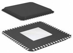
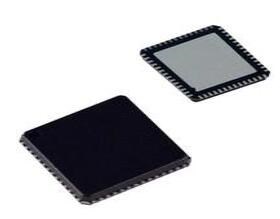
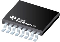
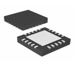
CD4011 Package

CD4011 Manufacturer
Texas Instruments (TI) is an American technology company headquartered in Dallas, Texas, which designs and manufactures semiconductors and various integrated circuits, and sells them to electronic designers and manufacturers worldwide. It is one of the top 10 semiconductor companies in global sales. The company focuses on the development of analog chips and embedded processors, which account for more than 80% of its revenue. TI also produces TI digital light processing technology and educational technology products, including calculators, microcontrollers and multi-core processors. As of 2016, the company has 45,000 patents worldwide.
Trend Analysis
Datasheet PDF
- PCN Design/Specification :
- Datasheets :
CD4011BE-Texas-Instruments-datasheet-102486840.pdf
CD4011BE-Texas-Instruments-datasheet-31668920.pdf
CD4011BE-Texas-Instruments-datasheet-47642636.pdf
CD4011BE-Texas-Instruments-datasheet-14147894.pdf
CD4011BE-Texas-Instruments-datasheet-10253768.pdf
CD4011BE-Texas-Instruments-datasheet-7277804.pdf
CD4011BE-Texas-Instruments-datasheet-10447.pdf
1.What is CD4011?
The integrated circuit CD4011 is a CMOS circuit containing 4 NAND gates, each NAND gate has 2 input terminals and one output terminal. When one of the two input terminals is 0, the output is 0. Only when the inputs are all 1, the output is 1. When both input terminals are 0, the output is 1
2.What is the difference between CD4011 and 74HC00P?
CD4011 and 74HC00P are two-input four-NAND gates. The pin layout of the two chips is different. Both chips are CMOS devices.
The operating voltage range of CD4011 power supply is 3V ~ 18V. The operating voltage range of 74HC00P is 2V ~ 6V.
Both CD4011 and 74HC00 are 2-input four-NAND gates. The pin arrangement of CD4011 and 74CC00 is different. CD4011 is a CMOS device with a power supply voltage of 3V-18V. 74HC00 is a high-speed CMOS device with a power supply voltage of 2V-6V.
3.What is the difference between CD4093 and CD4011?
Both CD4093 and CD4011 are four 2-input NAND gates with the same pin arrangement. CD4011 is a common NAND gate and CD4093 is a NAND gate with Schmitt trigger function.
 2SC5200 vs.TTC5200
08 July 202213510
 TDA2050 Amplifier: Datasheet, Circuit, Replacement
29 October 202124262
 W25Q16JVSNIQ: Overview, Features, and Applications
28 November 20231623
 M10385 FM Module:Datasheet, Application, Schematic
01 September 2021803
 SI5347 Clock Generator: Features, Pinout and Datasheet
18 April 20221006
 AD9959 Frequency Synthesizer: Pinout, Datasheet, Application Circuit
28 September 20211629
 MAX3232 Line Receiver: Features, Speicifications and Applications
21 May 20211412
 MCP2515 CAN Controller: Datasheet, Pinout, Block Diagram
15 September 202111699
 Silicon Carbide Semiconductor Devices at Ultra-high Voltages and their Applications
04 January 20231946
 The Reason for the Leakage Current of MOS Tube
26 March 20228035
 What is Relay?
15 November 20217130
 Amorphous Silicon Solar Cells: Features, Structure and Applications
22 August 20225764
 Design and Implementation of High Frequency Inverter for Printer Based on IR2110
13 April 20229342
 C1815 vs C945 Key Features and Application Guide
01 September 20253026
 Introduction to DC Amplifier
07 November 202517591
 What is a USB Type-C Connector?
28 October 20255743
Texas Instruments
In Stock: 1005
United States
China
Canada
Japan
Russia
Germany
United Kingdom
Singapore
Italy
Hong Kong(China)
Taiwan(China)
France
Korea
Mexico
Netherlands
Malaysia
Austria
Spain
Switzerland
Poland
Thailand
Vietnam
India
United Arab Emirates
Afghanistan
Åland Islands
Albania
Algeria
American Samoa
Andorra
Angola
Anguilla
Antigua & Barbuda
Argentina
Armenia
Aruba
Australia
Azerbaijan
Bahamas
Bahrain
Bangladesh
Barbados
Belarus
Belgium
Belize
Benin
Bermuda
Bhutan
Bolivia
Bonaire, Sint Eustatius and Saba
Bosnia & Herzegovina
Botswana
Brazil
British Indian Ocean Territory
British Virgin Islands
Brunei
Bulgaria
Burkina Faso
Burundi
Cabo Verde
Cambodia
Cameroon
Cayman Islands
Central African Republic
Chad
Chile
Christmas Island
Cocos (Keeling) Islands
Colombia
Comoros
Congo
Congo (DRC)
Cook Islands
Costa Rica
Côte d’Ivoire
Croatia
Cuba
Curaçao
Cyprus
Czechia
Denmark
Djibouti
Dominica
Dominican Republic
Ecuador
Egypt
El Salvador
Equatorial Guinea
Eritrea
Estonia
Eswatini
Ethiopia
Falkland Islands
Faroe Islands
Fiji
Finland
French Guiana
French Polynesia
Gabon
Gambia
Georgia
Ghana
Gibraltar
Greece
Greenland
Grenada
Guadeloupe
Guam
Guatemala
Guernsey
Guinea
Guinea-Bissau
Guyana
Haiti
Honduras
Hungary
Iceland
Indonesia
Iran
Iraq
Ireland
Isle of Man
Israel
Jamaica
Jersey
Jordan
Kazakhstan
Kenya
Kiribati
Kosovo
Kuwait
Kyrgyzstan
Laos
Latvia
Lebanon
Lesotho
Liberia
Libya
Liechtenstein
Lithuania
Luxembourg
Macao(China)
Madagascar
Malawi
Maldives
Mali
Malta
Marshall Islands
Martinique
Mauritania
Mauritius
Mayotte
Micronesia
Moldova
Monaco
Mongolia
Montenegro
Montserrat
Morocco
Mozambique
Myanmar
Namibia
Nauru
Nepal
New Caledonia
New Zealand
Nicaragua
Niger
Nigeria
Niue
Norfolk Island
North Korea
North Macedonia
Northern Mariana Islands
Norway
Oman
Pakistan
Palau
Palestinian Authority
Panama
Papua New Guinea
Paraguay
Peru
Philippines
Pitcairn Islands
Portugal
Puerto Rico
Qatar
Réunion
Romania
Rwanda
Samoa
San Marino
São Tomé & Príncipe
Saudi Arabia
Senegal
Serbia
Seychelles
Sierra Leone
Sint Maarten
Slovakia
Slovenia
Solomon Islands
Somalia
South Africa
South Sudan
Sri Lanka
St Helena, Ascension, Tristan da Cunha
St. Barthélemy
St. Kitts & Nevis
St. Lucia
St. Martin
St. Pierre & Miquelon
St. Vincent & Grenadines
Sudan
Suriname
Svalbard & Jan Mayen
Sweden
Syria
Tajikistan
Tanzania
Timor-Leste
Togo
Tokelau
Tonga
Trinidad & Tobago
Tunisia
Turkey
Turkmenistan
Turks & Caicos Islands
Tuvalu
U.S. Outlying Islands
U.S. Virgin Islands
Uganda
Ukraine
Uruguay
Uzbekistan
Vanuatu
Vatican City
Venezuela
Wallis & Futuna
Yemen
Zambia
Zimbabwe
![SN7402N]() SN7402N
SN7402NTexas Instruments
![SN7405N]() SN7405N
SN7405NTexas Instruments
![SN74AS1000AN]() SN74AS1000AN
SN74AS1000ANTexas Instruments
![SN74ALS1005N]() SN74ALS1005N
SN74ALS1005NTexas Instruments
![SN74ALS20ANSR]() SN74ALS20ANSR
SN74ALS20ANSRTexas Instruments
![SN74ALS1004N]() SN74ALS1004N
SN74ALS1004NTexas Instruments
![SN74ALS11ANS]() SN74ALS11ANS
SN74ALS11ANSTexas Instruments
![SN7404N]() SN7404N
SN7404NTexas Instruments
![SN74ALS1005NSR]() SN74ALS1005NSR
SN74ALS1005NSRTexas Instruments
![SN74F38DR]() SN74F38DR
SN74F38DRTexas Instruments


