
 Product
 Brand
Brand Articles
 Tools
Tools
CD4027 JK Flip-Flop IC:Pinout, Diagram and Datasheet

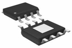
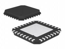
3V~18V 24MHz JK Type Flip Flop DUAL CD4027 16 Pins 4μA 4000B Series 16-SOIC (0.154, 3.90mm Width)


3V~18V 24MHz JK Type Flip Flop DUAL CD4027 16 Pins 4μA 4000B Series 16-SOIC (0.154, 3.90mm Width)
CD4027 is a dual package JK flip-flop IC. This article mainly introduce pinout,diagram, datasheet and other detailed information about Texas Instruments CD4027.

CD4027 based 4 bit up counter simulation in Proteus
CD4027 Description
CD4027 is a CMOS based high voltage high speed Dual JK Flip-Flop that is generally used for data storing. The Flip-Flop could typically operate at a speed of 16MHz even at high voltages like 15V with a low noise margin of only 2.5V.
Two similar or equal JK flip flops are contained in the IC. Each pair of JK flip flop with IC has provision of pins J, K, set, reset along with clock and with two output terminals which are complimentary of each other.
JK flip flop can be employed in the applications like voice register, counters or else as a control circuit.
CD4027 Pinout


CD4027 CAD Model
Symbol

Footprint

3D Model

CD4027 Features
●Dual JK Flip Flop Package IC
●Operating Speed: 16MHz( medium speed)
●Operating Voltage: 5V, 10V, 15V
●Maximum Operating Voltage: 20V
●Input Rise/Fall time at 5V : 45us
●Minimum High Level Input Voltage: 2 V
●Maximum Low Level Input Voltage: 0.8 V
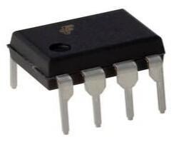
●Available in 14-pin PDIP, GDIP, PDSO packages
●Static Flip-Flop Operation retains state indefinitely
●High noise immunity of 0.45 VDD(typ.)
●Set and Reset capability
●TTL compatible
●Low power of 50 nW (typ.)
●Set-reset capability
●With clock level either high or low
●Toggle rate at 10 V
●Standardized symmetrical output characteristics
●100% tested for quiescent current at 20 V
●Maximum input current of 1 μA at 18 V over full package-temperature range; 100 nA at 18 V and 25°C
●Noise margin (over full package-temperature range):
– 1 V at VDD = 5 V
– 2 V at VDD = 10 V
– 2.5 V at VDD = 15 V
Specifications
- TypeParameter
- Lifecycle Status
Lifecycle Status refers to the current stage of an electronic component in its product life cycle, indicating whether it is active, obsolete, or transitioning between these states. An active status means the component is in production and available for purchase. An obsolete status indicates that the component is no longer being manufactured or supported, and manufacturers typically provide a limited time frame for support. Understanding the lifecycle status is crucial for design engineers to ensure continuity and reliability in their projects.
ACTIVE (Last Updated: 3 days ago) - Factory Lead Time6 Weeks
- Contact Plating
Contact plating (finish) provides corrosion protection for base metals and optimizes the mechanical and electrical properties of the contact interfaces.
Gold - Mount
In electronic components, the term "Mount" typically refers to the method or process of physically attaching or fixing a component onto a circuit board or other electronic device. This can involve soldering, adhesive bonding, or other techniques to secure the component in place. The mounting process is crucial for ensuring proper electrical connections and mechanical stability within the electronic system. Different components may have specific mounting requirements based on their size, shape, and function, and manufacturers provide guidelines for proper mounting procedures to ensure optimal performance and reliability of the electronic device.
Surface Mount - Mounting Type
The "Mounting Type" in electronic components refers to the method used to attach or connect a component to a circuit board or other substrate, such as through-hole, surface-mount, or panel mount.
Surface Mount - Package / Case
refers to the protective housing that encases an electronic component, providing mechanical support, electrical connections, and thermal management.
16-SOIC (0.154, 3.90mm Width) - Number of Pins16
- Weight141.690917mg
- Clock-Edge Trigger TypePositive Edge
- Operating Temperature
The operating temperature is the range of ambient temperature within which a power supply, or any other electrical equipment, operate in. This ranges from a minimum operating temperature, to a peak or maximum operating temperature, outside which, the power supply may fail.
-55°C~125°C TA - Packaging
Semiconductor package is a carrier / shell used to contain and cover one or more semiconductor components or integrated circuits. The material of the shell can be metal, plastic, glass or ceramic.
Tube - Series
In electronic components, the "Series" refers to a group of products that share similar characteristics, designs, or functionalities, often produced by the same manufacturer. These components within a series typically have common specifications but may vary in terms of voltage, power, or packaging to meet different application needs. The series name helps identify and differentiate between various product lines within a manufacturer's catalog.
4000B - JESD-609 Code
The "JESD-609 Code" in electronic components refers to a standardized marking code that indicates the lead-free solder composition and finish of electronic components for compliance with environmental regulations.
e4 - Pbfree Code
The "Pbfree Code" parameter in electronic components refers to the code or marking used to indicate that the component is lead-free. Lead (Pb) is a toxic substance that has been widely used in electronic components for many years, but due to environmental concerns, there has been a shift towards lead-free alternatives. The Pbfree Code helps manufacturers and users easily identify components that do not contain lead, ensuring compliance with regulations and promoting environmentally friendly practices. It is important to pay attention to the Pbfree Code when selecting electronic components to ensure they meet the necessary requirements for lead-free applications.
yes - Part Status
Parts can have many statuses as they progress through the configuration, analysis, review, and approval stages.
Active - Moisture Sensitivity Level (MSL)
Moisture Sensitivity Level (MSL) is a standardized rating that indicates the susceptibility of electronic components, particularly semiconductors, to moisture-induced damage during storage and the soldering process, defining the allowable exposure time to ambient conditions before they require special handling or baking to prevent failures
1 (Unlimited) - Number of Terminations16
- ECCN Code
An ECCN (Export Control Classification Number) is an alphanumeric code used by the U.S. Bureau of Industry and Security to identify and categorize electronic components and other dual-use items that may require an export license based on their technical characteristics and potential for military use.
EAR99 - TypeJK Type
- Voltage - Supply
Voltage - Supply refers to the range of voltage levels that an electronic component or circuit is designed to operate with. It indicates the minimum and maximum supply voltage that can be applied for the device to function properly. Providing supply voltages outside this range can lead to malfunction, damage, or reduced performance. This parameter is critical for ensuring compatibility between different components in a circuit.
3V~18V - Terminal Position
In electronic components, the term "Terminal Position" refers to the physical location of the connection points on the component where external electrical connections can be made. These connection points, known as terminals, are typically used to attach wires, leads, or other components to the main body of the electronic component. The terminal position is important for ensuring proper connectivity and functionality of the component within a circuit. It is often specified in technical datasheets or component specifications to help designers and engineers understand how to properly integrate the component into their circuit designs.
DUAL - Terminal Form
Occurring at or forming the end of a series, succession, or the like; closing; concluding.
GULL WING - Peak Reflow Temperature (Cel)
Peak Reflow Temperature (Cel) is a parameter that specifies the maximum temperature at which an electronic component can be exposed during the reflow soldering process. Reflow soldering is a common method used to attach electronic components to a circuit board. The Peak Reflow Temperature is crucial because it ensures that the component is not damaged or degraded during the soldering process. Exceeding the specified Peak Reflow Temperature can lead to issues such as component failure, reduced performance, or even permanent damage to the component. It is important for manufacturers and assemblers to adhere to the recommended Peak Reflow Temperature to ensure the reliability and functionality of the electronic components.
260 - Supply Voltage
Supply voltage refers to the electrical potential difference provided to an electronic component or circuit. It is crucial for the proper operation of devices, as it powers their functions and determines performance characteristics. The supply voltage must be within specified limits to ensure reliability and prevent damage to components. Different electronic devices have specific supply voltage requirements, which can vary widely depending on their design and intended application.
5V - Base Part Number
The "Base Part Number" (BPN) in electronic components serves a similar purpose to the "Base Product Number." It refers to the primary identifier for a component that captures the essential characteristics shared by a group of similar components. The BPN provides a fundamental way to reference a family or series of components without specifying all the variations and specific details.
CD4027 - Function
The parameter "Function" in electronic components refers to the specific role or purpose that the component serves within an electronic circuit. It defines how the component interacts with other elements, influences the flow of electrical signals, and contributes to the overall behavior of the system. Functions can include amplification, signal processing, switching, filtering, and energy storage, among others. Understanding the function of each component is essential for designing effective and efficient electronic systems.
Set(Preset) and Reset - Output Type
The "Output Type" parameter in electronic components refers to the type of signal or data that is produced by the component as an output. This parameter specifies the nature of the output signal, such as analog or digital, and can also include details about the voltage levels, current levels, frequency, and other characteristics of the output signal. Understanding the output type of a component is crucial for ensuring compatibility with other components in a circuit or system, as well as for determining how the output signal can be utilized or processed further. In summary, the output type parameter provides essential information about the nature of the signal that is generated by the electronic component as its output.
Differential - Polarity
In electronic components, polarity refers to the orientation or direction in which the component must be connected in a circuit to function properly. Components such as diodes, capacitors, and LEDs have polarity markings to indicate which terminal should be connected to the positive or negative side of the circuit. Connecting a component with incorrect polarity can lead to malfunction or damage. It is important to pay attention to polarity markings and follow the manufacturer's instructions to ensure proper operation of electronic components.
Non-Inverting - Supply Voltage-Min (Vsup)
The parameter "Supply Voltage-Min (Vsup)" in electronic components refers to the minimum voltage level required for the component to operate within its specified performance range. This parameter indicates the lowest voltage that can be safely applied to the component without risking damage or malfunction. It is crucial to ensure that the supply voltage provided to the component meets or exceeds this minimum value to ensure proper functionality and reliability. Failure to adhere to the specified minimum supply voltage may result in erratic behavior, reduced performance, or even permanent damage to the component.
3V - Number of Channels2
- Load Capacitance
the amount of capacitance measured or computed across the crystal terminals on the PCB. Frequency Tolerance. Frequency tolerance refers to the allowable deviation from nominal, in parts per million (PPM), at a specific temperature, usually +25°C.
50pF - Output Current
The rated output current is the maximum load current that a power supply can provide at a specified ambient temperature. A power supply can never provide more current that it's rated output current unless there is a fault, such as short circuit at the load.
6.8mA - Clock Frequency
Clock frequency, also known as clock speed, refers to the rate at which a processor or electronic component can execute instructions. It is measured in hertz (Hz) and represents the number of cycles per second that the component can perform. A higher clock frequency typically indicates a faster processing speed and better performance. However, it is important to note that other factors such as architecture, efficiency, and workload also play a significant role in determining the overall performance of a component. In summary, clock frequency is a crucial parameter that influences the speed and efficiency of electronic components in processing data and executing tasks.
24MHz - Propagation Delay
the flight time of packets over the transmission link and is limited by the speed of light.
300 ns - Quiescent Current
The quiescent current is defined as the current level in the amplifier when it is producing an output of zero.
20μA - Turn On Delay Time
Turn-on delay, td(on), is the time taken to charge the input capacitance of the device before drain current conduction can start.
45 ns - Logic Function
In electronic components, the term "Logic Function" refers to the specific operation or behavior of a component based on its input signals. It describes how the component processes the input signals to produce the desired output. Logic functions are fundamental to digital circuits and are used to perform logical operations such as AND, OR, NOT, and XOR.Each electronic component, such as logic gates or flip-flops, is designed to perform a specific logic function based on its internal circuitry. By understanding the logic function of a component, engineers can design and analyze complex digital systems to ensure proper functionality and performance. Different logic functions can be combined to create more complex operations, allowing for the creation of sophisticated digital devices and systems.
AND, Flip-Flop, JK-Type - Current - Quiescent (Iq)
The parameter "Current - Quiescent (Iq)" in electronic components refers to the amount of current consumed by a device when it is in a quiescent or idle state, meaning when it is not actively performing any tasks or operations. This parameter is important because it represents the baseline power consumption of the device even when it is not actively being used. A lower quiescent current (Iq) value is desirable as it indicates that the device is more energy-efficient and will consume less power when not in use, which can help extend battery life in portable devices and reduce overall power consumption in electronic systems. Designers often pay close attention to the quiescent current specification when selecting components for low-power applications or battery-operated devices.
4μA - Number of Bits per Element1
- Max Propagation Delay @ V, Max CL
The parameter "Max Propagation Delay @ V, Max CL" in electronic components refers to the maximum amount of time it takes for a signal to propagate through the component from input to output when operating at a specific voltage (V) and driving a maximum specified load capacitance (CL). This parameter is crucial in determining the speed and performance of the component in a circuit. A shorter propagation delay indicates faster signal processing and better overall performance. Designers use this parameter to ensure that signals can be transmitted and received within the required timing constraints in their electronic systems.
90ns @ 15V, 50pF - Trigger Type
Trigger Type in electronic components refers to the mechanism or method by which a device, such as a flip-flop or timer, responds to an input signal. It defines how the device transitions between states based on specific conditions, such as rising or falling edges of a signal, levels, or pulses. Different trigger types such as edge-triggered, level-triggered, or pulse-triggered influence the timing and behavior of the circuit, thereby determining how input signals affect the output in various applications.
Positive Edge - Input Capacitance
The capacitance between the input terminals of an op amp with either input grounded. It is expressed in units of farads.
5pF - Power Supply Current-Max (ICC)
The parameter "Power Supply Current-Max (ICC)" in electronic components refers to the maximum amount of current that the component will draw from the power supply under specified operating conditions. It is an important specification as it helps determine the power consumption of the component and ensures that the power supply can provide enough current to meet the component's requirements without being overloaded. Exceeding the maximum power supply current can lead to overheating, component damage, or system failure. Designers use this parameter to select an appropriate power supply and ensure the reliable operation of the electronic system.
0.06mA - Max Frequency@Nom-Sup
The parameter "Max Frequency@Nom-Sup" in electronic components refers to the maximum operating frequency at nominal supply voltage. This parameter indicates the highest frequency at which the component can function reliably when supplied with its specified voltage. It is an important specification for components such as microcontrollers, processors, and other digital devices that operate based on clock signals. Exceeding the maximum frequency can lead to errors, malfunctions, or even damage to the component. Designers and engineers use this parameter to ensure that the component operates within its specified limits for optimal performance and reliability.
3500000Hz - Height1.75mm
- Length9.9mm
- Width3.91mm
- Thickness
Thickness in electronic components refers to the measurement of how thick a particular material or layer is within the component structure. It can pertain to various aspects, such as the thickness of a substrate, a dielectric layer, or conductive traces. This parameter is crucial as it impacts the electrical, mechanical, and thermal properties of the component, influencing its performance and reliability in electronic circuits.
1.58mm - REACH SVHC
The parameter "REACH SVHC" in electronic components refers to the compliance with the Registration, Evaluation, Authorization, and Restriction of Chemicals (REACH) regulation regarding Substances of Very High Concern (SVHC). SVHCs are substances that may have serious effects on human health or the environment, and their use is regulated under REACH to ensure their safe handling and minimize their impact.Manufacturers of electronic components need to declare if their products contain any SVHCs above a certain threshold concentration and provide information on the safe use of these substances. This information allows customers to make informed decisions about the potential risks associated with using the components and take appropriate measures to mitigate any hazards.Ensuring compliance with REACH SVHC requirements is essential for electronics manufacturers to meet regulatory standards, protect human health and the environment, and maintain transparency in their supply chain. It also demonstrates a commitment to sustainability and responsible manufacturing practices in the electronics industry.
No SVHC - Radiation Hardening
Radiation hardening is the process of making electronic components and circuits resistant to damage or malfunction caused by high levels of ionizing radiation, especially for environments in outer space (especially beyond the low Earth orbit), around nuclear reactors and particle accelerators, or during nuclear accidents or nuclear warfare.
No - RoHS Status
RoHS means “Restriction of Certain Hazardous Substances” in the “Hazardous Substances Directive” in electrical and electronic equipment.
ROHS3 Compliant - Lead Free
Lead Free is a term used to describe electronic components that do not contain lead as part of their composition. Lead is a toxic material that can have harmful effects on human health and the environment, so the electronics industry has been moving towards lead-free components to reduce these risks. Lead-free components are typically made using alternative materials such as silver, copper, and tin. Manufacturers must comply with regulations such as the Restriction of Hazardous Substances (RoHS) directive to ensure that their products are lead-free and environmentally friendly.
Lead Free
CD4027 Functional Block Diagram

CD4027 Alternatives

Where to use CD4027?
The CD4027 is a dual in-line JK flip flop IC. Meaning it has two JK flip flops inside it and each can be used individually based on our application. The term JK flip flop comes after its inventor Jack Kilby.
The JK flip flops are considered to be the most efficient flip-flop and can be used for certain applications on its own. The flip-flops are also called as latching devices meaning it can remember one single bit of data and latch the output based on it, due to this property they are commonly used as shift registers, control registers, storage registers or where ever a small memory is required.
More than one Flip Flop can be used in series to act as an EEPROM for holding small amount of data. The JK flip flop is considered to be more suitable for practical application because of its truth table that is the output of the flip flop will be stable for all types of inputs.
So if you are looking for a IC for latching purpose or to act as a small programmable memory for you project then this IC might be the right choice for you.
How to use CD4027?
As told earlier we have two JK flip flops in this IC, the IC is powered by +5V typically the minimum and maximum input and output voltage for the input (J,K) pins and the output (Q, Q bar) pins are discussed in the specifications above. The below circuit shows a typical sample connection for the JK flip-flop.

The J and K pins are the input pins for the Flip-Flop and the Q and Q bar pins are the output pins. Note that the input pins are pulled down to ground through a 1k resistor or less, this way we can avoid the pin in floating condition. That is the pin will held to ground when the button is not pressed and when the button is pressed the pin will be held to supply voltage.
The reset button should be pulled up through a 1K resistor and when grounded will reset the flip-flop. The clock signal for the JK flip-flop is responsible for changing the state of the output. The flip-flop will change its output only during the rising edge of the clock signal. The clock signal here is just a push button but can be type of pulse like a PWM signal. The output state of the flip flops can be determined form the truth table below.

Normally during regular operation of the IC the reset pin will be set high and the clock pulse of known frequency will be supplied to the clock pin, then the value o J and K will be varied based on the input signals and the respective output will be obtained on the Q and Q bar pins. This region of operation in highlighted in red colour on the Truth table above.
CD4027 Applications
●Shift Registers
●Voice registers and Memory or Control Registers
●EEPROM circuits
●Latching devices
●Registers, control circuits,Latching devices and Counters
●Computer memory circuits
CD4027 Package

CD4027 Manufacturer
Texas Instruments (TI) is an American technology company headquartered in Dallas, Texas, which designs and manufactures semiconductors and various integrated circuits, and sells them to electronic designers and manufacturers worldwide. It is one of the top 10 semiconductor companies in global sales. The company focuses on the development of analog chips and embedded processors, which account for more than 80% of its revenue. TI also produces TI digital light processing technology and educational technology products, including calculators, microcontrollers and multi-core processors. As of 2016, the company has 45,000 patents worldwide.
Trend Analysis
Datasheet PDF
- PCN Design/Specification :
- Datasheets :
1.What is the difference between CD4027 and 74LS112? Which circuit is better for the two?
(1). CD4027 is a CMOS device with a wide operating power supply voltage range (3V~18V), while 74LS112 is a TTL device, which can only work within the voltage range of 5V±0.5V;
(2). CD4027 is a rising edge trigger, and 74LS112 is a falling edge trigger;
(3). The delay time of 74LS is much smaller than that of CD4027;
(4). CD4027 has higher input impedance, larger fan-out coefficient and lower power consumption, while 74LS112 has stronger drive capability;
(5). The order of their pins is also different.
According to the above-mentioned respective characteristics, select the application occasions. For example, if the working voltage is only about 3V or higher than 6V, choose CD4027; when working at about 5V and hope to have a stronger driving ability, choose 74LS112.
2.Is there any difference between CD4027 in-line and patch? What's the difference?
The chip packaging form is different, the pin position and function are the same.
3.What circuit is composed of electronic circuit CD4027?
CD4027 contains two independent, complementary and symmetrical J-K master-slave flip-flop monolithic integrated circuits.
Each flip-flop provides J, K, set, reset, clock input, and buffered Q and Q non-output signals. This device can be used as a shift register, and by connecting the Q output to the data input, it can be used as a counter and flip-flop. When the rising edge of the clock triggers, the logic level added to the D input terminal is transferred to the Q output terminal. Set and reset have nothing to do with the clock, but are completed by the high level on the set or reset line respectively.
 XRP7675 Step-Down Regulator: Pinout, Features and Datasheet
16 March 2022786
 MCP4151 Dual SPI Digital POT: Pinout, Equivalent and Datasheet
31 December 20213707
 FOD3180 Optocoupler: Application, Circuit, Datasheet
20 October 20212579
 xc6220b331mr-g:LDO Voltage Regulators 1A High Speed Green Operation Vltg Reg
03 March 20221238
 ATMEGA328P-MU AVR 8-bit Microcontrollers - MCU 32KB In-system: Datasheet, Pinout, and Equivalents
24 February 20223565
 Top-Rated Suppliers of ADIS16209CCCZ Sensors
07 June 2025129
 An In-Depth Look at the LTC6602IUF#TRPBF Active Filter: Features, Applications, and Reference Designs
06 March 2024149
 2N2905A PNP Transistor: Pinout, Datasheet, and Equivalents
29 July 20215905
 Development Board History and Differences from Single Board Computers (SBCs)
16 May 20225618
 What is Keyboard and How to Choose It?
17 February 20226446
 Silicon Carbide (SiC): The Third-generation Semiconductor Material
30 August 20219334
 Huawei's Sensor Layout
24 March 20222465
 Enhancing Frequency Stability in Modern Distributed Power Systems
21 September 20243947
 What is PWM "Dead Band"?
21 April 20226867
 How to Choose the Right Spade Connector for Any Project
18 July 20256588
 Why Precision Matters in Analog-to-Digital Conversion
28 May 2025820
Texas Instruments
In Stock: 309
United States
China
Canada
Japan
Russia
Germany
United Kingdom
Singapore
Italy
Hong Kong(China)
Taiwan(China)
France
Korea
Mexico
Netherlands
Malaysia
Austria
Spain
Switzerland
Poland
Thailand
Vietnam
India
United Arab Emirates
Afghanistan
Åland Islands
Albania
Algeria
American Samoa
Andorra
Angola
Anguilla
Antigua & Barbuda
Argentina
Armenia
Aruba
Australia
Azerbaijan
Bahamas
Bahrain
Bangladesh
Barbados
Belarus
Belgium
Belize
Benin
Bermuda
Bhutan
Bolivia
Bonaire, Sint Eustatius and Saba
Bosnia & Herzegovina
Botswana
Brazil
British Indian Ocean Territory
British Virgin Islands
Brunei
Bulgaria
Burkina Faso
Burundi
Cabo Verde
Cambodia
Cameroon
Cayman Islands
Central African Republic
Chad
Chile
Christmas Island
Cocos (Keeling) Islands
Colombia
Comoros
Congo
Congo (DRC)
Cook Islands
Costa Rica
Côte d’Ivoire
Croatia
Cuba
Curaçao
Cyprus
Czechia
Denmark
Djibouti
Dominica
Dominican Republic
Ecuador
Egypt
El Salvador
Equatorial Guinea
Eritrea
Estonia
Eswatini
Ethiopia
Falkland Islands
Faroe Islands
Fiji
Finland
French Guiana
French Polynesia
Gabon
Gambia
Georgia
Ghana
Gibraltar
Greece
Greenland
Grenada
Guadeloupe
Guam
Guatemala
Guernsey
Guinea
Guinea-Bissau
Guyana
Haiti
Honduras
Hungary
Iceland
Indonesia
Iran
Iraq
Ireland
Isle of Man
Israel
Jamaica
Jersey
Jordan
Kazakhstan
Kenya
Kiribati
Kosovo
Kuwait
Kyrgyzstan
Laos
Latvia
Lebanon
Lesotho
Liberia
Libya
Liechtenstein
Lithuania
Luxembourg
Macao(China)
Madagascar
Malawi
Maldives
Mali
Malta
Marshall Islands
Martinique
Mauritania
Mauritius
Mayotte
Micronesia
Moldova
Monaco
Mongolia
Montenegro
Montserrat
Morocco
Mozambique
Myanmar
Namibia
Nauru
Nepal
New Caledonia
New Zealand
Nicaragua
Niger
Nigeria
Niue
Norfolk Island
North Korea
North Macedonia
Northern Mariana Islands
Norway
Oman
Pakistan
Palau
Palestinian Authority
Panama
Papua New Guinea
Paraguay
Peru
Philippines
Pitcairn Islands
Portugal
Puerto Rico
Qatar
Réunion
Romania
Rwanda
Samoa
San Marino
São Tomé & Príncipe
Saudi Arabia
Senegal
Serbia
Seychelles
Sierra Leone
Sint Maarten
Slovakia
Slovenia
Solomon Islands
Somalia
South Africa
South Sudan
Sri Lanka
St Helena, Ascension, Tristan da Cunha
St. Barthélemy
St. Kitts & Nevis
St. Lucia
St. Martin
St. Pierre & Miquelon
St. Vincent & Grenadines
Sudan
Suriname
Svalbard & Jan Mayen
Sweden
Syria
Tajikistan
Tanzania
Timor-Leste
Togo
Tokelau
Tonga
Trinidad & Tobago
Tunisia
Turkey
Turkmenistan
Turks & Caicos Islands
Tuvalu
U.S. Outlying Islands
U.S. Virgin Islands
Uganda
Ukraine
Uruguay
Uzbekistan
Vanuatu
Vatican City
Venezuela
Wallis & Futuna
Yemen
Zambia
Zimbabwe
![SN74LVC1G175DCKR]() SN74LVC1G175DCKR
SN74LVC1G175DCKRTexas Instruments
![SN74AHC74RGYR]() SN74AHC74RGYR
SN74AHC74RGYRTexas Instruments
![SN74LVC2G74DCTR]() SN74LVC2G74DCTR
SN74LVC2G74DCTRTexas Instruments
![SN74LVC2G74DCUR]() SN74LVC2G74DCUR
SN74LVC2G74DCURTexas Instruments
![SN74HC74PWR]() SN74HC74PWR
SN74HC74PWRTexas Instruments
![SN74HC74DR]() SN74HC74DR
SN74HC74DRTexas Instruments
![SN74HC273DWR]() SN74HC273DWR
SN74HC273DWRTexas Instruments
![SN74HC273DW]() SN74HC273DW
SN74HC273DWTexas Instruments
![SN74HC175DR]() SN74HC175DR
SN74HC175DRTexas Instruments
![CD4013BM]() CD4013BM
CD4013BMTexas Instruments


