
 Product
 Brand
Brand Articles
 Tools
Tools
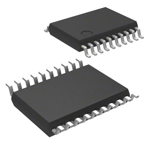
CD4051BM Analog Switch: Pinout, CAD Model and Specification

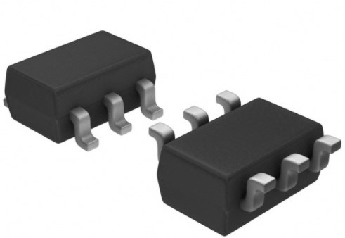
240Ohm Analog Switches BREAK-BEFORE-MAKE CD4051 16 Pins 100nA 5V 16-SOIC (0.154, 3.90mm Width)


240Ohm Analog Switches BREAK-BEFORE-MAKE CD4051 16 Pins 100nA 5V 16-SOIC (0.154, 3.90mm Width)
The CD4051BM analog multiplexers and demuliplexers are digitally-controlled analog switches having low ON impedance and very low OFF leakage current. This blog mainly introduces pinout, equivalents, applications, and other detailed information about Texas Instruments CD4051BM.
CD4051 Analog Switch / Multiplexer / Demultiplexer
CD4051BM Description
The CD4051B analog multiplexers are digitally-controlled analog switches having low ON impedance and very low OFF leakage current. Control of analog signals up to 20 VP-P can be achieved by digital signal amplitudes of 4.5 V to 20 V (if VDD – VSS = 3 V, a VDD – VEE of up to 13 V can be controlled; for VDD – VEE level differences above 13 V, a VDD – VSS of at least 4.5 V is required). For example, if VDD = +4.5 V, VSS = 0 V, and VEE = –13.5 V, analog signals from –13.5 V to +4.5 V can be controlled by digital inputs of 0 V to 5 V. These multiplexer circuits dissipate extremely low quiescent power over the full VDD – VSS and VDD – VEE supply-voltage ranges, independent of the logic state of the control signals. When logic 1 is present at the inhibit input terminal, all channels are off.
The CD4051B device is a single 8-channel multiplexer having three binary control inputs, A, B, and C, and an inhibit input. The three binary signals select 1 of 8 channels to be turned on and connect one of the 8 inputs to the output.
CD4051BM Pinout


Pin Functions CD4051B
CD4051BM CAD Model

PCB Symbol - Texas Instruments CD4051BM

PCB Footprint - Texas Instruments CD4051BM

3D Model - Texas Instruments CD4051BM
CD4051BM Features
• Wide Range of Digital and Analog Signal Levels
– Digital: 3 V to 20 V
– Analog: ≤20 VP-P
• Low ON Resistance,125 Ω (Typical) Over 15 VP-P Signal Input Range for VDD – VEE = 18 V
• High OFF Resistance, Channel Leakage of ±100 pA (Typical) at VDD – VEE = 18 V
• Logic-Level Conversion for Digital Addressing
Signals of 3 V to 20 V (VDD – VSS = 3 V to 20 V) to Switch Analog Signals to 20 VP-P (VDD – VEE = 20 V) Matched Switch Characteristics, rON = 5 Ω (Typical) for VDD – VEE = 15 V Very Low Quiescent Power Dissipation Under All Digital-Control Input and Supply Conditions, 0.2 µW (Typical) at VDD – VSS = VDD – VEE = 10 V
• Binary Address Decoding on Chip
• 5 V, 10 V, and 15 V Parametric Ratings
• 100% Tested for Quiescent Current at 20 V
• Maximum Input Current of 1 µA at 18 V Over Full Package Temperature Range, 100 nA at 18 V and 25°C
• Break-Before-Make Switching Eliminates Channel Overlap
Specifications
- TypeParameter
- Lifecycle Status
Lifecycle Status refers to the current stage of an electronic component in its product life cycle, indicating whether it is active, obsolete, or transitioning between these states. An active status means the component is in production and available for purchase. An obsolete status indicates that the component is no longer being manufactured or supported, and manufacturers typically provide a limited time frame for support. Understanding the lifecycle status is crucial for design engineers to ensure continuity and reliability in their projects.
ACTIVE (Last Updated: 3 days ago) - Factory Lead Time6 Weeks
- Contact Plating
Contact plating (finish) provides corrosion protection for base metals and optimizes the mechanical and electrical properties of the contact interfaces.
Gold - Mount
In electronic components, the term "Mount" typically refers to the method or process of physically attaching or fixing a component onto a circuit board or other electronic device. This can involve soldering, adhesive bonding, or other techniques to secure the component in place. The mounting process is crucial for ensuring proper electrical connections and mechanical stability within the electronic system. Different components may have specific mounting requirements based on their size, shape, and function, and manufacturers provide guidelines for proper mounting procedures to ensure optimal performance and reliability of the electronic device.
Surface Mount - Mounting Type
The "Mounting Type" in electronic components refers to the method used to attach or connect a component to a circuit board or other substrate, such as through-hole, surface-mount, or panel mount.
Surface Mount - Package / Case
refers to the protective housing that encases an electronic component, providing mechanical support, electrical connections, and thermal management.
16-SOIC (0.154, 3.90mm Width) - Number of Pins16
- Weight141.690917mg
- Turn Off Delay Time
It is the time from when Vgs drops below 90% of the gate drive voltage to when the drain current drops below 90% of the load current. It is the delay before current starts to transition in the load, and depends on Rg. Ciss.
450 ns - Operating Temperature
The operating temperature is the range of ambient temperature within which a power supply, or any other electrical equipment, operate in. This ranges from a minimum operating temperature, to a peak or maximum operating temperature, outside which, the power supply may fail.
-55°C~125°C TA - Packaging
Semiconductor package is a carrier / shell used to contain and cover one or more semiconductor components or integrated circuits. The material of the shell can be metal, plastic, glass or ceramic.
Tube - JESD-609 Code
The "JESD-609 Code" in electronic components refers to a standardized marking code that indicates the lead-free solder composition and finish of electronic components for compliance with environmental regulations.
e4 - Pbfree Code
The "Pbfree Code" parameter in electronic components refers to the code or marking used to indicate that the component is lead-free. Lead (Pb) is a toxic substance that has been widely used in electronic components for many years, but due to environmental concerns, there has been a shift towards lead-free alternatives. The Pbfree Code helps manufacturers and users easily identify components that do not contain lead, ensuring compliance with regulations and promoting environmentally friendly practices. It is important to pay attention to the Pbfree Code when selecting electronic components to ensure they meet the necessary requirements for lead-free applications.
yes - Part Status
Parts can have many statuses as they progress through the configuration, analysis, review, and approval stages.
Active - Moisture Sensitivity Level (MSL)
Moisture Sensitivity Level (MSL) is a standardized rating that indicates the susceptibility of electronic components, particularly semiconductors, to moisture-induced damage during storage and the soldering process, defining the allowable exposure time to ambient conditions before they require special handling or baking to prevent failures
1 (Unlimited) - Number of Terminations16
- ECCN Code
An ECCN (Export Control Classification Number) is an alphanumeric code used by the U.S. Bureau of Industry and Security to identify and categorize electronic components and other dual-use items that may require an export license based on their technical characteristics and potential for military use.
EAR99 - Resistance
Resistance is a fundamental property of electronic components that measures their opposition to the flow of electric current. It is denoted by the symbol "R" and is measured in ohms (Ω). Resistance is caused by the collisions of electrons with atoms in a material, which generates heat and reduces the flow of current. Components with higher resistance will impede the flow of current more than those with lower resistance. Resistance plays a crucial role in determining the behavior and functionality of electronic circuits, such as limiting current flow, voltage division, and controlling power dissipation.
240Ohm - Max Power Dissipation
The maximum power that the MOSFET can dissipate continuously under the specified thermal conditions.
700mW - Terminal Form
Occurring at or forming the end of a series, succession, or the like; closing; concluding.
GULL WING - Peak Reflow Temperature (Cel)
Peak Reflow Temperature (Cel) is a parameter that specifies the maximum temperature at which an electronic component can be exposed during the reflow soldering process. Reflow soldering is a common method used to attach electronic components to a circuit board. The Peak Reflow Temperature is crucial because it ensures that the component is not damaged or degraded during the soldering process. Exceeding the specified Peak Reflow Temperature can lead to issues such as component failure, reduced performance, or even permanent damage to the component. It is important for manufacturers and assemblers to adhere to the recommended Peak Reflow Temperature to ensure the reliability and functionality of the electronic components.
260 - Number of Functions1
- Supply Voltage
Supply voltage refers to the electrical potential difference provided to an electronic component or circuit. It is crucial for the proper operation of devices, as it powers their functions and determines performance characteristics. The supply voltage must be within specified limits to ensure reliability and prevent damage to components. Different electronic devices have specific supply voltage requirements, which can vary widely depending on their design and intended application.
5V - Base Part Number
The "Base Part Number" (BPN) in electronic components serves a similar purpose to the "Base Product Number." It refers to the primary identifier for a component that captures the essential characteristics shared by a group of similar components. The BPN provides a fundamental way to reference a family or series of components without specifying all the variations and specific details.
CD4051 - Output
In electronic components, the parameter "Output" typically refers to the signal or data that is produced by the component and sent to another part of the circuit or system. The output can be in the form of voltage, current, frequency, or any other measurable quantity depending on the specific component. The output of a component is often crucial in determining its functionality and how it interacts with other components in the circuit. Understanding the output characteristics of electronic components is essential for designing and troubleshooting electronic circuits effectively.
SEPARATE OUTPUT - Pin Count
a count of all of the component leads (or pins)
16 - Operating Supply Voltage
The voltage level by which an electrical system is designated and to which certain operating characteristics of the system are related.
18V - Number of Channels8
- Number of Circuits1
- Max Supply Voltage
In general, the absolute maximum common-mode voltage is VEE-0.3V and VCC+0.3V, but for products without a protection element at the VCC side, voltages up to the absolute maximum rated supply voltage (i.e. VEE+36V) can be supplied, regardless of supply voltage.
20V - Min Supply Voltage
The minimum supply voltage (V min ) is explored for sequential logic circuits by statistically simulating the impact of within-die process variations and gate-dielectric soft breakdown on data retention and hold time.
3V - Operating Supply Current
Operating Supply Current, also known as supply current or quiescent current, is a crucial parameter in electronic components that indicates the amount of current required for the device to operate under normal conditions. It represents the current drawn by the component from the power supply while it is functioning. This parameter is important for determining the power consumption of the component and is typically specified in datasheets to help designers calculate the overall power requirements of their circuits. Understanding the operating supply current is essential for ensuring proper functionality and efficiency of electronic systems.
80nA - Propagation Delay
the flight time of packets over the transmission link and is limited by the speed of light.
60 ns - Turn On Delay Time
Turn-on delay, td(on), is the time taken to charge the input capacitance of the device before drain current conduction can start.
720 ns - Logic Function
In electronic components, the term "Logic Function" refers to the specific operation or behavior of a component based on its input signals. It describes how the component processes the input signals to produce the desired output. Logic functions are fundamental to digital circuits and are used to perform logical operations such as AND, OR, NOT, and XOR.Each electronic component, such as logic gates or flip-flops, is designed to perform a specific logic function based on its internal circuitry. By understanding the logic function of a component, engineers can design and analyze complex digital systems to ensure proper functionality and performance. Different logic functions can be combined to create more complex operations, allowing for the creation of sophisticated digital devices and systems.
Multiplexer - Number of Inputs8
- Voltage - Supply, Single/Dual (±)
The parameter "Voltage - Supply, Single/Dual (±)" in electronic components refers to the power supply voltage required for the proper operation of the component. This parameter indicates whether the component requires a single power supply voltage (e.g., 5V) or a dual power supply voltage (e.g., ±15V). For components that require a single power supply voltage, only one voltage level is needed for operation. On the other hand, components that require a dual power supply voltage need both positive and negative voltage levels to function correctly.Understanding the voltage supply requirements of electronic components is crucial for designing and integrating them into circuits to ensure proper functionality and prevent damage due to incorrect voltage levels.
3V~20V ±2.5V~9V - Supply Type
Supply Type in electronic components refers to the classification of power sources used to operate the component. It indicates whether the component requires DC or AC power, and if DC, specifies the voltage levels such as low, medium, or high. Different supply types can affect the performance, compatibility, and application of the component in electronic circuits. Understanding the supply type is crucial for proper component selection and integration into electronic designs.
Dual, Single - Supply Current-Max (Isup)
Supply Current-Max (Isup) refers to the maximum amount of current that an electronic component can draw from its power supply during operation. It represents the peak current demand of the device under normal operating conditions and is critical for ensuring that the power supply can adequately support the component's needs without risking damage or malfunction. This parameter is essential for designing circuits and selecting appropriate power supply units to prevent overloading and ensure reliable performance.
3mA - Neg Supply Voltage-Nom (Vsup)
The parameter "Neg Supply Voltage-Nom (Vsup)" in electronic components refers to the nominal negative supply voltage that the component requires to operate within its specified performance characteristics. This parameter indicates the minimum voltage level that must be provided to the component's negative supply pin for proper functionality. It is important to ensure that the negative supply voltage provided to the component does not exceed the maximum specified value to prevent damage or malfunction. Understanding and adhering to the specified negative supply voltage requirements is crucial for the reliable operation of the electronic component in a circuit.
-5V - Max Dual Supply Voltage
A Dual power supply is a regular direct current power supply. It can provide a positive as well as negative voltage. It ensures stable power supply to the device as well as it helps to prevent system damage.
9V - On-State Resistance (Max)
The "On-State Resistance (Max)" parameter in electronic components refers to the maximum resistance exhibited by the component when it is in the fully conducting state. This resistance is typically measured when the component is carrying the maximum specified current. A lower on-state resistance indicates better conductivity and efficiency of the component when it is in the on-state. It is an important parameter to consider when selecting components for applications where low power dissipation and high efficiency are critical factors.
240Ohm - Min Dual Supply Voltage
The parameter "Min Dual Supply Voltage" in electronic components refers to the minimum voltage required for the proper operation of a device that uses dual power supplies. Dual power supplies typically consist of a positive and a negative voltage source. The "Min Dual Supply Voltage" specification ensures that both the positive and negative supply voltages are within a certain range to guarantee the device functions correctly. It is important to adhere to this parameter to prevent damage to the component and ensure reliable performance.
2.5V - Dual Supply Voltage
Dual Supply Voltage refers to an electronic component's requirement for two separate power supply voltages, typically one positive and one negative. This configuration is commonly used in operational amplifiers, analog circuits, and certain digital devices to allow for greater signal handling capabilities and improved performance. The use of dual supply voltages enables the device to process bipolar signals, thereby enhancing its functionality in various applications.
5V - Multiplexer/Demultiplexer Circuit
A Multiplexer/Demultiplexer Circuit is an electronic component used in digital circuits to select one of several input signals and route it to a single output. A multiplexer, also known as a "mux," is used to combine multiple input signals into a single output, while a demultiplexer, also known as a "demux," is used to take a single input and route it to one of several possible outputs. These circuits are commonly used in data transmission, communication systems, and digital signal processing applications to efficiently manage and control the flow of data. Multiplexers and demultiplexers play a crucial role in optimizing the use of resources and improving the overall performance of electronic systems.
8:1 - Off-state Isolation-Nom
Off-state Isolation-Nom is a parameter used to measure the level of isolation between two electronic components or circuits when one of them is in the off state. It indicates the ability of the component to prevent unwanted signals or interference from passing through when it is not actively conducting. The parameter is typically expressed in decibels (dB) and is an important consideration in designing and selecting components for applications where isolation between different parts of a circuit is critical to prevent crosstalk or interference. Higher values of Off-state Isolation-Nom indicate better isolation performance, leading to improved overall system reliability and performance.
40 dB - Current - Leakage (IS(off)) (Max)
Current - Leakage (IS(off)) (Max) refers to the maximum amount of current that flows through a device when it is in its off state, meaning it is not conducting or not intended to be active. This parameter is crucial in determining the efficiency of electronic components, especially in battery-operated devices, as higher leakage currents can lead to increased power consumption and reduced battery life. It is typically measured in microamperes (µA) or milliamperes (mA) and helps engineers assess the suitability of a component for low-power applications.
100nA - Channel Capacitance (CS(off), CD(off))
Channel capacitance (CS(off), CD(off)) in electronic components refers to the capacitance associated with the channel of a field-effect transistor (FET) when it is turned off. CS(off) represents the capacitance between the source and the gate of the FET, while CD(off) represents the capacitance between the drain and the gate. These capacitances play a crucial role in determining the high-frequency performance and switching characteristics of the FET. Understanding and controlling these capacitances is essential for optimizing the performance of electronic circuits, especially in high-speed applications where minimizing parasitic capacitances is critical for achieving desired signal integrity and efficiency.
0.2pF 30pF - On-state Resistance Match-Nom
On-state Resistance Match-Nom refers to the nominal or standard value of the on-state resistance for a specific electronic component, such as a transistor or a MOSFET, when it is in its "on" state. This parameter indicates how much resistance the component presents to current flow during its conducting phase, which affects power dissipation and efficiency. Matching this value across multiple devices is crucial for ensuring consistent performance in applications where several components operate together.
15Ohm - Channel-to-Channel Matching (ΔRon)
Channel-to-Channel Matching (ΔRon) refers to the variation in the on-resistance of multiple channels within a multi-channel electronic component, such as a multiplexer or a switch. It is a measure of how closely the on-resistance values of different channels match each other. The lower the ΔRon value, the better the matching between channels, which is important for ensuring consistent performance across all channels in a system. Channel-to-Channel Matching is critical in applications where precise and uniform signal processing is required, such as in instrumentation, audio equipment, and communication systems. Manufacturers provide specifications for ΔRon to help designers select components that meet their performance requirements.
5 Ω - Switching
In electronic components, "Switching" refers to the process of turning a device on or off, or changing its state from one condition to another. This parameter is crucial in determining the speed and efficiency of a component's operation. It is often measured in terms of switching time, which is the time taken for a device to transition from one state to another. The switching characteristics of a component play a significant role in its overall performance and reliability in electronic circuits.
BREAK-BEFORE-MAKE - Drain to Source Resistance
The Drain to Source Resistance, often denoted as RDS(on), is a crucial parameter in electronic components, particularly in field-effect transistors (FETs) such as MOSFETs. It represents the resistance between the drain and source terminals when the FET is in its on-state, conducting current. A lower RDS(on) value indicates better conductivity and efficiency, as it results in less power dissipation and heat generation in the component. Designers often aim to minimize RDS(on) to improve the performance and overall efficiency of electronic circuits, especially in power applications where minimizing losses is critical.
125Ohm - Normal Position
Normal Position in electronic components refers to the standard or default state of a component when no external forces or inputs are acting upon it. It indicates the condition in which the component operates without any applied voltage or current, often defining its baseline behavior. In mechanical terms, it may relate to the default positioning of switches, relays, or other devices when they are not energized. This concept is crucial for understanding the operational characteristics and behavior of electronic systems.
NC - Height1.75mm
- Length9.9mm
- Width3.91mm
- Thickness
Thickness in electronic components refers to the measurement of how thick a particular material or layer is within the component structure. It can pertain to various aspects, such as the thickness of a substrate, a dielectric layer, or conductive traces. This parameter is crucial as it impacts the electrical, mechanical, and thermal properties of the component, influencing its performance and reliability in electronic circuits.
1.58mm - REACH SVHC
The parameter "REACH SVHC" in electronic components refers to the compliance with the Registration, Evaluation, Authorization, and Restriction of Chemicals (REACH) regulation regarding Substances of Very High Concern (SVHC). SVHCs are substances that may have serious effects on human health or the environment, and their use is regulated under REACH to ensure their safe handling and minimize their impact.Manufacturers of electronic components need to declare if their products contain any SVHCs above a certain threshold concentration and provide information on the safe use of these substances. This information allows customers to make informed decisions about the potential risks associated with using the components and take appropriate measures to mitigate any hazards.Ensuring compliance with REACH SVHC requirements is essential for electronics manufacturers to meet regulatory standards, protect human health and the environment, and maintain transparency in their supply chain. It also demonstrates a commitment to sustainability and responsible manufacturing practices in the electronics industry.
No SVHC - Radiation Hardening
Radiation hardening is the process of making electronic components and circuits resistant to damage or malfunction caused by high levels of ionizing radiation, especially for environments in outer space (especially beyond the low Earth orbit), around nuclear reactors and particle accelerators, or during nuclear accidents or nuclear warfare.
No - RoHS Status
RoHS means “Restriction of Certain Hazardous Substances” in the “Hazardous Substances Directive” in electrical and electronic equipment.
ROHS3 Compliant - Lead Free
Lead Free is a term used to describe electronic components that do not contain lead as part of their composition. Lead is a toxic material that can have harmful effects on human health and the environment, so the electronics industry has been moving towards lead-free components to reduce these risks. Lead-free components are typically made using alternative materials such as silver, copper, and tin. Manufacturers must comply with regulations such as the Restriction of Hazardous Substances (RoHS) directive to ensure that their products are lead-free and environmentally friendly.
Lead Free
CD4051BM Functional Block Diagram

Functional Diagrams of CD4051B

Functional Block Diagram, CD4051B
CD4051BM Application
• Analog and Digital Multiplexing and Demultiplexing
• A/D and D/A Conversion
• Signal Gating
• Factory Automation
• Televisions
• Appliances
• Consumer Audio
• Programmable Logic Circuits
• Sensors
Typical Application
One application of the CD4051B is to use it in conjunction with a microcontroller to poll a keypad. The figure below shows the basic schematic for such a polling system. The microcontroller uses the channel select pins to cycle through the different channels while reading the input to see if a user is pressing any of the keys. This is a very robust setup, allowing for multiple simultaneous key-presses with very little power consumption. It also utilizes very few pins on the microcontroller. The down side of polling is that the microcontroller must continually scan the keys for a press and can do little else during this process.

The CD4051B Being Used to Help Read Button Presses on a Keypad
CD4051BM Package

TAPE AND REEL INFORMATION
Parts with Similar Specs
- ImagePart NumberManufacturerPackage / CaseNumber of InputsNumber of PinsLogic FunctionNumber of CircuitsSupply TypeMin Dual Supply VoltageMin Supply VoltageSupply VoltageMax Dual Supply VoltageView Compare
![CD4051BM]()
CD4051BM
16-SOIC (0.154, 3.90mm Width)
8
16
Multiplexer
1
Dual, Single
2.5 V
3 V
5 V
9 V
![CD4051BM96]()
16-SOIC (0.154, 3.90mm Width)
8
16
Demultiplexer, Demux, Multiplexer, Mux
1
Dual
-
3 V
5 V
-
![MC14051BDG]()
16-SOIC (0.154, 3.90mm Width)
8
16
Demultiplexer, Multiplexer
-
Dual
-
3 V
5 V
-
![CD4051BMT]()
16-SOIC (0.154, 3.90mm Width)
8
16
Demultiplexer, Multiplexer
1
Dual, Single
2.5 V
3 V
5 V
9 V
![MC14051BDR2G]()
16-SOIC (0.154, 3.90mm Width)
8
16
Multiplexer
1
Dual, Single
2.5 V
3 V
5 V
9 V


CD4051BM Manufacturer
As a global semiconductor company operating in 35 countries, Texas Instruments (TI) is first and foremost a reflection of its people. From the TIer who unveiled the first working integrated circuit in 1958 to the more than 30,000 TIers around the world today who design, manufacture, and sell analog and embedded processing chips, we are problem-solvers collaborating to change the world through technology.
Datasheet PDF
- Datasheets :
- PCN Design/Specification :
Trend Analysis
1.How is the address code ABC of the Eight Road Analog Switch CD4051?
CD4051 has 3 channel selection signals, a channel enable signal, check the true value table.
2.How do I calculate how the CD4051 can meet what baud rate communication?
You can rebuild the working frequency of ICs via the baud rate you selected.
3.What is CD4051BM?
The CD4051B analog multiplexers are digitally-controlled analog switches having low ON impedance and very low OFF leakage current.
4.Can HEF4051BT replace each other CD4051BM?
HEF4051BT is not able to replace CD4051BM because their specifications and output are different.
 STM32L010F4P6: Features, Applications, and Datasheet
29 November 20231763
 AOD482:circuit, pinout and specifications
11 March 2022597
![PC817 Optoisolators Transistor Photovoltaic 4DIP[Video]: Pinout, Datasheet, and Equivalents](https://res.utmel.com/Images/Article/c21d5d4a-7f97-47d9-a2df-3305ccf27127.jpg) PC817 Optoisolators Transistor Photovoltaic 4DIP[Video]: Pinout, Datasheet, and Equivalents
PC817 Optoisolators Transistor Photovoltaic 4DIP[Video]: Pinout, Datasheet, and Equivalents24 March 20224244
 LM339D Comparator: Feaure, Application, Datasheet
08 June 20213090
 LM74700QDBVRQ1 Diode Controller: 12V, Pinout, Datasheet
07 March 20223399
 AD7701BNZ ADC: Pinout, Specification, and Datasheet
01 June 20211051
 MSP430F20x1, MSP430F20x2, and MSP430F20x3: Mixed-Signal Microcontroller
29 February 2024152
 AD8361 2.5 GHz RF Power Detector: Precision Datasheet, Pinout, and Implementation Analysis
18 March 2026148
 Solid State Relay Basics: Working, Features and Structure
17 September 20209664
 Top-Rated AG13 Battery Equivalent Substitutes
22 August 20252300
 Linear Induction Motor: Working Principle, Characteristics, and Applications
02 March 202115131
 Diode Basis: Symbol, Types and Applications
09 January 202613700
 How to Select a Digital Isolator?
12 April 20216785
 Google Co-releases SayCan Model for Bots to Give Sensible Answers
30 August 20223655
 FPGAs in the Electric Cars: The Complete Guide to Powertrain, ADAS, and BMS
25 August 20252419
 15 Key Elements of Diode Selection
26 November 202118596
Texas Instruments
In Stock
United States
China
Canada
Japan
Russia
Germany
United Kingdom
Singapore
Italy
Hong Kong(China)
Taiwan(China)
France
Korea
Mexico
Netherlands
Malaysia
Austria
Spain
Switzerland
Poland
Thailand
Vietnam
India
United Arab Emirates
Afghanistan
Åland Islands
Albania
Algeria
American Samoa
Andorra
Angola
Anguilla
Antigua & Barbuda
Argentina
Armenia
Aruba
Australia
Azerbaijan
Bahamas
Bahrain
Bangladesh
Barbados
Belarus
Belgium
Belize
Benin
Bermuda
Bhutan
Bolivia
Bonaire, Sint Eustatius and Saba
Bosnia & Herzegovina
Botswana
Brazil
British Indian Ocean Territory
British Virgin Islands
Brunei
Bulgaria
Burkina Faso
Burundi
Cabo Verde
Cambodia
Cameroon
Cayman Islands
Central African Republic
Chad
Chile
Christmas Island
Cocos (Keeling) Islands
Colombia
Comoros
Congo
Congo (DRC)
Cook Islands
Costa Rica
Côte d’Ivoire
Croatia
Cuba
Curaçao
Cyprus
Czechia
Denmark
Djibouti
Dominica
Dominican Republic
Ecuador
Egypt
El Salvador
Equatorial Guinea
Eritrea
Estonia
Eswatini
Ethiopia
Falkland Islands
Faroe Islands
Fiji
Finland
French Guiana
French Polynesia
Gabon
Gambia
Georgia
Ghana
Gibraltar
Greece
Greenland
Grenada
Guadeloupe
Guam
Guatemala
Guernsey
Guinea
Guinea-Bissau
Guyana
Haiti
Honduras
Hungary
Iceland
Indonesia
Iran
Iraq
Ireland
Isle of Man
Israel
Jamaica
Jersey
Jordan
Kazakhstan
Kenya
Kiribati
Kosovo
Kuwait
Kyrgyzstan
Laos
Latvia
Lebanon
Lesotho
Liberia
Libya
Liechtenstein
Lithuania
Luxembourg
Macao(China)
Madagascar
Malawi
Maldives
Mali
Malta
Marshall Islands
Martinique
Mauritania
Mauritius
Mayotte
Micronesia
Moldova
Monaco
Mongolia
Montenegro
Montserrat
Morocco
Mozambique
Myanmar
Namibia
Nauru
Nepal
New Caledonia
New Zealand
Nicaragua
Niger
Nigeria
Niue
Norfolk Island
North Korea
North Macedonia
Northern Mariana Islands
Norway
Oman
Pakistan
Palau
Palestinian Authority
Panama
Papua New Guinea
Paraguay
Peru
Philippines
Pitcairn Islands
Portugal
Puerto Rico
Qatar
Réunion
Romania
Rwanda
Samoa
San Marino
São Tomé & Príncipe
Saudi Arabia
Senegal
Serbia
Seychelles
Sierra Leone
Sint Maarten
Slovakia
Slovenia
Solomon Islands
Somalia
South Africa
South Sudan
Sri Lanka
St Helena, Ascension, Tristan da Cunha
St. Barthélemy
St. Kitts & Nevis
St. Lucia
St. Martin
St. Pierre & Miquelon
St. Vincent & Grenadines
Sudan
Suriname
Svalbard & Jan Mayen
Sweden
Syria
Tajikistan
Tanzania
Timor-Leste
Togo
Tokelau
Tonga
Trinidad & Tobago
Tunisia
Turkey
Turkmenistan
Turks & Caicos Islands
Tuvalu
U.S. Outlying Islands
U.S. Virgin Islands
Uganda
Ukraine
Uruguay
Uzbekistan
Vanuatu
Vatican City
Venezuela
Wallis & Futuna
Yemen
Zambia
Zimbabwe
![CD74HC4053PWR]() CD74HC4053PWR
CD74HC4053PWRTexas Instruments
![CD4052BPWR]() CD4052BPWR
CD4052BPWRTexas Instruments
![CD4053BPWR]() CD4053BPWR
CD4053BPWRTexas Instruments
![CD74HCT4052M96]() CD74HCT4052M96
CD74HCT4052M96Texas Instruments
![CD74HC4052E]() CD74HC4052E
CD74HC4052ETexas Instruments
![1P1G3157QDCKRQ1]() 1P1G3157QDCKRQ1
1P1G3157QDCKRQ1Texas Instruments
![CD74HC4053E]() CD74HC4053E
CD74HC4053ETexas Instruments
![CD4067BM]() CD4067BM
CD4067BMTexas Instruments
![SN74HC4066PWR]() SN74HC4066PWR
SN74HC4066PWRTexas Instruments
![SN74LVC1G3157DBVR]() SN74LVC1G3157DBVR
SN74LVC1G3157DBVRTexas Instruments


