
 Product
 Brand
Brand Articles
 Tools
Tools
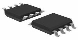
CD4052 4-Channel Multiplexer and Demulitplexer IC: Datasheet, Equivalent and Working


320ns, 150ns SP4T 240Ohm Analog Switches 4052 50nA 16-SOIC (0.154, 3.90mm Width)
The CD4052 is a 4-Channel Multiplexer and Demultiplexer IC. It can either be used as a 4:1 Multiplexer or 1:4 Demultiplexer. This article mainly covers datasheet, equivalents, pin, working, and more details about CD4052 multiplexer. Furthermore, there is a huge range of semiconductors, capacitors, resistors, and ICs in stock. Welcome your RFQ!

CD4052 4x1 multiplexer and demultiplexer Example with proteus simulation
- What is CD4052 Multiplexer?
- CD4052 Multiplexer Pinout
- CD4052 Multiplexer CAD Model
- Specifications
- Features of CD4052 Multiplexer
- Alternatives for CD4052 Multiplexer
- CD4052 Multiplexer Equivalents
- CD4052 Applications
- Where to Use CD4052
- How to Use CD4052
- CD4052 Dimensions
- CD4052 Manufacturer
- Parts with Similar Specs
- Datasheet PDF
What is CD4052 Multiplexer?
The CD4052 is a 4-channel analog/digital dual single-pole switch that can be used in analog or digital 4:1 multiplexer/demultiplexer applications. Each switch has four independent inputs and outputs as well as a common input and output. Both switches have a digital inhibit input (INH) and two digital select inputs (A and B). The switches are turned off when INH is HIGH.
CD4052 Multiplexer Pinout

CD4052 Multiplexer Pinout
| Pin Number | Pin Name | Description |
| 16 | Vdd | Positive power input, maximum 20V |
| 7 | Vee | Negative power rail, normally connected to ground. |
| 8 | Vss (Ground) | Connected to the ground of the circuit |
| 6 | INH | Enable pin – Must be pulled to ground for normal operation |
| 9,10 | A,B | Channel Select pins |
| 1,12 | Y0,X0 | Channel 0 Input / Output |
| 5,14 | Y1,X1 | Channel 1 Input / Output |
| 2,15 | Y2,X2 | Channel 2 Input / Output |
| 4,11 | Y3,X3 | Channel 3 Input / Output |
| 3,13 | Y,X | Common Output / Input |
CD4052 Multiplexer CAD Model

CD4052 Symbol

CD4052 Footprint

CD4052 3D Model
Specifications
- TypeParameter
- Mount
In electronic components, the term "Mount" typically refers to the method or process of physically attaching or fixing a component onto a circuit board or other electronic device. This can involve soldering, adhesive bonding, or other techniques to secure the component in place. The mounting process is crucial for ensuring proper electrical connections and mechanical stability within the electronic system. Different components may have specific mounting requirements based on their size, shape, and function, and manufacturers provide guidelines for proper mounting procedures to ensure optimal performance and reliability of the electronic device.
Surface Mount - Mounting Type
The "Mounting Type" in electronic components refers to the method used to attach or connect a component to a circuit board or other substrate, such as through-hole, surface-mount, or panel mount.
Surface Mount - Package / Case
refers to the protective housing that encases an electronic component, providing mechanical support, electrical connections, and thermal management.
16-SOIC (0.154, 3.90mm Width) - Number of Pins16
- Supplier Device Package
The parameter "Supplier Device Package" in electronic components refers to the physical packaging or housing of the component as provided by the supplier. It specifies the form factor, dimensions, and layout of the component, which are crucial for compatibility and integration into electronic circuits and systems. The supplier device package information typically includes details such as the package type (e.g., DIP, SOP, QFN), number of pins, pitch, and overall size, allowing engineers and designers to select the appropriate component for their specific application requirements. Understanding the supplier device package is essential for proper component selection, placement, and soldering during the manufacturing process to ensure optimal performance and reliability of the electronic system.
16-SOIC - Turn Off Delay Time
It is the time from when Vgs drops below 90% of the gate drive voltage to when the drain current drops below 90% of the load current. It is the delay before current starts to transition in the load, and depends on Rg. Ciss.
420 ns - Operating Temperature
The operating temperature is the range of ambient temperature within which a power supply, or any other electrical equipment, operate in. This ranges from a minimum operating temperature, to a peak or maximum operating temperature, outside which, the power supply may fail.
-55°C~125°C TA - Packaging
Semiconductor package is a carrier / shell used to contain and cover one or more semiconductor components or integrated circuits. The material of the shell can be metal, plastic, glass or ceramic.
Tube - Published2002
- Part Status
Parts can have many statuses as they progress through the configuration, analysis, review, and approval stages.
Obsolete - Moisture Sensitivity Level (MSL)
Moisture Sensitivity Level (MSL) is a standardized rating that indicates the susceptibility of electronic components, particularly semiconductors, to moisture-induced damage during storage and the soldering process, defining the allowable exposure time to ambient conditions before they require special handling or baking to prevent failures
1 (Unlimited) - Resistance
Resistance is a fundamental property of electronic components that measures their opposition to the flow of electric current. It is denoted by the symbol "R" and is measured in ohms (Ω). Resistance is caused by the collisions of electrons with atoms in a material, which generates heat and reduces the flow of current. Components with higher resistance will impede the flow of current more than those with lower resistance. Resistance plays a crucial role in determining the behavior and functionality of electronic circuits, such as limiting current flow, voltage division, and controlling power dissipation.
1.05kOhm - Max Operating Temperature
The Maximum Operating Temperature is the maximum body temperature at which the thermistor is designed to operate for extended periods of time with acceptable stability of its electrical characteristics.
125°C - Min Operating Temperature
The "Min Operating Temperature" parameter in electronic components refers to the lowest temperature at which the component is designed to operate effectively and reliably. This parameter is crucial for ensuring the proper functioning and longevity of the component, as operating below this temperature may lead to performance issues or even damage. Manufacturers specify the minimum operating temperature to provide guidance to users on the environmental conditions in which the component can safely operate. It is important to adhere to this parameter to prevent malfunctions and ensure the overall reliability of the electronic system.
-55°C - Max Power Dissipation
The maximum power that the MOSFET can dissipate continuously under the specified thermal conditions.
500mW - Base Part Number
The "Base Part Number" (BPN) in electronic components serves a similar purpose to the "Base Product Number." It refers to the primary identifier for a component that captures the essential characteristics shared by a group of similar components. The BPN provides a fundamental way to reference a family or series of components without specifying all the variations and specific details.
4052 - Number of Outputs2
- Polarity
In electronic components, polarity refers to the orientation or direction in which the component must be connected in a circuit to function properly. Components such as diodes, capacitors, and LEDs have polarity markings to indicate which terminal should be connected to the positive or negative side of the circuit. Connecting a component with incorrect polarity can lead to malfunction or damage. It is important to pay attention to polarity markings and follow the manufacturer's instructions to ensure proper operation of electronic components.
Non-Inverting - Number of Channels2
- Number of Circuits2
- Max Supply Voltage
In general, the absolute maximum common-mode voltage is VEE-0.3V and VCC+0.3V, but for products without a protection element at the VCC side, voltages up to the absolute maximum rated supply voltage (i.e. VEE+36V) can be supplied, regardless of supply voltage.
15V - Min Supply Voltage
The minimum supply voltage (V min ) is explored for sequential logic circuits by statistically simulating the impact of within-die process variations and gate-dielectric soft breakdown on data retention and hold time.
5V - Nominal Supply Current
Nominal current is the same as the rated current. It is the current drawn by the motor while delivering rated mechanical output at its shaft.
20μA - Power Dissipation
the process by which an electronic or electrical device produces heat (energy loss or waste) as an undesirable derivative of its primary action.
500mW - Throw Configuration
"Throw Configuration" is a term commonly used in the context of switches and relays in electronic components. It refers to the number of positions or states that the switch or relay can be set to. For example, a single-throw (ST) configuration means the switch has only one position, while a double-throw (DT) configuration means the switch has two positions.The throw configuration is important because it determines the versatility and functionality of the switch or relay. Different applications may require different throw configurations to control the flow of current or signals effectively. Understanding the throw configuration of a component is crucial for proper installation and operation within an electronic circuit.
SP4T - Propagation Delay
the flight time of packets over the transmission link and is limited by the speed of light.
55 ns - Turn On Delay Time
Turn-on delay, td(on), is the time taken to charge the input capacitance of the device before drain current conduction can start.
1.2 μs - Logic Function
In electronic components, the term "Logic Function" refers to the specific operation or behavior of a component based on its input signals. It describes how the component processes the input signals to produce the desired output. Logic functions are fundamental to digital circuits and are used to perform logical operations such as AND, OR, NOT, and XOR.Each electronic component, such as logic gates or flip-flops, is designed to perform a specific logic function based on its internal circuitry. By understanding the logic function of a component, engineers can design and analyze complex digital systems to ensure proper functionality and performance. Different logic functions can be combined to create more complex operations, allowing for the creation of sophisticated digital devices and systems.
Demultiplexer, Multiplexer - Number of Inputs8
- Voltage - Supply, Single/Dual (±)
The parameter "Voltage - Supply, Single/Dual (±)" in electronic components refers to the power supply voltage required for the proper operation of the component. This parameter indicates whether the component requires a single power supply voltage (e.g., 5V) or a dual power supply voltage (e.g., ±15V). For components that require a single power supply voltage, only one voltage level is needed for operation. On the other hand, components that require a dual power supply voltage need both positive and negative voltage levels to function correctly.Understanding the voltage supply requirements of electronic components is crucial for designing and integrating them into circuits to ensure proper functionality and prevent damage due to incorrect voltage levels.
5V~15V ±2.5V~7.5V - Supply Type
Supply Type in electronic components refers to the classification of power sources used to operate the component. It indicates whether the component requires DC or AC power, and if DC, specifies the voltage levels such as low, medium, or high. Different supply types can affect the performance, compatibility, and application of the component in electronic circuits. Understanding the supply type is crucial for proper component selection and integration into electronic designs.
Dual, Single - Bandwidth
In electronic components, "Bandwidth" refers to the range of frequencies over which the component can effectively operate or pass signals without significant loss or distortion. It is a crucial parameter for devices like amplifiers, filters, and communication systems. The bandwidth is typically defined as the difference between the upper and lower frequencies at which the component's performance meets specified criteria, such as a certain level of signal attenuation or distortion. A wider bandwidth indicates that the component can handle a broader range of frequencies, making it more versatile for various applications. Understanding the bandwidth of electronic components is essential for designing and optimizing circuits to ensure proper signal transmission and reception within the desired frequency range.
40MHz - Max Dual Supply Voltage
A Dual power supply is a regular direct current power supply. It can provide a positive as well as negative voltage. It ensures stable power supply to the device as well as it helps to prevent system damage.
7.5V - Number of Gates
The number of gates per IC varies depending on the number of inputs per gate. Two?input gates are common, but if only a single input is required, such as in the 744 NOT(or inverter) gates, a 14 pin IC can accommodate 6 (or Hex) gates.
2 - -3db Bandwidth
The "-3dB bandwidth" of an electronic component refers to the frequency range over which the component's output signal power is reduced by 3 decibels (dB) compared to its maximum output power. This parameter is commonly used to describe the frequency response of components such as amplifiers, filters, and other signal processing devices. The -3dB point is significant because it represents the half-power point, where the output signal power is reduced to half of its maximum value. Understanding the -3dB bandwidth is important for designing and analyzing electronic circuits to ensure that signals are accurately processed within the desired frequency range.
40MHz - On-State Resistance (Max)
The "On-State Resistance (Max)" parameter in electronic components refers to the maximum resistance exhibited by the component when it is in the fully conducting state. This resistance is typically measured when the component is carrying the maximum specified current. A lower on-state resistance indicates better conductivity and efficiency of the component when it is in the on-state. It is an important parameter to consider when selecting components for applications where low power dissipation and high efficiency are critical factors.
240Ohm - Min Dual Supply Voltage
The parameter "Min Dual Supply Voltage" in electronic components refers to the minimum voltage required for the proper operation of a device that uses dual power supplies. Dual power supplies typically consist of a positive and a negative voltage source. The "Min Dual Supply Voltage" specification ensures that both the positive and negative supply voltages are within a certain range to guarantee the device functions correctly. It is important to adhere to this parameter to prevent damage to the component and ensure reliable performance.
2.5V - Multiplexer/Demultiplexer Circuit
A Multiplexer/Demultiplexer Circuit is an electronic component used in digital circuits to select one of several input signals and route it to a single output. A multiplexer, also known as a "mux," is used to combine multiple input signals into a single output, while a demultiplexer, also known as a "demux," is used to take a single input and route it to one of several possible outputs. These circuits are commonly used in data transmission, communication systems, and digital signal processing applications to efficiently manage and control the flow of data. Multiplexers and demultiplexers play a crucial role in optimizing the use of resources and improving the overall performance of electronic systems.
4:1 - Current - Leakage (IS(off)) (Max)
Current - Leakage (IS(off)) (Max) refers to the maximum amount of current that flows through a device when it is in its off state, meaning it is not conducting or not intended to be active. This parameter is crucial in determining the efficiency of electronic components, especially in battery-operated devices, as higher leakage currents can lead to increased power consumption and reduced battery life. It is typically measured in microamperes (µA) or milliamperes (mA) and helps engineers assess the suitability of a component for low-power applications.
50nA - Switch Circuit
establishes connections between links, on demand and as available, in order to establish an end-to-end circuit between devices.
SP4T - Switch Time (Ton, Toff) (Max)
The parameter "Switch Time (Ton, Toff) (Max)" in electronic components refers to the maximum time it takes for a device to transition between its on and off states. Ton represents the turn-on time, which is the time taken for the device to switch from the off state to the on state, while Toff represents the turn-off time, which is the time taken for the device to switch from the on state to the off state. This parameter is crucial in determining the speed and efficiency of the device's switching operation. A shorter switch time generally indicates faster switching speeds and better performance of the electronic component.
320ns, 150ns - Channel-to-Channel Matching (ΔRon)
Channel-to-Channel Matching (ΔRon) refers to the variation in the on-resistance of multiple channels within a multi-channel electronic component, such as a multiplexer or a switch. It is a measure of how closely the on-resistance values of different channels match each other. The lower the ΔRon value, the better the matching between channels, which is important for ensuring consistent performance across all channels in a system. Channel-to-Channel Matching is critical in applications where precise and uniform signal processing is required, such as in instrumentation, audio equipment, and communication systems. Manufacturers provide specifications for ΔRon to help designers select components that meet their performance requirements.
5Ohm - REACH SVHC
The parameter "REACH SVHC" in electronic components refers to the compliance with the Registration, Evaluation, Authorization, and Restriction of Chemicals (REACH) regulation regarding Substances of Very High Concern (SVHC). SVHCs are substances that may have serious effects on human health or the environment, and their use is regulated under REACH to ensure their safe handling and minimize their impact.Manufacturers of electronic components need to declare if their products contain any SVHCs above a certain threshold concentration and provide information on the safe use of these substances. This information allows customers to make informed decisions about the potential risks associated with using the components and take appropriate measures to mitigate any hazards.Ensuring compliance with REACH SVHC requirements is essential for electronics manufacturers to meet regulatory standards, protect human health and the environment, and maintain transparency in their supply chain. It also demonstrates a commitment to sustainability and responsible manufacturing practices in the electronics industry.
Unknown - RoHS Status
RoHS means “Restriction of Certain Hazardous Substances” in the “Hazardous Substances Directive” in electrical and electronic equipment.
RoHS Compliant - Lead Free
Lead Free is a term used to describe electronic components that do not contain lead as part of their composition. Lead is a toxic material that can have harmful effects on human health and the environment, so the electronics industry has been moving towards lead-free components to reduce these risks. Lead-free components are typically made using alternative materials such as silver, copper, and tin. Manufacturers must comply with regulations such as the Restriction of Hazardous Substances (RoHS) directive to ensure that their products are lead-free and environmentally friendly.
Lead Free
Features of CD4052 Multiplexer
Wide range of digital and analog signal levels: digital 3 – 15V, analog to 15Vp-p
Low “ON” resistance: 80Ω (typ.) over entire 15Vp-p signal-input range for VDD − VEE = 15V
High “OFF” resistance: channel leakage of ±10 pA (Typ.) at VDD − VEE = 10V
Logic level conversion for digital addressing signals of 3 – 15V (VDD − VSS = 3 – 15V) to switch analog signals to 15 Vp-p (VDD − VEE = 15V)
Matched switch characteristics: ∆RON = 5Ω (Typ.) for VDD − VEE = 15V
Very low quiescent power dissipation under all digital-control input and supply conditions: 1 µ W (typ.) at VDD − VSS = VDD − VEE = 10V
Binary address decoding on chip
Alternatives for CD4052 Multiplexer
74HC4067, 74HC157, CD4016
CD4052 Multiplexer Equivalents
NTE4052, 4017
CD4052 Applications
Multiplexer and Demultiplexer circuit
A/D and D/A converter circuits
Network switching
Programmable Logic circuits
Where to Use CD4052
The CD4052 is a four-channel differential multiplexer/demultiplexer with two binary control inputs A and B. It accepts four inputs from four channels and outputs on channels X, Y, and an inhibit input in multiplexer mode. The two binary input signals A and B control which channels should be switched on.
The CD4052 IC can be used as a demultiplexer as well. It will only accept one input in this mode. The output will be routed to channel 0, 1, 2, or 3 depending on the selection pins A and B. Vss is connected to the circuit's ground, whereas Pin 15 is connected to the power supply. The inhibit pin is in charge of channel enabling and disabling. Channels are enabled when it is used with 0 logic. When the inhibit pin is applied with logic 1, no matter what input is applied on select pins, channels are disabled.
| INH | A | B | CHANNEL SELECTION |
| LOW (0) | 0 | 0 | 0 |
| 0 LOW | 1 | 0 | 1 |
| LOW | 0 | 1 | 2 |
| 0 | 1 | 1 | 3 |
| 1 | X | X | None |
CD4052 Working Truth Table
How to Use CD4052
Use CD4052 as a Multiplexer
It has two channels, X and Y, in multiplexer mode. X0 to X3 for channel X, and Y0 to Y3 for channel Y, are the four inputs for each channel. X and Y are the output pins for both channels. For both 4 cross 1 muxes, input pins A and B serve as common selection lines. These selection lines determine which input signal is shown on the output pin.
This is a working circuit diagram. We are getting output on X and Y pins according to the above table. You may also experiment with it with Proteus. As you can see, pins A and B on the selection line are equal to one. Multiplexer chooses X3 and Y3 inputs based on the selection lines. As a result, these inputs appear on output pins like X and Y.

CD4052 Multiplexer Circuit
Use CD4052 as a Demux
This ic can also be used as a 14 multiplexer. It's also known as a decoder. X and Y are used as input pins in this setup. X0-X3 and Y0-Y3 on the other hand, use an output pin for X and Y, respectively. The selection pins A and B determine which pin output will be shown. As a result, based on digital logic on selected lines A and B, output pins will be X1, Y1 or X2, Y2 or X3, Y3 or X0, Y0.
The functioning principle of the demux is depicted in this simulation figure. As you can see in the figure, input X=1 and input Y=1 are both equal to zero, as are selection lines A and B. As a result, input signals appear on X0 and Y0. In other words, we can modify the values of the selection line signal to change the output.

CD4052 Demux Circuit
CD4052 Dimensions

CD4052 Dimensions
CD4052 Manufacturer
On Semiconductor (Nasdaq: ON) is a manufacturer engaging itself in reducing energy use. It features a comprehensive portfolio of power, signal management, and logic, custom solutions that are energy efficient. It acts as a world-class supply chain with high reliability and a network of manufacturing facilities, sales, offices, and design centers in key markets through North America, Europe, and the Asia Pacific regions.
Parts with Similar Specs
- ImagePart NumberManufacturerPackage / CaseNumber of InputsNumber of PinsLogic FunctionMin Dual Supply VoltageMin Supply VoltageMax Dual Supply VoltageMax Supply VoltageView Compare
![CD4052BCM]()
CD4052BCM
16-SOIC (0.154, 3.90mm Width)
8
16
Demultiplexer, Multiplexer
2.5 V
5 V
7.5 V
15 V
![SP232ACN-L]()
16-SOIC (0.154, 3.90mm Width)
-
16
-
-
4.5 V
-
5.5 V
![TS5V330CDR]()
SOIC
-
20
Receiver, Transceiver
-
4.5 V
-
15 V
![GD75232DWE4]()
SOIC
-
16
Transceiver
-
4.5 V
-
5.5 V


Datasheet PDF
- Datasheets :
- ReachStatement :
What is the use of CD4052?
CD4052 is a dual 4-channel IC that can be used as both a 4:1 multiplexer and 1:4 demultiplexer. It is a CMOS logic-based IC belonging to a CD4000 series of integrated circuits. We can use this IC in both digital and analog applications. In other words, it works for both analog and digital voltage levels.
How does CD4052 work?
CD4052 is a dual 4-channel differential multiplexer/demultiplexer IC with two binary control inputs A and B. Multiplexer mode takes 4 inputs from 4 channels and returns the output on channels X, Y. and an inhibit input.
What is the working principle of CD4052?
CD4052 is a differential 4-channel digitally controlled analog switch with two binary control inputs A and B and INH input. It has low on-resistance and a very low off-leakage current. A digital signal with an amplitude of 4.5-20V can control an analog signal with a peak-to-peak value of 20V.
What is the difference between CD4052 and CD4053?
4052----Dual 4 out of 1 analog switch.
4053----Three 2 out of 1 analog switch.
 2N5087 PNP Transistor: Pinout, Datasheet, and Uses
18 August 20213521
 A Comprehensive Overview of the Analog Devices Inc. 5962-8777101MCA Linear Amplifier
06 March 2024164
 BNO055 Orientation Sensor: Datasheet, Pinout and Features
23 July 20219439
 ATSAMD21G18 Microcontroller: Datasheet, Pinout and Applications
24 August 20217880
 AD831 500 MHz Active Mixer: High Dynamic Range Datasheet & Performance Review
13 March 2026156
 IRL520 Power MOSFET: DV/DT, Vishay, IRL520 Datasheet
30 December 20212532
![MB10F Bridge Stack: Features, Pinout, and Datasheet [Video&FAQ]](https://res.utmel.com/Images/Article/be2ec37f-a7df-40ce-9d94-173c34202fdf.png) MB10F Bridge Stack: Features, Pinout, and Datasheet [Video&FAQ]
MB10F Bridge Stack: Features, Pinout, and Datasheet [Video&FAQ]08 October 202125449
 MC34064 Undervoltage Sensing Circuit: Pinout, Features and Datasheet
04 March 20221368
 Vision Capabilities Are at the Heart of AI's Evolutionary Possession of Intelligence
06 July 20222255
 What is a Memory Controller?
12 August 202033717
 Apple M1 Ultra -- The Technology Behind the Chip Interconnection
12 March 20226926
 What are Weight Sensors?
31 October 202517455
 Towards an Optoelectronic Chip That Mimics the Human Brain
20 April 2022903
 Reverse Voltage Protection for Battery Chargers
29 March 20224955
 New Technology Helps Detect and Prevent Automated Browsing
13 November 20232560
 Introduction to UFS (Universal Flash Storage)
23 July 20218109
ON Semiconductor
In Stock: 14
United States
China
Canada
Japan
Russia
Germany
United Kingdom
Singapore
Italy
Hong Kong(China)
Taiwan(China)
France
Korea
Mexico
Netherlands
Malaysia
Austria
Spain
Switzerland
Poland
Thailand
Vietnam
India
United Arab Emirates
Afghanistan
Åland Islands
Albania
Algeria
American Samoa
Andorra
Angola
Anguilla
Antigua & Barbuda
Argentina
Armenia
Aruba
Australia
Azerbaijan
Bahamas
Bahrain
Bangladesh
Barbados
Belarus
Belgium
Belize
Benin
Bermuda
Bhutan
Bolivia
Bonaire, Sint Eustatius and Saba
Bosnia & Herzegovina
Botswana
Brazil
British Indian Ocean Territory
British Virgin Islands
Brunei
Bulgaria
Burkina Faso
Burundi
Cabo Verde
Cambodia
Cameroon
Cayman Islands
Central African Republic
Chad
Chile
Christmas Island
Cocos (Keeling) Islands
Colombia
Comoros
Congo
Congo (DRC)
Cook Islands
Costa Rica
Côte d’Ivoire
Croatia
Cuba
Curaçao
Cyprus
Czechia
Denmark
Djibouti
Dominica
Dominican Republic
Ecuador
Egypt
El Salvador
Equatorial Guinea
Eritrea
Estonia
Eswatini
Ethiopia
Falkland Islands
Faroe Islands
Fiji
Finland
French Guiana
French Polynesia
Gabon
Gambia
Georgia
Ghana
Gibraltar
Greece
Greenland
Grenada
Guadeloupe
Guam
Guatemala
Guernsey
Guinea
Guinea-Bissau
Guyana
Haiti
Honduras
Hungary
Iceland
Indonesia
Iran
Iraq
Ireland
Isle of Man
Israel
Jamaica
Jersey
Jordan
Kazakhstan
Kenya
Kiribati
Kosovo
Kuwait
Kyrgyzstan
Laos
Latvia
Lebanon
Lesotho
Liberia
Libya
Liechtenstein
Lithuania
Luxembourg
Macao(China)
Madagascar
Malawi
Maldives
Mali
Malta
Marshall Islands
Martinique
Mauritania
Mauritius
Mayotte
Micronesia
Moldova
Monaco
Mongolia
Montenegro
Montserrat
Morocco
Mozambique
Myanmar
Namibia
Nauru
Nepal
New Caledonia
New Zealand
Nicaragua
Niger
Nigeria
Niue
Norfolk Island
North Korea
North Macedonia
Northern Mariana Islands
Norway
Oman
Pakistan
Palau
Palestinian Authority
Panama
Papua New Guinea
Paraguay
Peru
Philippines
Pitcairn Islands
Portugal
Puerto Rico
Qatar
Réunion
Romania
Rwanda
Samoa
San Marino
São Tomé & Príncipe
Saudi Arabia
Senegal
Serbia
Seychelles
Sierra Leone
Sint Maarten
Slovakia
Slovenia
Solomon Islands
Somalia
South Africa
South Sudan
Sri Lanka
St Helena, Ascension, Tristan da Cunha
St. Barthélemy
St. Kitts & Nevis
St. Lucia
St. Martin
St. Pierre & Miquelon
St. Vincent & Grenadines
Sudan
Suriname
Svalbard & Jan Mayen
Sweden
Syria
Tajikistan
Tanzania
Timor-Leste
Togo
Tokelau
Tonga
Trinidad & Tobago
Tunisia
Turkey
Turkmenistan
Turks & Caicos Islands
Tuvalu
U.S. Outlying Islands
U.S. Virgin Islands
Uganda
Ukraine
Uruguay
Uzbekistan
Vanuatu
Vatican City
Venezuela
Wallis & Futuna
Yemen
Zambia
Zimbabwe
![MC14051BDR2G]() MC14051BDR2G
MC14051BDR2GON Semiconductor
![NLAS4599DFT2G]() NLAS4599DFT2G
NLAS4599DFT2GON Semiconductor
![MC74HC4066ADR2G]() MC74HC4066ADR2G
MC74HC4066ADR2GON Semiconductor
![NLAS4157DFT2G]() NLAS4157DFT2G
NLAS4157DFT2GON Semiconductor
![FSA4157P6X]() FSA4157P6X
FSA4157P6XON Semiconductor
![MC14051BDTR2G]() MC14051BDTR2G
MC14051BDTR2GON Semiconductor
![MC74HC4051ADR2G]() MC74HC4051ADR2G
MC74HC4051ADR2GON Semiconductor
![FSA2257MUX]() FSA2257MUX
FSA2257MUXON Semiconductor
![FSA5157P6X]() FSA5157P6X
FSA5157P6XON Semiconductor
![FSA4157AP6X]() FSA4157AP6X
FSA4157AP6XON Semiconductor


