
 Product
 Brand
Brand Articles
 Tools
Tools
AD625: High-Performance Instrumentation Amplifier for Precise Signal Conditioning


50nA 70 dB Instrumentational OP Amps ±18V AD625 20 Pins 20-CLCC
The AD625 is a high-performance instrumentation amplifier designed by Analog Devices Inc. It offers precise signal conditioning and amplification for a wide range of applications. With its excellent features and versatile design, the AD625 is a reliable choice for engineers requiring accurate and reliable signal processing.
Product Introduction
The AD625 is a versatile instrumentation amplifier that provides high-precision signal conditioning. It is designed to accurately amplify small differential input signals while rejecting common-mode noise. The amplifier operates over a wide temperature range of -55°C to 125°C, making it suitable for various environments.
2. Features:
- High common-mode rejection ratio (CMRR) of 70 dB ensures accurate signal amplification even in the presence of common-mode noise.
- Low input offset voltage of 50μV minimizes errors in signal conditioning.
- Wide gain range from 1 to 10 allows for flexible signal amplification.
- High gain bandwidth product of 25 MHz enables the amplifier to handle high-frequency signals.
- Low power consumption of 5mA makes it suitable for battery-powered applications.
- Surface-mount package with 20 pins provides easy integration into PCB designs.
3. Applications:
The AD625 finds applications in various fields where precise signal conditioning and amplification are required. Some primary applications include:
- Medical Equipment: The AD625 is ideal for medical devices such as ECG (electrocardiogram) machines, patient monitoring systems, and bioimpedance measurement equipment. Its high accuracy and low noise characteristics make it suitable for amplifying weak biological signals.
- Industrial Automation: In industrial automation, the AD625 can be used for sensor signal conditioning, strain gauge amplification, and bridge measurements. Its high CMRR and low input offset voltage ensure accurate measurement and control of industrial processes.
- Test and Measurement: The amplifier is well-suited for test and measurement equipment, including data acquisition systems, oscilloscopes, and signal generators. Its wide gain range and high gain bandwidth product enable accurate signal amplification and analysis.
Secondary applications of the AD625 include audio amplification, precision instrumentation, and communication systems. The amplifier can be used in combination with specific modules such as filters, ADCs (analog-to-digital converters), and DACs (digital-to-analog converters) to create comprehensive signal processing solutions.
4. Reference Designs:
Analog Devices Inc. provides several reference designs that utilize the AD625 amplifier. These reference designs serve as a starting point for engineers looking to implement the amplifier in their applications. Some notable reference designs include:
- Precision Signal Conditioning for Data Acquisition: This reference design showcases the AD625's capabilities in accurately conditioning and amplifying small signals for data acquisition systems.
- ECG Signal Conditioning: This reference design demonstrates the use of the AD625 in amplifying ECG signals with high accuracy and low noise.
- Strain Gauge Amplification: This design highlights the AD625's suitability for strain gauge amplification in industrial applications.
5. Alternative Parts:
In case the AD625 is not available or does not meet specific requirements, engineers can consider alternative parts from other manufacturers. Some alternative parts that offer similar functionality include:
- Texas Instruments INA128: This instrumentation amplifier offers high accuracy and low noise performance for precise signal conditioning.
- Maxim Integrated MAX4209: The MAX4209 is a low-power instrumentation amplifier with low input offset voltage and high CMRR.
- Linear Technology LT1167: The LT1167 is a high-performance instrumentation amplifier with low noise and high gain accuracy.
6. FAQs:
Q: Can the AD625 operate in harsh environments?
A: Yes, the AD625 is designed to operate over a wide temperature range of -55°C to 125°C, making it suitable for harsh environments.
Q: What is the maximum supply voltage for the AD625?
A: The AD625 can handle a supply voltage of up to ±18V.
Q: Is the AD625 RoHS compliant?
A: No, the AD625 is not RoHS compliant and contains lead.
Q: What is the maximum gain of the AD625?
A: The AD625 has a maximum gain of 10.
Q: Can the AD625 be used in battery-powered applications?
A: Yes, the AD625 has a low power consumption of 5mA, making it suitable for battery-powered applications.
In conclusion, the AD625 is a high-performance instrumentation amplifier that offers precise signal conditioning and amplification for a wide range of applications. Its excellent features, versatile design, and compatibility with various modules make it a reliable choice for engineers requiring accurate and reliable signal processing.
Specifications
- TypeParameter
- Lifecycle Status
Lifecycle Status refers to the current stage of an electronic component in its product life cycle, indicating whether it is active, obsolete, or transitioning between these states. An active status means the component is in production and available for purchase. An obsolete status indicates that the component is no longer being manufactured or supported, and manufacturers typically provide a limited time frame for support. Understanding the lifecycle status is crucial for design engineers to ensure continuity and reliability in their projects.
PRODUCTION (Last Updated: 2 weeks ago) - Factory Lead Time12 Weeks
- Contact Plating
Contact plating (finish) provides corrosion protection for base metals and optimizes the mechanical and electrical properties of the contact interfaces.
Gold - Mount
In electronic components, the term "Mount" typically refers to the method or process of physically attaching or fixing a component onto a circuit board or other electronic device. This can involve soldering, adhesive bonding, or other techniques to secure the component in place. The mounting process is crucial for ensuring proper electrical connections and mechanical stability within the electronic system. Different components may have specific mounting requirements based on their size, shape, and function, and manufacturers provide guidelines for proper mounting procedures to ensure optimal performance and reliability of the electronic device.
Surface Mount - Mounting Type
The "Mounting Type" in electronic components refers to the method used to attach or connect a component to a circuit board or other substrate, such as through-hole, surface-mount, or panel mount.
Surface Mount - Package / Case
refers to the protective housing that encases an electronic component, providing mechanical support, electrical connections, and thermal management.
20-CLCC - Number of Pins20
- Number of Elements5
- Usage LevelMilitary grade
- Operating Temperature
The operating temperature is the range of ambient temperature within which a power supply, or any other electrical equipment, operate in. This ranges from a minimum operating temperature, to a peak or maximum operating temperature, outside which, the power supply may fail.
-55°C~125°C - Packaging
Semiconductor package is a carrier / shell used to contain and cover one or more semiconductor components or integrated circuits. The material of the shell can be metal, plastic, glass or ceramic.
Tube - JESD-609 Code
The "JESD-609 Code" in electronic components refers to a standardized marking code that indicates the lead-free solder composition and finish of electronic components for compliance with environmental regulations.
e0 - Pbfree Code
The "Pbfree Code" parameter in electronic components refers to the code or marking used to indicate that the component is lead-free. Lead (Pb) is a toxic substance that has been widely used in electronic components for many years, but due to environmental concerns, there has been a shift towards lead-free alternatives. The Pbfree Code helps manufacturers and users easily identify components that do not contain lead, ensuring compliance with regulations and promoting environmentally friendly practices. It is important to pay attention to the Pbfree Code when selecting electronic components to ensure they meet the necessary requirements for lead-free applications.
no - Part Status
Parts can have many statuses as they progress through the configuration, analysis, review, and approval stages.
Active - Moisture Sensitivity Level (MSL)
Moisture Sensitivity Level (MSL) is a standardized rating that indicates the susceptibility of electronic components, particularly semiconductors, to moisture-induced damage during storage and the soldering process, defining the allowable exposure time to ambient conditions before they require special handling or baking to prevent failures
2 (1 Year) - Number of Terminations20
- ECCN Code
An ECCN (Export Control Classification Number) is an alphanumeric code used by the U.S. Bureau of Industry and Security to identify and categorize electronic components and other dual-use items that may require an export license based on their technical characteristics and potential for military use.
EAR99 - Resistance
Resistance is a fundamental property of electronic components that measures their opposition to the flow of electric current. It is denoted by the symbol "R" and is measured in ohms (Ω). Resistance is caused by the collisions of electrons with atoms in a material, which generates heat and reduces the flow of current. Components with higher resistance will impede the flow of current more than those with lower resistance. Resistance plays a crucial role in determining the behavior and functionality of electronic circuits, such as limiting current flow, voltage division, and controlling power dissipation.
1GOhm - Terminal Finish
Terminal Finish refers to the surface treatment applied to the terminals or leads of electronic components to enhance their performance and longevity. It can improve solderability, corrosion resistance, and overall reliability of the connection in electronic assemblies. Common finishes include nickel, gold, and tin, each possessing distinct properties suitable for various applications. The choice of terminal finish can significantly impact the durability and effectiveness of electronic devices.
Tin/Lead (Sn/Pb) - Max Power Dissipation
The maximum power that the MOSFET can dissipate continuously under the specified thermal conditions.
450mW - Terminal Position
In electronic components, the term "Terminal Position" refers to the physical location of the connection points on the component where external electrical connections can be made. These connection points, known as terminals, are typically used to attach wires, leads, or other components to the main body of the electronic component. The terminal position is important for ensuring proper connectivity and functionality of the component within a circuit. It is often specified in technical datasheets or component specifications to help designers and engineers understand how to properly integrate the component into their circuit designs.
QUAD - Terminal Form
Occurring at or forming the end of a series, succession, or the like; closing; concluding.
NO LEAD - Peak Reflow Temperature (Cel)
Peak Reflow Temperature (Cel) is a parameter that specifies the maximum temperature at which an electronic component can be exposed during the reflow soldering process. Reflow soldering is a common method used to attach electronic components to a circuit board. The Peak Reflow Temperature is crucial because it ensures that the component is not damaged or degraded during the soldering process. Exceeding the specified Peak Reflow Temperature can lead to issues such as component failure, reduced performance, or even permanent damage to the component. It is important for manufacturers and assemblers to adhere to the recommended Peak Reflow Temperature to ensure the reliability and functionality of the electronic components.
NOT APPLICABLE - Number of Functions1
- Supply Voltage
Supply voltage refers to the electrical potential difference provided to an electronic component or circuit. It is crucial for the proper operation of devices, as it powers their functions and determines performance characteristics. The supply voltage must be within specified limits to ensure reliability and prevent damage to components. Different electronic devices have specific supply voltage requirements, which can vary widely depending on their design and intended application.
15V - Reach Compliance Code
Reach Compliance Code refers to a designation indicating that electronic components meet the requirements set by the Registration, Evaluation, Authorization, and Restriction of Chemicals (REACH) regulation in the European Union. It signifies that the manufacturer has assessed and managed the chemical substances within the components to ensure safety and environmental protection. This code is vital for compliance with regulations aimed at minimizing risks associated with hazardous substances in electronic products.
not_compliant - Time@Peak Reflow Temperature-Max (s)
Time@Peak Reflow Temperature-Max (s) refers to the maximum duration that an electronic component can be exposed to the peak reflow temperature during the soldering process, which is crucial for ensuring reliable solder joint formation without damaging the component.
NOT APPLICABLE - Base Part Number
The "Base Part Number" (BPN) in electronic components serves a similar purpose to the "Base Product Number." It refers to the primary identifier for a component that captures the essential characteristics shared by a group of similar components. The BPN provides a fundamental way to reference a family or series of components without specifying all the variations and specific details.
AD625 - Pin Count
a count of all of the component leads (or pins)
20 - Qualification Status
An indicator of formal certification of qualifications.
Not Qualified - Number of Circuits1
- Power Dissipation
the process by which an electronic or electrical device produces heat (energy loss or waste) as an undesirable derivative of its primary action.
450mW - Current - Supply
Current - Supply is a parameter in electronic components that refers to the maximum amount of electrical current that the component can provide to the circuit it is connected to. It is typically measured in units of amperes (A) and is crucial for determining the power handling capability of the component. Understanding the current supply rating is important for ensuring that the component can safely deliver the required current without overheating or failing. It is essential to consider this parameter when designing circuits to prevent damage to the component and ensure proper functionality of the overall system.
5mA - Slew Rate
the maximum rate of output voltage change per unit time.
5V/μs - Amplifier Type
Amplifier Type refers to the classification or categorization of amplifiers based on their design, functionality, and characteristics. Amplifiers are electronic devices that increase the amplitude of a signal, such as voltage or current. The type of amplifier determines its specific application, performance capabilities, and operating characteristics. Common types of amplifiers include operational amplifiers (op-amps), power amplifiers, audio amplifiers, and radio frequency (RF) amplifiers. Understanding the amplifier type is crucial for selecting the right component for a particular circuit or system design.
Instrumentation - Common Mode Rejection Ratio
Common Mode Rejection Ratio (CMRR) is a measure of the ability of a differential amplifier to reject input signals that are common to both input terminals. It is defined as the ratio of the differential gain to the common mode gain. A high CMRR indicates that the amplifier can effectively eliminate noise and interference that affects both inputs simultaneously, enhancing the fidelity of the amplified signal. CMRR is typically expressed in decibels (dB), with higher values representing better performance in rejecting common mode signals.
70 dB - Current - Input Bias
The parameter "Current - Input Bias" in electronic components refers to the amount of current required at the input terminal of a device to maintain proper operation. It is a crucial specification as it determines the minimum input current needed for the component to function correctly. Input bias current can affect the performance and accuracy of the device, especially in precision applications where small signal levels are involved. It is typically specified in datasheets for operational amplifiers, transistors, and other semiconductor devices to provide users with important information for circuit design and analysis.
50nA - Voltage - Supply, Single/Dual (±)
The parameter "Voltage - Supply, Single/Dual (±)" in electronic components refers to the power supply voltage required for the proper operation of the component. This parameter indicates whether the component requires a single power supply voltage (e.g., 5V) or a dual power supply voltage (e.g., ±15V). For components that require a single power supply voltage, only one voltage level is needed for operation. On the other hand, components that require a dual power supply voltage need both positive and negative voltage levels to function correctly.Understanding the voltage supply requirements of electronic components is crucial for designing and integrating them into circuits to ensure proper functionality and prevent damage due to incorrect voltage levels.
±18V - Input Offset Voltage (Vos)
Input Offset Voltage (Vos) is a key parameter in electronic components, particularly in operational amplifiers. It refers to the voltage difference that must be applied between the two input terminals of the amplifier to nullify the output voltage when the input terminals are shorted together. In simpler terms, it represents the voltage required to bring the output of the amplifier to zero when there is no input signal present. Vos is an important parameter as it can introduce errors in the output signal of the amplifier, especially in precision applications where accuracy is crucial. Minimizing Vos is essential to ensure the amplifier operates with high precision and accuracy.
50μV - Gain Bandwidth Product
The gain–bandwidth product (designated as GBWP, GBW, GBP, or GB) for an amplifier is the product of the amplifier's bandwidth and the gain at which the bandwidth is measured.
25MHz - Neg Supply Voltage-Nom (Vsup)
The parameter "Neg Supply Voltage-Nom (Vsup)" in electronic components refers to the nominal negative supply voltage that the component requires to operate within its specified performance characteristics. This parameter indicates the minimum voltage level that must be provided to the component's negative supply pin for proper functionality. It is important to ensure that the negative supply voltage provided to the component does not exceed the maximum specified value to prevent damage or malfunction. Understanding and adhering to the specified negative supply voltage requirements is crucial for the reliable operation of the electronic component in a circuit.
-15V - Voltage - Input Offset
Voltage - Input Offset is a parameter that refers to the difference in voltage between the input terminals of an electronic component, such as an operational amplifier, when the input voltage is zero. It is an important characteristic that can affect the accuracy and performance of the component in various applications. A low input offset voltage is desirable as it indicates that the component will have minimal error in its output when the input signal is near zero. Manufacturers typically provide this specification in the component's datasheet to help users understand the component's behavior and make informed decisions when designing circuits.
200μV - -3db Bandwidth
The "-3dB bandwidth" of an electronic component refers to the frequency range over which the component's output signal power is reduced by 3 decibels (dB) compared to its maximum output power. This parameter is commonly used to describe the frequency response of components such as amplifiers, filters, and other signal processing devices. The -3dB point is significant because it represents the half-power point, where the output signal power is reduced to half of its maximum value. Understanding the -3dB bandwidth is important for designing and analyzing electronic circuits to ensure that signals are accurately processed within the desired frequency range.
0.65MHz - Screening Level
In electronic components, the term "Screening Level" refers to the level of testing and inspection that a component undergoes to ensure its reliability and performance. This process involves subjecting the component to various tests, such as temperature cycling, burn-in, and electrical testing, to identify any defects or weaknesses that could affect its functionality. The screening level is typically determined based on the application requirements and the criticality of the component in the system. Components that undergo higher screening levels are generally more reliable but may also be more expensive. Overall, the screening level helps to ensure that electronic components meet the necessary quality standards for their intended use.
MIL-STD-883 Class B - Voltage Gain-Min
Voltage Gain-Min is a parameter used to describe the minimum amplification factor of an electronic component, such as an amplifier or transistor. It represents the smallest amount by which the input voltage signal is amplified to produce the output voltage signal. A higher Voltage Gain-Min value indicates a greater amplification capability of the component. This parameter is crucial in determining the performance and efficiency of electronic circuits, as it directly influences the signal strength and quality of the output. Manufacturers provide this specification to help engineers and designers select the appropriate components for their specific application requirements.
1 - Voltage Gain-Nom
Voltage Gain-Nom is a parameter used to describe the ratio of the output voltage to the input voltage in electronic components such as amplifiers. It represents the amplification factor of the component and indicates how much the input voltage is amplified to produce the output voltage. The "Nom" in the term signifies that this value is the nominal or typical voltage gain under specified operating conditions. A higher voltage gain indicates a greater amplification of the input signal, while a lower voltage gain signifies less amplification. This parameter is crucial in determining the performance and functionality of electronic circuits and devices.
10 - Length8.89mm
- RoHS Status
RoHS means “Restriction of Certain Hazardous Substances” in the “Hazardous Substances Directive” in electrical and electronic equipment.
Non-RoHS Compliant - Lead Free
Lead Free is a term used to describe electronic components that do not contain lead as part of their composition. Lead is a toxic material that can have harmful effects on human health and the environment, so the electronics industry has been moving towards lead-free components to reduce these risks. Lead-free components are typically made using alternative materials such as silver, copper, and tin. Manufacturers must comply with regulations such as the Restriction of Hazardous Substances (RoHS) directive to ensure that their products are lead-free and environmentally friendly.
Contains Lead
Parts with Similar Specs
- ImagePart NumberManufacturerPackage / CaseNumber of PinsNumber of CircuitsSlew RateGain Bandwidth ProductInput Offset Voltage (Vos)Common Mode Rejection RatioSupply VoltageView Compare
![5962-87719012A]()
5962-87719012A
20-CLCC
20
1
5V/μs
25MHz
50 μV
70 dB
15 V
![5962-9460202Q2A]()
20-CLCC
20
1
5V/μs
25MHz
200 μV
90 dB
15 V
![AD524SE/883B]()
20-CLCC
20
1
5V/μs
1MHz
250 μV
90 dB
15 V
![LM158FKB]()
LCC
20
-
0.3 V/μs
700 kHz
5 mV
70 dB
5 V
![AD625SE/883B]()
LCC
20
-
35 V/μs
9.4 MHz
6 mV
70 dB
5 V


Datasheet PDF
- Datasheets :
- PCN Assembly/Origin :
- ConflictMineralStatement :
 MMBT2907A PNP Transistor: 60V 0.8A, SOT-23 MMBT2907A Bipolar Transistor and Datasheet pdf
20 January 20222468
 STM8S005K6T6C Microcontroller: Features, Applications and Datasheet
27 December 20232244
 LM5166DRCR: Datasheet, Pinout, 10-VFDFN, high efficiency
12 February 2022952
 How to use BME280 with Arduino?
07 June 20223902
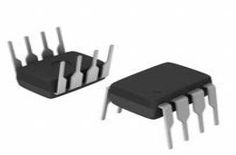 LF353N Dual JFET Input Op-Amp: Datasheet, Pinout and Equivalents
15 September 202112547
![RG8 VS LMR400[FAQ]: Differentiate the differences between them.](https://res.utmel.com/Images/Article/001960bf-022b-4557-968e-67dcf2b7c44f.png) RG8 VS LMR400[FAQ]: Differentiate the differences between them.
RG8 VS LMR400[FAQ]: Differentiate the differences between them.12 June 202422850
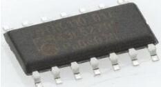 HEF4094BT Shift Register: Pinout, Datasheet, Functional Diagram
16 February 20226358
 Comprehensive Guide to XC7Z010-1CLG400C Specifications and Features
21 February 20251388
 Semiconductor Market Poised for Strong Rebound in 2024, Predicts WSTS
11 December 20235180
 Introduction to the Types of Monitor Cables
01 April 202416631
 Surge Protector Best Practices for Everyday Use
10 July 20252217
 Ultimate Guide to KVM Switches: Definition, Usage, and 2025 Trends
18 December 202512799
 What is Wi-Fi 7?
20 August 20215732
 Active Electroacoustic Resonator-Silent Speaker
10 November 20215791
 nF Capacitors: Definition, Conversion, Circuit Applications, and Selection
12 August 20257510
 Designing a GaN-based Dual Active Bridge for PHEV Chargers
17 May 20242411
Analog Devices Inc.
In Stock: 1502
United States
China
Canada
Japan
Russia
Germany
United Kingdom
Singapore
Italy
Hong Kong(China)
Taiwan(China)
France
Korea
Mexico
Netherlands
Malaysia
Austria
Spain
Switzerland
Poland
Thailand
Vietnam
India
United Arab Emirates
Afghanistan
Åland Islands
Albania
Algeria
American Samoa
Andorra
Angola
Anguilla
Antigua & Barbuda
Argentina
Armenia
Aruba
Australia
Azerbaijan
Bahamas
Bahrain
Bangladesh
Barbados
Belarus
Belgium
Belize
Benin
Bermuda
Bhutan
Bolivia
Bonaire, Sint Eustatius and Saba
Bosnia & Herzegovina
Botswana
Brazil
British Indian Ocean Territory
British Virgin Islands
Brunei
Bulgaria
Burkina Faso
Burundi
Cabo Verde
Cambodia
Cameroon
Cayman Islands
Central African Republic
Chad
Chile
Christmas Island
Cocos (Keeling) Islands
Colombia
Comoros
Congo
Congo (DRC)
Cook Islands
Costa Rica
Côte d’Ivoire
Croatia
Cuba
Curaçao
Cyprus
Czechia
Denmark
Djibouti
Dominica
Dominican Republic
Ecuador
Egypt
El Salvador
Equatorial Guinea
Eritrea
Estonia
Eswatini
Ethiopia
Falkland Islands
Faroe Islands
Fiji
Finland
French Guiana
French Polynesia
Gabon
Gambia
Georgia
Ghana
Gibraltar
Greece
Greenland
Grenada
Guadeloupe
Guam
Guatemala
Guernsey
Guinea
Guinea-Bissau
Guyana
Haiti
Honduras
Hungary
Iceland
Indonesia
Iran
Iraq
Ireland
Isle of Man
Israel
Jamaica
Jersey
Jordan
Kazakhstan
Kenya
Kiribati
Kosovo
Kuwait
Kyrgyzstan
Laos
Latvia
Lebanon
Lesotho
Liberia
Libya
Liechtenstein
Lithuania
Luxembourg
Macao(China)
Madagascar
Malawi
Maldives
Mali
Malta
Marshall Islands
Martinique
Mauritania
Mauritius
Mayotte
Micronesia
Moldova
Monaco
Mongolia
Montenegro
Montserrat
Morocco
Mozambique
Myanmar
Namibia
Nauru
Nepal
New Caledonia
New Zealand
Nicaragua
Niger
Nigeria
Niue
Norfolk Island
North Korea
North Macedonia
Northern Mariana Islands
Norway
Oman
Pakistan
Palau
Palestinian Authority
Panama
Papua New Guinea
Paraguay
Peru
Philippines
Pitcairn Islands
Portugal
Puerto Rico
Qatar
Réunion
Romania
Rwanda
Samoa
San Marino
São Tomé & Príncipe
Saudi Arabia
Senegal
Serbia
Seychelles
Sierra Leone
Sint Maarten
Slovakia
Slovenia
Solomon Islands
Somalia
South Africa
South Sudan
Sri Lanka
St Helena, Ascension, Tristan da Cunha
St. Barthélemy
St. Kitts & Nevis
St. Lucia
St. Martin
St. Pierre & Miquelon
St. Vincent & Grenadines
Sudan
Suriname
Svalbard & Jan Mayen
Sweden
Syria
Tajikistan
Tanzania
Timor-Leste
Togo
Tokelau
Tonga
Trinidad & Tobago
Tunisia
Turkey
Turkmenistan
Turks & Caicos Islands
Tuvalu
U.S. Outlying Islands
U.S. Virgin Islands
Uganda
Ukraine
Uruguay
Uzbekistan
Vanuatu
Vatican City
Venezuela
Wallis & Futuna
Yemen
Zambia
Zimbabwe
![AD826AR-REEL7]() AD826AR-REEL7
AD826AR-REEL7Analog Devices Inc.
![AD8062ARM]() AD8062ARM
AD8062ARMAnalog Devices Inc.
![AD8532ARU-REEL]() AD8532ARU-REEL
AD8532ARU-REELAnalog Devices Inc.
![OP113ES]() OP113ES
OP113ESAnalog Devices Inc.
![SSM2142P]() SSM2142P
SSM2142PAnalog Devices, Inc.
![LTC1050CS8]() LTC1050CS8
LTC1050CS8Linear Technology/Analog Devices
![AMP02EPZ]() AMP02EPZ
AMP02EPZAnalog Devices Inc.
![AD822ARZ-REEL7]() AD822ARZ-REEL7
AD822ARZ-REEL7Analog Devices Inc.
![OP2177ARZ-REEL7]() OP2177ARZ-REEL7
OP2177ARZ-REEL7Analog Devices Inc.
![AD8066ARZ-R7]() AD8066ARZ-R7
AD8066ARZ-R7Analog Devices Inc.


