
 Product
 Brand
Brand Articles
 Tools
Tools
CD4066B Bilateral Switch: Features, Speicifications and Applications

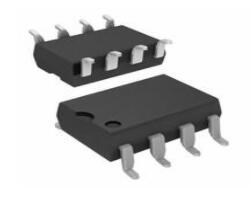
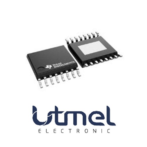
14 Terminations 3V~18V 14 Pin CD4066 Signal switch 4000B Series 2 Outputs 4 Functions


14 Terminations 3V~18V 14 Pin CD4066 Signal switch 4000B Series 2 Outputs 4 Functions
The CD4066B device is a quad bilateral switch intended for the transmission or multiplexing of analog or digital signals. It is pin-for-pin compatible with the CD4016B device, but exhibits a much lower on-state resistance. In addition, the on-state resistance is relatively constant over the full signalinput range.
CD4066B Description
The CD4066B device is a quad bilateral switch intended for the transmission or multiplexing of analog or digital signals. It is pin-for-pin compatible with the CD4016B device, but exhibits a much lower on-state resistance. In addition, the on-state resistance is relatively constant over the full signalinput range. The CD4066B device consists of four bilateral switches, each with independent controls. Both the p and the n devices in a given switch are biased on or off simultaneously by the control signal. As shown in Figure below, the well of the n-channel device on each switch is tied to either the input (when the switch is on) or to VSS (when the switch is off). This configuration eliminates the variation of the switchtransistor threshold voltage with input signal and, thus, keeps the on-state resistance low over the full operating-signal range. The advantages over single-channel switches include peak input-signal voltage swings equal to the full supply voltage and more constant on-state impedance over the input-signal range. However, for sample-and-hold applications, the CD4016B device is recommended.

CD4066B Features
• 15-V Digital or ±7.5-V Peak-to-Peak Switching
• 125-Ω Typical On-State Resistance for 15-V Operation
• Switch On-State Resistance Matched to Within 5 Ω Over 15-V Signal-Input Range
• On-State Resistance Flat Over Full Peak-to-Peak Signal Range
• High On or Off Output-Voltage Ratio: 80 dB Typical at fis = 10 kHz, RL = 1 kΩ
• High Degree of Linearity: <0.5% Distortion Typical at fis = 1 kHz, Vis = 5-Vp-p VDD – VSS ≥ 10-V, RL = 10 kΩ
• Extremely Low Off-State Switch Leakage, Resulting in Very Low Offset Current and High Effective Off-State Resistance: 10 pA Typical at VDD – VSS = 10-V, TA = 25°C
• Extremely High Control Input Impedance (Control Circuit Isolated From Signal Circuit): 1012 Ω Typical
• Low Crosstalk Between Switches: –50 dB Typical at fis = 8 MHz, RL = 1 kΩ
• Matched Control-Input to Signal-Output Capacitance: Reduces Output Signal Transients
• Frequency Response, Switch On = 40 MHz Typical
• 100% Tested for Quiescent Current at 20-V
• 5-V, 10-V, and 15-V Parametric Ratings
CD4066B Pins

Specifications
- TypeParameter
- Lifecycle Status
Lifecycle Status refers to the current stage of an electronic component in its product life cycle, indicating whether it is active, obsolete, or transitioning between these states. An active status means the component is in production and available for purchase. An obsolete status indicates that the component is no longer being manufactured or supported, and manufacturers typically provide a limited time frame for support. Understanding the lifecycle status is crucial for design engineers to ensure continuity and reliability in their projects.
ACTIVE (Last Updated: 1 day ago) - Factory Lead Time6 Weeks
- Contact Plating
Contact plating (finish) provides corrosion protection for base metals and optimizes the mechanical and electrical properties of the contact interfaces.
Gold - Mount
In electronic components, the term "Mount" typically refers to the method or process of physically attaching or fixing a component onto a circuit board or other electronic device. This can involve soldering, adhesive bonding, or other techniques to secure the component in place. The mounting process is crucial for ensuring proper electrical connections and mechanical stability within the electronic system. Different components may have specific mounting requirements based on their size, shape, and function, and manufacturers provide guidelines for proper mounting procedures to ensure optimal performance and reliability of the electronic device.
Through Hole - Mounting Type
The "Mounting Type" in electronic components refers to the method used to attach or connect a component to a circuit board or other substrate, such as through-hole, surface-mount, or panel mount.
Through Hole - Package / Case
refers to the protective housing that encases an electronic component, providing mechanical support, electrical connections, and thermal management.
14-DIP (0.300, 7.62mm) - Number of Pins14
- Weight927.99329mg
- Turn Off Delay Time
It is the time from when Vgs drops below 90% of the gate drive voltage to when the drain current drops below 90% of the load current. It is the delay before current starts to transition in the load, and depends on Rg. Ciss.
30 ns - Operating Temperature
The operating temperature is the range of ambient temperature within which a power supply, or any other electrical equipment, operate in. This ranges from a minimum operating temperature, to a peak or maximum operating temperature, outside which, the power supply may fail.
-55°C~125°C - Packaging
Semiconductor package is a carrier / shell used to contain and cover one or more semiconductor components or integrated circuits. The material of the shell can be metal, plastic, glass or ceramic.
Tube - Series
In electronic components, the "Series" refers to a group of products that share similar characteristics, designs, or functionalities, often produced by the same manufacturer. These components within a series typically have common specifications but may vary in terms of voltage, power, or packaging to meet different application needs. The series name helps identify and differentiate between various product lines within a manufacturer's catalog.
4000B - JESD-609 Code
The "JESD-609 Code" in electronic components refers to a standardized marking code that indicates the lead-free solder composition and finish of electronic components for compliance with environmental regulations.
e3 - Part Status
Parts can have many statuses as they progress through the configuration, analysis, review, and approval stages.
Active - Moisture Sensitivity Level (MSL)
Moisture Sensitivity Level (MSL) is a standardized rating that indicates the susceptibility of electronic components, particularly semiconductors, to moisture-induced damage during storage and the soldering process, defining the allowable exposure time to ambient conditions before they require special handling or baking to prevent failures
1 (Unlimited) - Number of Terminations14
- ECCN Code
An ECCN (Export Control Classification Number) is an alphanumeric code used by the U.S. Bureau of Industry and Security to identify and categorize electronic components and other dual-use items that may require an export license based on their technical characteristics and potential for military use.
EAR99 - TypeBilateral, FET Switches
- Resistance
Resistance is a fundamental property of electronic components that measures their opposition to the flow of electric current. It is denoted by the symbol "R" and is measured in ohms (Ω). Resistance is caused by the collisions of electrons with atoms in a material, which generates heat and reduces the flow of current. Components with higher resistance will impede the flow of current more than those with lower resistance. Resistance plays a crucial role in determining the behavior and functionality of electronic circuits, such as limiting current flow, voltage division, and controlling power dissipation.
240Ohm - Terminal Finish
Terminal Finish refers to the surface treatment applied to the terminals or leads of electronic components to enhance their performance and longevity. It can improve solderability, corrosion resistance, and overall reliability of the connection in electronic assemblies. Common finishes include nickel, gold, and tin, each possessing distinct properties suitable for various applications. The choice of terminal finish can significantly impact the durability and effectiveness of electronic devices.
Matte Tin (Sn) - Voltage - Supply
Voltage - Supply refers to the range of voltage levels that an electronic component or circuit is designed to operate with. It indicates the minimum and maximum supply voltage that can be applied for the device to function properly. Providing supply voltages outside this range can lead to malfunction, damage, or reduced performance. This parameter is critical for ensuring compatibility between different components in a circuit.
3V~18V - Number of Functions4
- Supply Voltage
Supply voltage refers to the electrical potential difference provided to an electronic component or circuit. It is crucial for the proper operation of devices, as it powers their functions and determines performance characteristics. The supply voltage must be within specified limits to ensure reliability and prevent damage to components. Different electronic devices have specific supply voltage requirements, which can vary widely depending on their design and intended application.
5V - Frequency
In electronic components, the parameter "Frequency" refers to the rate at which a signal oscillates or cycles within a given period of time. It is typically measured in Hertz (Hz) and represents how many times a signal completes a full cycle in one second. Frequency is a crucial aspect in electronic components as it determines the behavior and performance of various devices such as oscillators, filters, and communication systems. Understanding the frequency characteristics of components is essential for designing and analyzing electronic circuits to ensure proper functionality and compatibility with other components in a system.
40MHz - Base Part Number
The "Base Part Number" (BPN) in electronic components serves a similar purpose to the "Base Product Number." It refers to the primary identifier for a component that captures the essential characteristics shared by a group of similar components. The BPN provides a fundamental way to reference a family or series of components without specifying all the variations and specific details.
CD4066 - Pin Count
a count of all of the component leads (or pins)
14 - Number of Outputs2
- Circuit
The parameter "Circuit" in electronic components refers to the interconnected arrangement of various electronic elements such as resistors, capacitors, inductors, and active devices like transistors. It defines the path through which electric current flows and establishes the operational behavior of the components within that system. Circuits can be classified as analog or digital, depending on the type of signals they handle, and can vary in complexity from simple series or parallel configurations to intricate designs used in advanced applications.
1 x 1:1 - Polarity
In electronic components, polarity refers to the orientation or direction in which the component must be connected in a circuit to function properly. Components such as diodes, capacitors, and LEDs have polarity markings to indicate which terminal should be connected to the positive or negative side of the circuit. Connecting a component with incorrect polarity can lead to malfunction or damage. It is important to pay attention to polarity markings and follow the manufacturer's instructions to ensure proper operation of electronic components.
Non-Inverting - Power Supplies
an electronic circuit that converts the voltage of an alternating current (AC) into a direct current (DC) voltage.?
5/15V - Number of Channels4
- Max Supply Current
Max Supply Current refers to the maximum amount of electrical current that a component can draw from its power supply under normal operating conditions. It is a critical parameter that ensures the component operates reliably without exceeding its thermal limits or damaging internal circuitry. Exceeding this current can lead to overheating, performance degradation, or failure of the component. Understanding this parameter is essential for designing circuits that provide adequate power while avoiding overload situations.
5μA - Throw Configuration
"Throw Configuration" is a term commonly used in the context of switches and relays in electronic components. It refers to the number of positions or states that the switch or relay can be set to. For example, a single-throw (ST) configuration means the switch has only one position, while a double-throw (DT) configuration means the switch has two positions.The throw configuration is important because it determines the versatility and functionality of the switch or relay. Different applications may require different throw configurations to control the flow of current or signals effectively. Understanding the throw configuration of a component is crucial for proper installation and operation within an electronic circuit.
SPST - Quiescent Current
The quiescent current is defined as the current level in the amplifier when it is producing an output of zero.
20nA - Turn On Delay Time
Turn-on delay, td(on), is the time taken to charge the input capacitance of the device before drain current conduction can start.
30 ns - Number of Inputs3
- Supply Type
Supply Type in electronic components refers to the classification of power sources used to operate the component. It indicates whether the component requires DC or AC power, and if DC, specifies the voltage levels such as low, medium, or high. Different supply types can affect the performance, compatibility, and application of the component in electronic circuits. Understanding the supply type is crucial for proper component selection and integration into electronic designs.
Dual, Single - Bandwidth
In electronic components, "Bandwidth" refers to the range of frequencies over which the component can effectively operate or pass signals without significant loss or distortion. It is a crucial parameter for devices like amplifiers, filters, and communication systems. The bandwidth is typically defined as the difference between the upper and lower frequencies at which the component's performance meets specified criteria, such as a certain level of signal attenuation or distortion. A wider bandwidth indicates that the component can handle a broader range of frequencies, making it more versatile for various applications. Understanding the bandwidth of electronic components is essential for designing and optimizing circuits to ensure proper signal transmission and reception within the desired frequency range.
40MHz - Neg Supply Voltage-Nom (Vsup)
The parameter "Neg Supply Voltage-Nom (Vsup)" in electronic components refers to the nominal negative supply voltage that the component requires to operate within its specified performance characteristics. This parameter indicates the minimum voltage level that must be provided to the component's negative supply pin for proper functionality. It is important to ensure that the negative supply voltage provided to the component does not exceed the maximum specified value to prevent damage or malfunction. Understanding and adhering to the specified negative supply voltage requirements is crucial for the reliable operation of the electronic component in a circuit.
-5V - Max Dual Supply Voltage
A Dual power supply is a regular direct current power supply. It can provide a positive as well as negative voltage. It ensures stable power supply to the device as well as it helps to prevent system damage.
9V - Min Dual Supply Voltage
The parameter "Min Dual Supply Voltage" in electronic components refers to the minimum voltage required for the proper operation of a device that uses dual power supplies. Dual power supplies typically consist of a positive and a negative voltage source. The "Min Dual Supply Voltage" specification ensures that both the positive and negative supply voltages are within a certain range to guarantee the device functions correctly. It is important to adhere to this parameter to prevent damage to the component and ensure reliable performance.
1.5V - Dual Supply Voltage
Dual Supply Voltage refers to an electronic component's requirement for two separate power supply voltages, typically one positive and one negative. This configuration is commonly used in operational amplifiers, analog circuits, and certain digital devices to allow for greater signal handling capabilities and improved performance. The use of dual supply voltages enables the device to process bipolar signals, thereby enhancing its functionality in various applications.
7.5V - Input Capacitance
The capacitance between the input terminals of an op amp with either input grounded. It is expressed in units of farads.
8pF - Voltage Supply Source
A voltage source is a two-terminal device which can maintain a fixed voltage. An ideal voltage source can maintain the fixed voltage independent of the load resistance or the output current. However, a real-world voltage source cannot supply unlimited current. A voltage source is the dual of a current source.
Dual Supply - On-state Resistance Match-Nom
On-state Resistance Match-Nom refers to the nominal or standard value of the on-state resistance for a specific electronic component, such as a transistor or a MOSFET, when it is in its "on" state. This parameter indicates how much resistance the component presents to current flow during its conducting phase, which affects power dissipation and efficiency. Matching this value across multiple devices is crucial for ensuring consistent performance in applications where several components operate together.
15Ohm - Switching
In electronic components, "Switching" refers to the process of turning a device on or off, or changing its state from one condition to another. This parameter is crucial in determining the speed and efficiency of a component's operation. It is often measured in terms of switching time, which is the time taken for a device to transition from one state to another. The switching characteristics of a component play a significant role in its overall performance and reliability in electronic circuits.
BREAK-BEFORE-MAKE - Switch-on Time-Max
Switch-on Time-Max is a parameter in electronic components that refers to the maximum time it takes for a device to turn on completely after receiving a signal or command. This parameter is crucial in determining the responsiveness and efficiency of the component in various applications. A shorter switch-on time-max indicates a faster response time, which is important in applications where quick activation is required. Manufacturers provide this specification to help users understand the performance characteristics of the component and ensure it meets the requirements of their specific application.
70ns - Switch-off Time-Max
Switch-off Time-Max is a parameter in electronic components that refers to the maximum time it takes for a device to turn off completely after a control signal is applied to switch it off. This parameter is crucial in determining the response time and efficiency of the component in various applications. A shorter switch-off time-max indicates a faster response and better performance of the component. It is important to consider this parameter when designing circuits or systems where precise timing and control are required.
70ns - Drain to Source Resistance
The Drain to Source Resistance, often denoted as RDS(on), is a crucial parameter in electronic components, particularly in field-effect transistors (FETs) such as MOSFETs. It represents the resistance between the drain and source terminals when the FET is in its on-state, conducting current. A lower RDS(on) value indicates better conductivity and efficiency, as it results in less power dissipation and heat generation in the component. Designers often aim to minimize RDS(on) to improve the performance and overall efficiency of electronic circuits, especially in power applications where minimizing losses is critical.
470Ohm - Normal Position
Normal Position in electronic components refers to the standard or default state of a component when no external forces or inputs are acting upon it. It indicates the condition in which the component operates without any applied voltage or current, often defining its baseline behavior. In mechanical terms, it may relate to the default positioning of switches, relays, or other devices when they are not energized. This concept is crucial for understanding the operational characteristics and behavior of electronic systems.
NO - Ambient Temperature Range High
This varies from person to person, but it is somewhere between 68 and 77 degrees F on average. The temperature setting that is comfortable for an individual may fluctuate with humidity and outside temperature as well. The temperature of an air conditioned room can also be considered ambient temperature.
125°C - Height5.08mm
- Length19.3mm
- Width6.35mm
- Thickness
Thickness in electronic components refers to the measurement of how thick a particular material or layer is within the component structure. It can pertain to various aspects, such as the thickness of a substrate, a dielectric layer, or conductive traces. This parameter is crucial as it impacts the electrical, mechanical, and thermal properties of the component, influencing its performance and reliability in electronic circuits.
3.9mm - REACH SVHC
The parameter "REACH SVHC" in electronic components refers to the compliance with the Registration, Evaluation, Authorization, and Restriction of Chemicals (REACH) regulation regarding Substances of Very High Concern (SVHC). SVHCs are substances that may have serious effects on human health or the environment, and their use is regulated under REACH to ensure their safe handling and minimize their impact.Manufacturers of electronic components need to declare if their products contain any SVHCs above a certain threshold concentration and provide information on the safe use of these substances. This information allows customers to make informed decisions about the potential risks associated with using the components and take appropriate measures to mitigate any hazards.Ensuring compliance with REACH SVHC requirements is essential for electronics manufacturers to meet regulatory standards, protect human health and the environment, and maintain transparency in their supply chain. It also demonstrates a commitment to sustainability and responsible manufacturing practices in the electronics industry.
No SVHC - Radiation Hardening
Radiation hardening is the process of making electronic components and circuits resistant to damage or malfunction caused by high levels of ionizing radiation, especially for environments in outer space (especially beyond the low Earth orbit), around nuclear reactors and particle accelerators, or during nuclear accidents or nuclear warfare.
No - RoHS Status
RoHS means “Restriction of Certain Hazardous Substances” in the “Hazardous Substances Directive” in electrical and electronic equipment.
ROHS3 Compliant - Lead Free
Lead Free is a term used to describe electronic components that do not contain lead as part of their composition. Lead is a toxic material that can have harmful effects on human health and the environment, so the electronics industry has been moving towards lead-free components to reduce these risks. Lead-free components are typically made using alternative materials such as silver, copper, and tin. Manufacturers must comply with regulations such as the Restriction of Hazardous Substances (RoHS) directive to ensure that their products are lead-free and environmentally friendly.
Lead Free
CD4066B Applications
• Analog Signal Switching and Multiplexing: Signal Gating, Modulators, Squelch Controls, Demodulators, Choppers, Commutating Switches
• Digital Signal Switching and Multiplexing
• Transmission-Gate Logic Implementation
• Analog-to-Digital and Digital-to-Analog Conversions
• Digital Control of Frequency, Impedance, Phase, and Analog-Signal Gain
• Building Automation
Trend Analysis
Datasheet PDF
- Datasheets :
- PCN Design/Specification :
- PCN Assembly/Origin :
How does a bilateral switch work?
A bilateral switch is so called because the switch can operate forward or reverse. This means that either side of the switch can be used as the input. So current can flow in one direction and the other direction, depending on which side is the input. A bilateral switch acts as a single pole, single throw switch.
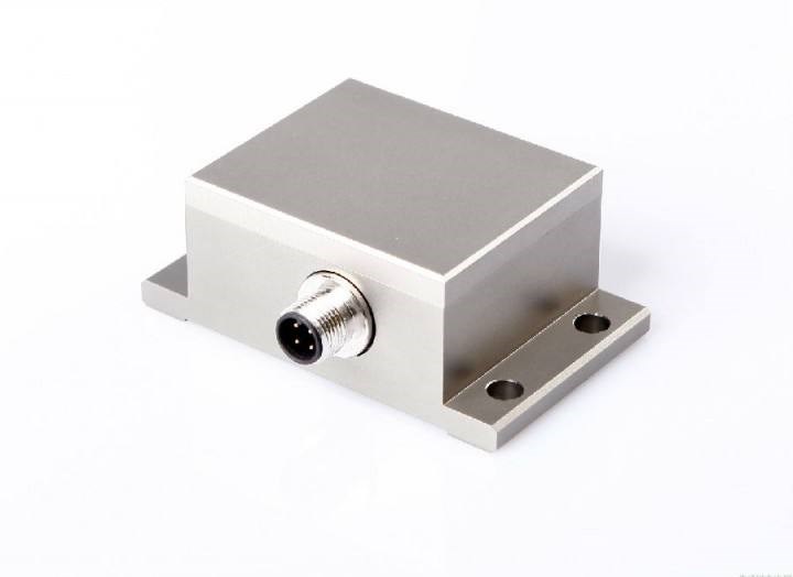
 VB300 3-Axis G-Force Datalogger:Battery Replacement, Features and Application
08 January 20221261
 How to Utilize the TLP250 Isolated MOSFET Driver?
10 March 202221381
 TPS92515QDGQRQ1 LED Drivers: Equivalence, Datasheet, and Pinout
21 March 20221740
 MMBT3906: 250MHz,350mW, Pinout and Datasheet
22 February 20221095
 2N6292 Transistor: Equivalent, Pinout, and Datasheet
29 March 202216704
 ATmega128A 128KB AVR Microcontroller: Datasheet, Pinout, and Design Analysis
13 March 2026310
 TPS92630QPWPRQ1 LED Driver: Pinout, Manufacturer, and Datasheet
23 March 2022344
 Guide to Choosing Ethernet Transceivers for Industrial Networks
09 June 2025246
 What are the Differences in the Copying Methods of Double-Sided and Multi-Layer PCBs?
18 July 20224552
 A Beginner's Guide to the 2N5551 Transistor and Its Uses
27 May 20255653
 Global Semiconductor Market Share Continues to Grow
27 October 20232272
 Thermal Pads vs Thermal Paste Understanding the Key Differences
19 July 20252566
 What are Tilt Sensors?
19 December 20207467
 Comprehensive Introduction to Snapdragon 888
28 June 202115559
 The Evolution History of Storage Devices
26 November 202569462
 Understanding RFID Antennas and Their Role in Modern Technology
30 June 20252862
Texas Instruments
In Stock: 1000
United States
China
Canada
Japan
Russia
Germany
United Kingdom
Singapore
Italy
Hong Kong(China)
Taiwan(China)
France
Korea
Mexico
Netherlands
Malaysia
Austria
Spain
Switzerland
Poland
Thailand
Vietnam
India
United Arab Emirates
Afghanistan
Åland Islands
Albania
Algeria
American Samoa
Andorra
Angola
Anguilla
Antigua & Barbuda
Argentina
Armenia
Aruba
Australia
Azerbaijan
Bahamas
Bahrain
Bangladesh
Barbados
Belarus
Belgium
Belize
Benin
Bermuda
Bhutan
Bolivia
Bonaire, Sint Eustatius and Saba
Bosnia & Herzegovina
Botswana
Brazil
British Indian Ocean Territory
British Virgin Islands
Brunei
Bulgaria
Burkina Faso
Burundi
Cabo Verde
Cambodia
Cameroon
Cayman Islands
Central African Republic
Chad
Chile
Christmas Island
Cocos (Keeling) Islands
Colombia
Comoros
Congo
Congo (DRC)
Cook Islands
Costa Rica
Côte d’Ivoire
Croatia
Cuba
Curaçao
Cyprus
Czechia
Denmark
Djibouti
Dominica
Dominican Republic
Ecuador
Egypt
El Salvador
Equatorial Guinea
Eritrea
Estonia
Eswatini
Ethiopia
Falkland Islands
Faroe Islands
Fiji
Finland
French Guiana
French Polynesia
Gabon
Gambia
Georgia
Ghana
Gibraltar
Greece
Greenland
Grenada
Guadeloupe
Guam
Guatemala
Guernsey
Guinea
Guinea-Bissau
Guyana
Haiti
Honduras
Hungary
Iceland
Indonesia
Iran
Iraq
Ireland
Isle of Man
Israel
Jamaica
Jersey
Jordan
Kazakhstan
Kenya
Kiribati
Kosovo
Kuwait
Kyrgyzstan
Laos
Latvia
Lebanon
Lesotho
Liberia
Libya
Liechtenstein
Lithuania
Luxembourg
Macao(China)
Madagascar
Malawi
Maldives
Mali
Malta
Marshall Islands
Martinique
Mauritania
Mauritius
Mayotte
Micronesia
Moldova
Monaco
Mongolia
Montenegro
Montserrat
Morocco
Mozambique
Myanmar
Namibia
Nauru
Nepal
New Caledonia
New Zealand
Nicaragua
Niger
Nigeria
Niue
Norfolk Island
North Korea
North Macedonia
Northern Mariana Islands
Norway
Oman
Pakistan
Palau
Palestinian Authority
Panama
Papua New Guinea
Paraguay
Peru
Philippines
Pitcairn Islands
Portugal
Puerto Rico
Qatar
Réunion
Romania
Rwanda
Samoa
San Marino
São Tomé & Príncipe
Saudi Arabia
Senegal
Serbia
Seychelles
Sierra Leone
Sint Maarten
Slovakia
Slovenia
Solomon Islands
Somalia
South Africa
South Sudan
Sri Lanka
St Helena, Ascension, Tristan da Cunha
St. Barthélemy
St. Kitts & Nevis
St. Lucia
St. Martin
St. Pierre & Miquelon
St. Vincent & Grenadines
Sudan
Suriname
Svalbard & Jan Mayen
Sweden
Syria
Tajikistan
Tanzania
Timor-Leste
Togo
Tokelau
Tonga
Trinidad & Tobago
Tunisia
Turkey
Turkmenistan
Turks & Caicos Islands
Tuvalu
U.S. Outlying Islands
U.S. Virgin Islands
Uganda
Ukraine
Uruguay
Uzbekistan
Vanuatu
Vatican City
Venezuela
Wallis & Futuna
Yemen
Zambia
Zimbabwe
![SN74ALS139NSR]() SN74ALS139NSR
SN74ALS139NSRTexas Instruments
![SN74CBT3306PWR]() SN74CBT3306PWR
SN74CBT3306PWRTexas Instruments
![SN74CBTS3306PWR]() SN74CBTS3306PWR
SN74CBTS3306PWRTexas Instruments
![SN74LVC157ADBR]() SN74LVC157ADBR
SN74LVC157ADBRTexas Instruments
![SN74LV157APW]() SN74LV157APW
SN74LV157APWTexas Instruments
![SN74CB3Q3306APW]() SN74CB3Q3306APW
SN74CB3Q3306APWTexas Instruments
![SN74HC153N]() SN74HC153N
SN74HC153NTexas Instruments
![SN74AHCT157PW]() SN74AHCT157PW
SN74AHCT157PWTexas Instruments
![SN74CB3T16210DGGR]() SN74CB3T16210DGGR
SN74CB3T16210DGGRTexas Instruments
![SN74CBTLV3245APWR]() SN74CBTLV3245APWR
SN74CBTLV3245APWRTexas Instruments


