
 Product
 Brand
Brand Articles
 Tools
Tools
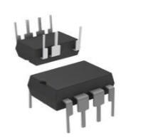
CSD18540Q5B, Pinout, Package

N-Channel Tape & Reel (TR) 2.2m Ω @ 28A, 10V ±20V 4230pF @ 30V 53nC @ 10V 60V 8-PowerTDFN


N-Channel Tape & Reel (TR) 2.2m Ω @ 28A, 10V ±20V 4230pF @ 30V 53nC @ 10V 60V 8-PowerTDFN
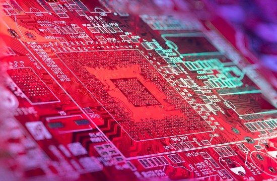
CSD18540Q5B is designed to minimize losses in power conversion applications with a SON 5-mm × 6-mm package. The article is going to introduce the details of the device.
CSD18540Q5B Description
This 1.8-mΩ, 60-V NexFET™ power MOSFET is designed to minimize losses in power conversion applications with a SON 5-mm × 6-mm package.
CSD18540Q5B Pinout

CSD18540Q5B CAD Model
Symbol

Footprint

3D Model

CSD18540Q5B Features
• Ultra-Low Qg and Qgd
• Low-Thermal Resistance
• Avalanche Rated
• Lead-Free Terminal Plating
• RoHS Compliant
• Halogen Free
• SON 5-mm × 6-mm Plastic Package
CSD18540Q5B Recommended PCB Pattern

Specifications
- TypeParameter
- Factory Lead Time6 Weeks
- Mounting Type
The "Mounting Type" in electronic components refers to the method used to attach or connect a component to a circuit board or other substrate, such as through-hole, surface-mount, or panel mount.
Surface Mount - Package / Case
refers to the protective housing that encases an electronic component, providing mechanical support, electrical connections, and thermal management.
8-PowerTDFN - Surface Mount
having leads that are designed to be soldered on the side of a circuit board that the body of the component is mounted on.
YES - Transistor Element Material
The "Transistor Element Material" parameter in electronic components refers to the material used to construct the transistor within the component. Transistors are semiconductor devices that amplify or switch electronic signals and are a fundamental building block in electronic circuits. The material used for the transistor element can significantly impact the performance and characteristics of the component. Common materials used for transistor elements include silicon, germanium, and gallium arsenide, each with its own unique properties and suitability for different applications. The choice of transistor element material is crucial in designing electronic components to meet specific performance requirements such as speed, power efficiency, and temperature tolerance.
SILICON - Current - Continuous Drain (Id) @ 25℃100A Ta
- Drive Voltage (Max Rds On, Min Rds On)4.5V 10V
- Number of Elements1
- Power Dissipation (Max)3.1W Ta 195W Tc
- Operating Temperature
The operating temperature is the range of ambient temperature within which a power supply, or any other electrical equipment, operate in. This ranges from a minimum operating temperature, to a peak or maximum operating temperature, outside which, the power supply may fail.
-55°C~150°C TJ - Packaging
Semiconductor package is a carrier / shell used to contain and cover one or more semiconductor components or integrated circuits. The material of the shell can be metal, plastic, glass or ceramic.
Tape & Reel (TR) - Series
In electronic components, the "Series" refers to a group of products that share similar characteristics, designs, or functionalities, often produced by the same manufacturer. These components within a series typically have common specifications but may vary in terms of voltage, power, or packaging to meet different application needs. The series name helps identify and differentiate between various product lines within a manufacturer's catalog.
NexFET™ - JESD-609 Code
The "JESD-609 Code" in electronic components refers to a standardized marking code that indicates the lead-free solder composition and finish of electronic components for compliance with environmental regulations.
e3 - Pbfree Code
The "Pbfree Code" parameter in electronic components refers to the code or marking used to indicate that the component is lead-free. Lead (Pb) is a toxic substance that has been widely used in electronic components for many years, but due to environmental concerns, there has been a shift towards lead-free alternatives. The Pbfree Code helps manufacturers and users easily identify components that do not contain lead, ensuring compliance with regulations and promoting environmentally friendly practices. It is important to pay attention to the Pbfree Code when selecting electronic components to ensure they meet the necessary requirements for lead-free applications.
yes - Part Status
Parts can have many statuses as they progress through the configuration, analysis, review, and approval stages.
Active - Moisture Sensitivity Level (MSL)
Moisture Sensitivity Level (MSL) is a standardized rating that indicates the susceptibility of electronic components, particularly semiconductors, to moisture-induced damage during storage and the soldering process, defining the allowable exposure time to ambient conditions before they require special handling or baking to prevent failures
1 (Unlimited) - Number of Terminations5
- ECCN Code
An ECCN (Export Control Classification Number) is an alphanumeric code used by the U.S. Bureau of Industry and Security to identify and categorize electronic components and other dual-use items that may require an export license based on their technical characteristics and potential for military use.
EAR99 - Terminal Finish
Terminal Finish refers to the surface treatment applied to the terminals or leads of electronic components to enhance their performance and longevity. It can improve solderability, corrosion resistance, and overall reliability of the connection in electronic assemblies. Common finishes include nickel, gold, and tin, each possessing distinct properties suitable for various applications. The choice of terminal finish can significantly impact the durability and effectiveness of electronic devices.
Matte Tin (Sn) - Additional Feature
Any Feature, including a modified Existing Feature, that is not an Existing Feature.
AVALANCHE RATED - HTS Code
HTS (Harmonized Tariff Schedule) codes are product classification codes between 8-1 digits. The first six digits are an HS code, and the countries of import assign the subsequent digits to provide additional classification. U.S. HTS codes are 1 digits and are administered by the U.S. International Trade Commission.
8541.29.00.95 - Terminal Position
In electronic components, the term "Terminal Position" refers to the physical location of the connection points on the component where external electrical connections can be made. These connection points, known as terminals, are typically used to attach wires, leads, or other components to the main body of the electronic component. The terminal position is important for ensuring proper connectivity and functionality of the component within a circuit. It is often specified in technical datasheets or component specifications to help designers and engineers understand how to properly integrate the component into their circuit designs.
DUAL - Terminal Form
Occurring at or forming the end of a series, succession, or the like; closing; concluding.
NO LEAD - Peak Reflow Temperature (Cel)
Peak Reflow Temperature (Cel) is a parameter that specifies the maximum temperature at which an electronic component can be exposed during the reflow soldering process. Reflow soldering is a common method used to attach electronic components to a circuit board. The Peak Reflow Temperature is crucial because it ensures that the component is not damaged or degraded during the soldering process. Exceeding the specified Peak Reflow Temperature can lead to issues such as component failure, reduced performance, or even permanent damage to the component. It is important for manufacturers and assemblers to adhere to the recommended Peak Reflow Temperature to ensure the reliability and functionality of the electronic components.
260 - Reach Compliance Code
Reach Compliance Code refers to a designation indicating that electronic components meet the requirements set by the Registration, Evaluation, Authorization, and Restriction of Chemicals (REACH) regulation in the European Union. It signifies that the manufacturer has assessed and managed the chemical substances within the components to ensure safety and environmental protection. This code is vital for compliance with regulations aimed at minimizing risks associated with hazardous substances in electronic products.
not_compliant - Time@Peak Reflow Temperature-Max (s)
Time@Peak Reflow Temperature-Max (s) refers to the maximum duration that an electronic component can be exposed to the peak reflow temperature during the soldering process, which is crucial for ensuring reliable solder joint formation without damaging the component.
NOT SPECIFIED - Base Part Number
The "Base Part Number" (BPN) in electronic components serves a similar purpose to the "Base Product Number." It refers to the primary identifier for a component that captures the essential characteristics shared by a group of similar components. The BPN provides a fundamental way to reference a family or series of components without specifying all the variations and specific details.
CSD18540 - JESD-30 Code
JESD-30 Code refers to a standardized descriptive designation system established by JEDEC for semiconductor-device packages. This system provides a systematic method for generating designators that convey essential information about the package's physical characteristics, such as size and shape, which aids in component identification and selection. By using JESD-30 codes, manufacturers and engineers can ensure consistency and clarity in the specification of semiconductor packages across various applications and industries.
R-PDSO-N8 - Configuration
The parameter "Configuration" in electronic components refers to the specific arrangement or setup of the components within a circuit or system. It encompasses how individual elements are interconnected and their physical layout. Configuration can affect the functionality, performance, and efficiency of the electronic system, and may influence factors such as signal flow, impedance, and power distribution. Understanding the configuration is essential for design, troubleshooting, and optimizing electronic devices.
SINGLE WITH BUILT-IN DIODE - Operating Mode
A phase of operation during the operation and maintenance stages of the life cycle of a facility.
ENHANCEMENT MODE - Case Connection
Case Connection refers to the method by which an electronic component's case or housing is connected to the electrical circuit. This connection is important for grounding purposes, mechanical stability, and heat dissipation. The case connection can vary depending on the type of component and its intended application. It is crucial to ensure a secure and reliable case connection to maintain the overall performance and safety of the electronic device.
DRAIN - FET Type
"FET Type" refers to the type of Field-Effect Transistor (FET) being used in an electronic component. FETs are three-terminal semiconductor devices that can be classified into different types based on their construction and operation. The main types of FETs include Metal-Oxide-Semiconductor FETs (MOSFETs), Junction FETs (JFETs), and Insulated-Gate Bipolar Transistors (IGBTs).Each type of FET has its own unique characteristics and applications. MOSFETs are commonly used in digital circuits due to their high input impedance and low power consumption. JFETs are often used in low-noise amplifiers and switching circuits. IGBTs combine the high input impedance of MOSFETs with the high current-carrying capability of bipolar transistors, making them suitable for high-power applications like motor control and power inverters.When selecting an electronic component, understanding the FET type is crucial as it determines the device's performance and suitability for a specific application. It is important to consider factors such as voltage ratings, current handling capabilities, switching speeds, and power dissipation when choosing the right FET type for a particular circuit design.
N-Channel - Transistor Application
In the context of electronic components, the parameter "Transistor Application" refers to the specific purpose or function for which a transistor is designed and used. Transistors are semiconductor devices that can amplify or switch electronic signals and are commonly used in various electronic circuits. The application of a transistor can vary widely depending on its design and characteristics, such as whether it is intended for audio amplification, digital logic, power control, or radio frequency applications. Understanding the transistor application is important for selecting the right type of transistor for a particular circuit or system to ensure optimal performance and functionality.
SWITCHING - Rds On (Max) @ Id, Vgs
Rds On (Max) @ Id, Vgs refers to the maximum on-resistance of a MOSFET or similar transistor when it is fully turned on or in the saturation region. It is specified at a given drain current (Id) and gate-source voltage (Vgs). This parameter indicates how much resistance the component will offer when conducting, impacting power loss and efficiency in a circuit. Lower Rds On values are preferred for better performance in switching applications.
2.2m Ω @ 28A, 10V - Vgs(th) (Max) @ Id
The parameter "Vgs(th) (Max) @ Id" in electronic components refers to the maximum gate-source threshold voltage at a specified drain current (Id). This parameter is commonly found in field-effect transistors (FETs) and is used to define the minimum voltage required at the gate terminal to turn on the transistor and allow current to flow from the drain to the source. The maximum value indicates the upper limit of this threshold voltage under specified operating conditions. It is an important parameter for determining the proper biasing and operating conditions of the FET in a circuit to ensure proper functionality and performance.
2.3V @ 250μA - Input Capacitance (Ciss) (Max) @ Vds
The parameter "Input Capacitance (Ciss) (Max) @ Vds" in electronic components refers to the maximum input capacitance measured at a specific drain-source voltage (Vds). Input capacitance is a crucial parameter in field-effect transistors (FETs) and power MOSFETs, as it represents the total capacitance at the input terminal of the device. This capacitance affects the device's switching speed and overall performance, as it influences the time required for charging and discharging during operation. Manufacturers provide this parameter to help designers understand the device's input characteristics and make informed decisions when integrating it into a circuit.
4230pF @ 30V - Gate Charge (Qg) (Max) @ Vgs
Gate Charge (Qg) (Max) @ Vgs refers to the maximum amount of charge that must be supplied to the gate of a MOSFET or similar device to fully turn it on, measured at a specific gate-source voltage (Vgs). This parameter is crucial for understanding the switching characteristics of the device, as it influences the speed at which the gate can charge and discharge. A higher gate charge value often implies slower switching speeds, which can impact the efficiency of high-frequency applications. This parameter is typically specified in nanocoulombs (nC) in the component's datasheet.
53nC @ 10V - Drain to Source Voltage (Vdss)
The Drain to Source Voltage (Vdss) is a key parameter in electronic components, particularly in field-effect transistors (FETs) such as MOSFETs. It refers to the maximum voltage that can be applied between the drain and source terminals of the FET without causing damage to the component. Exceeding this voltage limit can lead to breakdown and potentially permanent damage to the device.Vdss is an important specification to consider when designing or selecting components for a circuit, as it determines the operating range and reliability of the FET. It is crucial to ensure that the Vdss rating of the component is higher than the maximum voltage expected in the circuit to prevent failures and ensure proper functionality.In summary, the Drain to Source Voltage (Vdss) is a critical parameter that defines the maximum voltage tolerance of a FET component and plays a significant role in determining the overall performance and reliability of electronic circuits.
60V - Vgs (Max)
Vgs (Max) refers to the maximum gate-source voltage that can be applied to a field-effect transistor (FET) without causing damage to the component. This parameter is crucial in determining the safe operating limits of the FET and helps prevent overvoltage conditions that could lead to device failure. Exceeding the specified Vgs (Max) rating can result in breakdown of the gate oxide layer, leading to permanent damage to the FET. Designers must ensure that the applied gate-source voltage does not exceed the maximum rating to ensure reliable and long-term operation of the electronic component.
±20V - Drain Current-Max (Abs) (ID)
The parameter "Drain Current-Max (Abs) (ID)" in electronic components refers to the maximum current that can flow from the drain to the source terminal of a field-effect transistor (FET) or a similar device. It is a crucial specification that indicates the maximum current handling capability of the component before it reaches its saturation point or gets damaged. This parameter is typically specified in amperes (A) and helps designers ensure that the component can safely handle the expected current levels in a circuit without exceeding its limits. It is important to consider this parameter when designing circuits to prevent overloading the component and ensure reliable operation.
28A - Drain-source On Resistance-Max
Drain-source On Resistance-Max, commonly referred to as RDS(on) max, is a specification for MOSFETs that indicates the maximum resistance between the drain and source terminals when the device is turned on. This parameter is critical for assessing the efficiency of a MOSFET in a circuit, as lower values result in reduced power loss and heat generation during operation. It is measured in ohms and is influenced by factors such as temperature and gate-to-source voltage. Understanding RDS(on) max is essential for optimizing performance in power management and switching applications.
0.0033Ohm - Pulsed Drain Current-Max (IDM)
The parameter "Pulsed Drain Current-Max (IDM)" in electronic components refers to the maximum current that the device can handle when operated under pulsed conditions. This specification is important for understanding the device's capability to handle short bursts of high current without causing damage. It is typically measured in amperes and is specified for a specific pulse width and duty cycle. Designers use this parameter to ensure that the component can withstand transient current spikes without failing, making it crucial for applications where pulsed operation is common, such as in power electronics and RF circuits.
400A - DS Breakdown Voltage-Min
The parameter "DS Breakdown Voltage-Min" in electronic components refers to the minimum voltage at which the device will experience a breakdown in its Drain-Source (DS) junction. This voltage represents the point at which the component can no longer effectively regulate or control the flow of current, leading to potential damage or failure. It is an important specification to consider when designing or selecting components for a circuit, as exceeding this breakdown voltage can result in permanent damage to the device. Manufacturers provide this specification to ensure proper usage and to help engineers determine the appropriate operating conditions for the component.
60V - Avalanche Energy Rating (Eas)
Avalanche Energy Rating (Eas) is a parameter that quantifies the energy handling capability of a semiconductor device, particularly during avalanche breakdown conditions. It indicates the maximum energy that the device can withstand without being damaged when it experiences an avalanche effect. This rating is crucial for applications where devices might be exposed to over-voltage or other conditions that could cause unintended breakdown, ensuring reliability and longevity in operation. The Eas value helps designers select appropriate components for circuits that may encounter transient events.
320 mJ - Feedback Cap-Max (Crss)
Feedback Cap-Max (Crss) refers to the maximum capacitance between the output and input of an electronic component, such as a transistor or an operational amplifier. It indicates the level of feedback capacitance that can negatively affect the performance, stability, and bandwidth of the device. A higher Crss value may introduce unintended phase shifts or frequency response issues, making it crucial to consider in circuit design to ensure optimal operation.
20 pF - RoHS Status
RoHS means “Restriction of Certain Hazardous Substances” in the “Hazardous Substances Directive” in electrical and electronic equipment.
ROHS3 Compliant
CSD18540Q5B Applications
• DC-DC Conversion
• Secondary Side Synchronous Rectifier
• Isolated Converter Primary Side Switch
• Motor Control
CSD18540Q5B Package

CSD18540Q5B Manufacturer
Texas Instruments Incorporated (TI) is an American technology company based in Dallas, Texas, that designs and manufactures semiconductors and various integrated circuits, which it sells to electronics designers and manufacturers globally. It is one of the top 10 semiconductor companies worldwide based on sales volume. The company's focus is on developing analog chips and embedded processors, which account for more than 80% of its revenue. TI also produces TI digital light processing technology and education technology products including calculators, micro-controllers, and multi-core processors. The company boasts 45,000 patents around the globe as of 2016.
Trend Analysis
Parts with Similar Specs
What is the recommended operating temperature of the component?
-55°C~150°C TJ.
What is the package of the device?
8-PowerTDFN.
What is the component’s number of pins?
5.
What is designed to minimize power loss?
CSD18540Q5B.
 LM2577 Voltage Regulator: Pinout, Features and Datasheet
29 October 20216212
 IRF640 Power MOSFET: Datasheet, Pinout, and Circuits
28 August 202110943
 ATMEGA328P Microcontroller: Pinout, Datasheet and Application
07 July 202110592
 The Introduction to LM2907
12 August 20218034
![How Can We Use the 2N4403 Transistor? [FAQ]](https://res.utmel.com/Images/Article/b58c969c-7b4d-4cba-a6d1-dd678a3d58f5.jpg) How Can We Use the 2N4403 Transistor? [FAQ]
How Can We Use the 2N4403 Transistor? [FAQ]20 May 20222770
 nRF52810 Multiprotocol SoC : Datasheet, Pinout, Schematic
11 September 20218295
 TNY268PN Switcher: TNY268PN, Datasheet PDF, Application Circuit
21 April 202213621
 Brief introduction of TPS92692QPWPRQ1 LED Controller
22 March 2022541
 Top Batteries That Can Replace LR44
09 June 20251900
 Aluminum Electrolytic Capacitor Basis: Definition, Characteristics and Life
03 March 20225773
 Semiconductor Industry Poised for $1 Trillion Growth Opportunity by 2030
20 November 20233791
 Introduction to USB Type-C
20 February 20232402
 Volkswagen CFO: Chip Supply Shortage Will Continue Until 2024
11 April 20224733
 Trimmer Resistors: From Principles to Selection and Applications
11 August 20251870
 Analyzing the Latest Electronic Components Trends and Their Functions 2023 – 2024
21 July 20252783
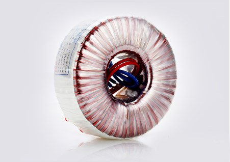 Toroidal transformer: Principles, Features, Types and Applications
13 November 20208744
Texas Instruments
In Stock: 15600
United States
China
Canada
Japan
Russia
Germany
United Kingdom
Singapore
Italy
Hong Kong(China)
Taiwan(China)
France
Korea
Mexico
Netherlands
Malaysia
Austria
Spain
Switzerland
Poland
Thailand
Vietnam
India
United Arab Emirates
Afghanistan
Åland Islands
Albania
Algeria
American Samoa
Andorra
Angola
Anguilla
Antigua & Barbuda
Argentina
Armenia
Aruba
Australia
Azerbaijan
Bahamas
Bahrain
Bangladesh
Barbados
Belarus
Belgium
Belize
Benin
Bermuda
Bhutan
Bolivia
Bonaire, Sint Eustatius and Saba
Bosnia & Herzegovina
Botswana
Brazil
British Indian Ocean Territory
British Virgin Islands
Brunei
Bulgaria
Burkina Faso
Burundi
Cabo Verde
Cambodia
Cameroon
Cayman Islands
Central African Republic
Chad
Chile
Christmas Island
Cocos (Keeling) Islands
Colombia
Comoros
Congo
Congo (DRC)
Cook Islands
Costa Rica
Côte d’Ivoire
Croatia
Cuba
Curaçao
Cyprus
Czechia
Denmark
Djibouti
Dominica
Dominican Republic
Ecuador
Egypt
El Salvador
Equatorial Guinea
Eritrea
Estonia
Eswatini
Ethiopia
Falkland Islands
Faroe Islands
Fiji
Finland
French Guiana
French Polynesia
Gabon
Gambia
Georgia
Ghana
Gibraltar
Greece
Greenland
Grenada
Guadeloupe
Guam
Guatemala
Guernsey
Guinea
Guinea-Bissau
Guyana
Haiti
Honduras
Hungary
Iceland
Indonesia
Iran
Iraq
Ireland
Isle of Man
Israel
Jamaica
Jersey
Jordan
Kazakhstan
Kenya
Kiribati
Kosovo
Kuwait
Kyrgyzstan
Laos
Latvia
Lebanon
Lesotho
Liberia
Libya
Liechtenstein
Lithuania
Luxembourg
Macao(China)
Madagascar
Malawi
Maldives
Mali
Malta
Marshall Islands
Martinique
Mauritania
Mauritius
Mayotte
Micronesia
Moldova
Monaco
Mongolia
Montenegro
Montserrat
Morocco
Mozambique
Myanmar
Namibia
Nauru
Nepal
New Caledonia
New Zealand
Nicaragua
Niger
Nigeria
Niue
Norfolk Island
North Korea
North Macedonia
Northern Mariana Islands
Norway
Oman
Pakistan
Palau
Palestinian Authority
Panama
Papua New Guinea
Paraguay
Peru
Philippines
Pitcairn Islands
Portugal
Puerto Rico
Qatar
Réunion
Romania
Rwanda
Samoa
San Marino
São Tomé & Príncipe
Saudi Arabia
Senegal
Serbia
Seychelles
Sierra Leone
Sint Maarten
Slovakia
Slovenia
Solomon Islands
Somalia
South Africa
South Sudan
Sri Lanka
St Helena, Ascension, Tristan da Cunha
St. Barthélemy
St. Kitts & Nevis
St. Lucia
St. Martin
St. Pierre & Miquelon
St. Vincent & Grenadines
Sudan
Suriname
Svalbard & Jan Mayen
Sweden
Syria
Tajikistan
Tanzania
Timor-Leste
Togo
Tokelau
Tonga
Trinidad & Tobago
Tunisia
Turkey
Turkmenistan
Turks & Caicos Islands
Tuvalu
U.S. Outlying Islands
U.S. Virgin Islands
Uganda
Ukraine
Uruguay
Uzbekistan
Vanuatu
Vatican City
Venezuela
Wallis & Futuna
Yemen
Zambia
Zimbabwe
![CSD25303W1015]() CSD25303W1015
CSD25303W1015Texas Instruments
![CSD18531Q5A]() CSD18531Q5A
CSD18531Q5ATexas Instruments
![CSD25402Q3A]() CSD25402Q3A
CSD25402Q3ATexas Instruments
![CSD18532Q5B]() CSD18532Q5B
CSD18532Q5BTexas Instruments
![CSD16301Q2]() CSD16301Q2
CSD16301Q2Texas Instruments
![CSD17313Q2]() CSD17313Q2
CSD17313Q2Texas Instruments
![CSD18543Q3A]() CSD18543Q3A
CSD18543Q3ATexas Instruments
![CSD16406Q3]() CSD16406Q3
CSD16406Q3Texas Instruments
![CSD18504Q5A]() CSD18504Q5A
CSD18504Q5ATexas Instruments
![CSD19532Q5B]() CSD19532Q5B
CSD19532Q5BTexas Instruments


