
 Product
 Brand
Brand Articles
 Tools
Tools
KSP2222A NPN Transistor: Pinout, Datasheet and Equivalents


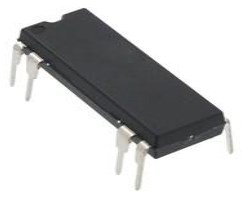
Trans GP BJT NPN 40V 0.6A 3-Pin TO-92 T/R
KSP2222A is an NPN general-purpose amplifier transistor. This post is going to explain pinout, datasheet, equivalent, applications, and more details about the KSP2222A transistor. Furthermore, there is a huge range of semiconductors, capacitors, resistors, and ICs in stock. Welcome your RFQ!

Transistors, how do they work?
- KSP2222A Pinout
- KSP2222A Description
- KSP2222A CAD Model
- Specifications
- KSP2222A Features
- Equivalents for KSP2222A
- Alternatives for KSP2222A
- KSP2222A Applications
- Where to Use KSP2222A
- How to Use KSP2222A
- KSP2222A Physical Dimensions
- KSP2222A Manufacturer
- Parts with Similar Specs
- Popularity by Region
- Datasheet PDF
KSP2222A Pinout

KSP2222A Pinout
| Pin Number | Pin Name | Description |
| 1 | Emitter | Current Drains out through emitter |
| 2 | Base | Controls the biasing of transistor |
| 3 | Collector | Current flows in through collector |
KSP2222A Description
KSP2222A is an NPN transistor hence the collector and emitter will be left open (Reverse biased) when the base pin is held at the ground and will be closed (Forward biased) when a signal is provided to the base pin. The gain value of the KSP2222A is 100 to 300, which controls the transistor's amplification capacity. Because the maximum amount of current that can flow through the Collector pin is 600mA, we can't use this transistor to connect loads that need more than 600mA. We must feed current to the base pin of a transistor to bias it, and this current (IB) should be limited to 5mA.
KSP2222A CAD Model

KSP2222A Footprint

KSP2222A 3D Model
Specifications
- TypeParameter
- Lifecycle Status
Lifecycle Status refers to the current stage of an electronic component in its product life cycle, indicating whether it is active, obsolete, or transitioning between these states. An active status means the component is in production and available for purchase. An obsolete status indicates that the component is no longer being manufactured or supported, and manufacturers typically provide a limited time frame for support. Understanding the lifecycle status is crucial for design engineers to ensure continuity and reliability in their projects.
LAST SHIPMENTS (Last Updated: 1 week ago) - Factory Lead Time6 Weeks
- Mount
In electronic components, the term "Mount" typically refers to the method or process of physically attaching or fixing a component onto a circuit board or other electronic device. This can involve soldering, adhesive bonding, or other techniques to secure the component in place. The mounting process is crucial for ensuring proper electrical connections and mechanical stability within the electronic system. Different components may have specific mounting requirements based on their size, shape, and function, and manufacturers provide guidelines for proper mounting procedures to ensure optimal performance and reliability of the electronic device.
Through Hole - Mounting Type
The "Mounting Type" in electronic components refers to the method used to attach or connect a component to a circuit board or other substrate, such as through-hole, surface-mount, or panel mount.
Through Hole - Package / Case
refers to the protective housing that encases an electronic component, providing mechanical support, electrical connections, and thermal management.
TO-226-3, TO-92-3 (TO-226AA) (Formed Leads) - Number of Pins3
- Weight240mg
- Transistor Element Material
The "Transistor Element Material" parameter in electronic components refers to the material used to construct the transistor within the component. Transistors are semiconductor devices that amplify or switch electronic signals and are a fundamental building block in electronic circuits. The material used for the transistor element can significantly impact the performance and characteristics of the component. Common materials used for transistor elements include silicon, germanium, and gallium arsenide, each with its own unique properties and suitability for different applications. The choice of transistor element material is crucial in designing electronic components to meet specific performance requirements such as speed, power efficiency, and temperature tolerance.
SILICON - Collector-Emitter Breakdown Voltage40V
- Collector-Emitter Saturation Voltage1V
- Number of Elements1
- hFEMin100
- Operating Temperature
The operating temperature is the range of ambient temperature within which a power supply, or any other electrical equipment, operate in. This ranges from a minimum operating temperature, to a peak or maximum operating temperature, outside which, the power supply may fail.
150°C TJ - Packaging
Semiconductor package is a carrier / shell used to contain and cover one or more semiconductor components or integrated circuits. The material of the shell can be metal, plastic, glass or ceramic.
Tape & Reel (TR) - Published2004
- JESD-609 Code
The "JESD-609 Code" in electronic components refers to a standardized marking code that indicates the lead-free solder composition and finish of electronic components for compliance with environmental regulations.
e3 - Pbfree Code
The "Pbfree Code" parameter in electronic components refers to the code or marking used to indicate that the component is lead-free. Lead (Pb) is a toxic substance that has been widely used in electronic components for many years, but due to environmental concerns, there has been a shift towards lead-free alternatives. The Pbfree Code helps manufacturers and users easily identify components that do not contain lead, ensuring compliance with regulations and promoting environmentally friendly practices. It is important to pay attention to the Pbfree Code when selecting electronic components to ensure they meet the necessary requirements for lead-free applications.
yes - Part Status
Parts can have many statuses as they progress through the configuration, analysis, review, and approval stages.
Obsolete - Moisture Sensitivity Level (MSL)
Moisture Sensitivity Level (MSL) is a standardized rating that indicates the susceptibility of electronic components, particularly semiconductors, to moisture-induced damage during storage and the soldering process, defining the allowable exposure time to ambient conditions before they require special handling or baking to prevent failures
1 (Unlimited) - Number of Terminations3
- ECCN Code
An ECCN (Export Control Classification Number) is an alphanumeric code used by the U.S. Bureau of Industry and Security to identify and categorize electronic components and other dual-use items that may require an export license based on their technical characteristics and potential for military use.
EAR99 - Terminal Finish
Terminal Finish refers to the surface treatment applied to the terminals or leads of electronic components to enhance their performance and longevity. It can improve solderability, corrosion resistance, and overall reliability of the connection in electronic assemblies. Common finishes include nickel, gold, and tin, each possessing distinct properties suitable for various applications. The choice of terminal finish can significantly impact the durability and effectiveness of electronic devices.
Tin (Sn) - Voltage - Rated DC
Voltage - Rated DC is a parameter that specifies the maximum direct current (DC) voltage that an electronic component can safely handle without being damaged. This rating is crucial for ensuring the proper functioning and longevity of the component in a circuit. Exceeding the rated DC voltage can lead to overheating, breakdown, or even permanent damage to the component. It is important to carefully consider this parameter when designing or selecting components for a circuit to prevent any potential issues related to voltage overload.
40V - Max Power Dissipation
The maximum power that the MOSFET can dissipate continuously under the specified thermal conditions.
625mW - Terminal Position
In electronic components, the term "Terminal Position" refers to the physical location of the connection points on the component where external electrical connections can be made. These connection points, known as terminals, are typically used to attach wires, leads, or other components to the main body of the electronic component. The terminal position is important for ensuring proper connectivity and functionality of the component within a circuit. It is often specified in technical datasheets or component specifications to help designers and engineers understand how to properly integrate the component into their circuit designs.
BOTTOM - Current Rating
Current rating is the maximum current that a fuse will carry for an indefinite period without too much deterioration of the fuse element.
600mA - Frequency
In electronic components, the parameter "Frequency" refers to the rate at which a signal oscillates or cycles within a given period of time. It is typically measured in Hertz (Hz) and represents how many times a signal completes a full cycle in one second. Frequency is a crucial aspect in electronic components as it determines the behavior and performance of various devices such as oscillators, filters, and communication systems. Understanding the frequency characteristics of components is essential for designing and analyzing electronic circuits to ensure proper functionality and compatibility with other components in a system.
300MHz - Base Part Number
The "Base Part Number" (BPN) in electronic components serves a similar purpose to the "Base Product Number." It refers to the primary identifier for a component that captures the essential characteristics shared by a group of similar components. The BPN provides a fundamental way to reference a family or series of components without specifying all the variations and specific details.
KSP2222 - Element Configuration
The distribution of electrons of an atom or molecule (or other physical structure) in atomic or molecular orbitals.
Single - Power Dissipation
the process by which an electronic or electrical device produces heat (energy loss or waste) as an undesirable derivative of its primary action.
625mW - Gain Bandwidth Product
The gain–bandwidth product (designated as GBWP, GBW, GBP, or GB) for an amplifier is the product of the amplifier's bandwidth and the gain at which the bandwidth is measured.
300MHz - Polarity/Channel Type
In electronic components, the parameter "Polarity/Channel Type" refers to the characteristic that determines the direction of current flow or the type of signal that can be accommodated by the component. For components like diodes and transistors, polarity indicates the direction in which current can flow through the component, such as forward bias or reverse bias for diodes. For components like MOSFETs or JFETs, the channel type refers to whether the component is an N-channel or P-channel device, which determines the type of charge carriers that carry current through the component. Understanding the polarity or channel type of a component is crucial for proper circuit design and ensuring that the component is connected correctly to achieve the desired functionality.
NPN - Transistor Type
Transistor type refers to the classification of transistors based on their operation and construction. The two primary types are bipolar junction transistors (BJTs) and field-effect transistors (FETs). BJTs use current to control the flow of current, while FETs utilize voltage to control current flow. Each type has its own subtypes, such as NPN and PNP for BJTs, and MOSFETs and JFETs for FETs, impacting their applications and characteristics in electronic circuits.
NPN - Collector Emitter Voltage (VCEO)
Collector-Emitter Voltage (VCEO) is a key parameter in electronic components, particularly in transistors. It refers to the maximum voltage that can be applied between the collector and emitter terminals of a transistor while the base terminal is open or not conducting. Exceeding this voltage limit can lead to breakdown and potential damage to the transistor. VCEO is crucial for ensuring the safe and reliable operation of the transistor within its specified limits. Designers must carefully consider VCEO when selecting transistors for a circuit to prevent overvoltage conditions that could compromise the performance and longevity of the component.
40V - Max Collector Current
Max Collector Current is a parameter used to specify the maximum amount of current that can safely flow through the collector terminal of a transistor or other electronic component without causing damage. It is typically expressed in units of amperes (A) and is an important consideration when designing circuits to ensure that the component operates within its safe operating limits. Exceeding the specified max collector current can lead to overheating, degradation of performance, or even permanent damage to the component. Designers must carefully consider this parameter when selecting components and designing circuits to ensure reliable and safe operation.
600mA - DC Current Gain (hFE) (Min) @ Ic, Vce
The parameter "DC Current Gain (hFE) (Min) @ Ic, Vce" in electronic components refers to the minimum value of the DC current gain, denoted as hFE, under specific operating conditions of collector current (Ic) and collector-emitter voltage (Vce). The DC current gain hFE represents the ratio of the collector current to the base current in a bipolar junction transistor (BJT), indicating the amplification capability of the transistor. The minimum hFE value at a given Ic and Vce helps determine the transistor's performance and efficiency in amplifying signals within a circuit. Designers use this parameter to ensure proper transistor selection and performance in various electronic applications.
100 @ 150mA 10mV - Current - Collector Cutoff (Max)
The parameter "Current - Collector Cutoff (Max)" refers to the maximum current at which a transistor or other electronic component will cease to conduct current between the collector and emitter terminals. This parameter is important in determining the maximum current that can flow through the component when it is in the cutoff state. Exceeding this maximum cutoff current can lead to malfunction or damage of the component. It is typically specified in the component's datasheet and is crucial for proper circuit design and operation.
10nA ICBO - Vce Saturation (Max) @ Ib, Ic
The parameter "Vce Saturation (Max) @ Ib, Ic" in electronic components refers to the maximum voltage drop across the collector-emitter junction when the transistor is in saturation mode. This parameter is specified at a certain base current (Ib) and collector current (Ic) levels. It indicates the minimum voltage required to keep the transistor fully conducting in saturation mode, ensuring that the transistor operates efficiently and does not enter the cutoff region. Designers use this parameter to ensure proper transistor operation and to prevent overheating or damage to the component.
1V @ 50mA, 500mA - Transition Frequency
Transition Frequency in electronic components refers to the frequency at which a device can transition from one state to another, typically defining the upper limit of its operating frequency. It is a critical parameter in determining the speed and performance of active components like transistors and integrated circuits. This frequency is influenced by factors such as capacitance, resistance, and the inherent characteristics of the materials used in the component's construction. Understanding transition frequency is essential for optimizing circuit designs and ensuring reliable signal processing in various applications.
300MHz - Max Breakdown Voltage
The "Max Breakdown Voltage" of an electronic component refers to the maximum voltage that the component can withstand across its terminals before it breaks down and allows current to flow uncontrollably. This parameter is crucial in determining the operating limits and safety margins of the component in a circuit. Exceeding the maximum breakdown voltage can lead to permanent damage or failure of the component. It is typically specified by the manufacturer in datasheets to guide engineers and designers in selecting the appropriate components for their applications.
40V - Collector Base Voltage (VCBO)
Collector Base Voltage (VCBO) is the maximum allowable voltage that can be applied between the collector and base terminals of a bipolar junction transistor when the emitter is open. It is a critical parameter that determines the voltage rating of the transistor and helps prevent breakdown in the collector-base junction. Exceeding this voltage can lead to permanent damage or failure of the component.
75V - Emitter Base Voltage (VEBO)
Emitter Base Voltage (VEBO) is a parameter used in electronic components, particularly in transistors. It refers to the maximum voltage that can be applied between the emitter and base terminals of a transistor without causing damage to the device. Exceeding this voltage limit can lead to breakdown of the transistor and potential failure. VEBO is an important specification to consider when designing circuits to ensure the proper operation and reliability of the components. It is typically provided in the datasheet of the transistor and should be carefully observed to prevent any potential damage during operation.
6V - Turn Off Time-Max (toff)
The parameter "Turn Off Time-Max (toff)" in electronic components refers to the maximum time taken for a device to switch from an ON state to an OFF state. It is a crucial specification in devices such as transistors, diodes, and other semiconductor components that control the flow of current. The turn-off time is important for determining the switching speed and efficiency of a component, as a shorter turn-off time generally indicates faster operation and reduced power losses. Designers and engineers use this parameter to ensure proper functioning and performance of electronic circuits and systems.
285ns - Height4.58mm
- Length4.58mm
- Width3.86mm
- Radiation Hardening
Radiation hardening is the process of making electronic components and circuits resistant to damage or malfunction caused by high levels of ionizing radiation, especially for environments in outer space (especially beyond the low Earth orbit), around nuclear reactors and particle accelerators, or during nuclear accidents or nuclear warfare.
No - RoHS Status
RoHS means “Restriction of Certain Hazardous Substances” in the “Hazardous Substances Directive” in electrical and electronic equipment.
RoHS Compliant - Lead Free
Lead Free is a term used to describe electronic components that do not contain lead as part of their composition. Lead is a toxic material that can have harmful effects on human health and the environment, so the electronics industry has been moving towards lead-free components to reduce these risks. Lead-free components are typically made using alternative materials such as silver, copper, and tin. Manufacturers must comply with regulations such as the Restriction of Hazardous Substances (RoHS) directive to ensure that their products are lead-free and environmentally friendly.
Lead Free
KSP2222A Features
Bi-Polar high current NPN Transistor
DC Current Gain (hFE) is 100 to 300
Continuous Collector current (IC) is 600mA
Emitter Base Voltage (VBE) is 6V
Collector-Emitter Voltage (VCE) is 40V
Base Current (IB) is 5mA maximum
Available in To-92 Package
Equivalents for KSP2222A
MPSW01AG, MPS651G, NTE123AP, MPS2222AG, MPSW01A, 2SC1008, BC538, BC547, MPS650, MPS651, MPS650G, P2N2223AG, 2N4401, PN2222A, PN2219A, KN2222A, P2N2222A, KSC1008, MPS2222A, KTN2222A, ZTX450 or PN4033.
KSP2222A Applications
Speed control of Motors
General-purpose NPN transistor
Can be used to switch high current (up to 600mA) loads
It can also be used in various switching applications.
Inverter and other rectifier circuits
Can be used in Darlington Pair
Where to Use KSP2222A
The KSP2222A transistor is very similar to the BC547 NPN transistor, which is widely used. However, there are two key differences between the two. When compared to BC547, KSP2222A can handle collector currents up to 600mA and has a power dissipation of 625mW, allowing it to drive larger loads. A Collector-Emitter open Voltage (VCEo) of 40V is also present.
How to Use KSP2222A
The KSP2222A is an NPN bipolar general-purpose transistor that may be used in a variety of applications and is a direct replacement for the 2N2222A transistor. With the exception of the collector current Ic and the collector-to-emitter voltage VBE, the properties of both NPN transistors are identical.
This transistor is commonly used as an amplifier and switch. Below is a circuit diagram that shows how to utilize the KSP2222A transistor as an amplifier and switch.
KSP2222A as a Switch
The basic and default function of the transistor is to work as a switch. It works in the same way as a mechanical switch, controlling the switch with electrical signals. Consider the following circuit diagram, which shows how to use the KSP2222A NPN transistor to turn on and off a motor or load.

KSP2222A as a Switch
The NPN transistor is driven with a limited base current using the base resistor R1. This reduces the risk of transistor damage. The motor is connected to the R2 resistor, which restricts the amount of current that can pass through the collector terminal.
Only until the voltage across the emitter and base terminals approaches and surpasses the threshold voltage, which is 6 Volts, does the KSP2222A NPN transistor begin to conduct. The type of resistor to employ in the circuit should be determined by the application.
KSP2222A as an Amplifier
Transistors are commonly employed as amplifiers due to their gain (hfe), which is utilized to magnify current or voltage. The following is a circuit diagram for a common emitter (CE) amplifier using the KSP2222A transistor. Despite the fact that there are other amplifier circuits, the CE mode amplifier is often employed to amplify low-frequency voltage signals (for example audio signals).

KSP2222A as an Amplifier
The base and emitter pins of the NPN transistor are linked to the same voltage (supply voltage) in the above circuit, and they are connected to the ground via two resistors R3 and R4. To bias the NPN transistor, the input voltage is delivered to the base terminal. A potential divider network is formed by the resistors R6 and R4. C1 and C2 capacitors are used for filtering.
KSP2222A Physical Dimensions

KSP2222A Physical Dimensions
KSP2222A Manufacturer
On Semiconductor (Nasdaq: ON) is a manufacturer engaging itself in reducing energy use. It features a comprehensive portfolio of power, signal management, and logic, custom solutions that are energy efficient. It acts as a world-class supply chain with high reliability and a network of manufacturing facilities, sales, offices, and design centers in key markets through North America, Europe, and the Asia Pacific regions.
Parts with Similar Specs
- ImagePart NumberManufacturerMountPackage / CaseCollector Emitter Breakdown VoltageMax Collector CurrentTransition FrequencyCollector Emitter Saturation VoltagehFE MinMax Power DissipationView Compare
![KSP2222ATF]()
KSP2222ATF
Through Hole
TO-226-3, TO-92-3 (TO-226AA) (Formed Leads)
40 V
600 mA
300 MHz
1 V
100
625 mW
![PN2222TA]()
Through Hole
TO-226-3, TO-92-3 (TO-226AA) (Formed Leads)
30 V
600 mA
300 MHz
1 V
100
625 mW
![PN2222TF]()
Through Hole
TO-226-3, TO-92-3 (TO-226AA) (Formed Leads)
40 V
600 mA
250 MHz
750 mV
100
625 mW
![2N4401TAR]()
Through Hole
TO-226-3, TO-92-3 (TO-226AA) (Formed Leads)
30 V
600 mA
300 MHz
1 V
100
625 mW

Popularity by Region
Datasheet PDF
- PCN Obsolescence/ EOL :
- PCN Design/Specification :
- Datasheets :
- PCN Packaging :
What can KSP2222A used for?
The applications of the KSP2222A transistor are used as an NPN transistor for general purposes, used to switch high current loads of up to 600 mA and to control the speed of motors.
How does KSP2222A work?
The function of the KSP2222A transistor is similar to the BC547 NPN transistor with a variation in collector current and the power dissipation properties. This transistor allows the continuous collector current IC of the maximum of 600 milli Amps with a power dissipation of 625 mW.
![FDG6335N N-Channel MOSFET: Diagram, Pinout, and Datasheet [Video&FAQ]](https://res.utmel.com/Images/Article/ed8c0389-8d09-46cf-91fb-43c5dd0cf724.png) FDG6335N N-Channel MOSFET: Diagram, Pinout, and Datasheet [Video&FAQ]
FDG6335N N-Channel MOSFET: Diagram, Pinout, and Datasheet [Video&FAQ]28 April 20222849
 STM32H573I-DK Discovery Kit: ARM Cortex-M33 Development Board for IoT
02 July 2025359
 ISO124 Isolation Amplifiers:Pinout, Price and Datasheet PDF
28 June 20216797
.png) 5962-8771602EA: A Versatile Single-Ended Multiplexer for Instrumentation Applications
5962-8771602EA: A Versatile Single-Ended Multiplexer for Instrumentation Applications06 March 2024116
 SI4463 Transceiver: Features, Pinout, and Datasheet
28 October 202112796
 LD39050PU33R: 5.5V, 6-VDFN Exposed Pad, Pinout and Datasheet
02 March 20222015
 HX711 Analog-to-Digital Converter: 24-Bit ADC, HX711 Datasheet, and Load Cell
26 January 202225428
 Step-by-Step NXP MKL03Z32CAF4 Programming Guide
28 May 20251034
 What is Oscilloscope?
24 September 20217968
 A Complete Guide to 2025 Battery vs 2032 Swapping
29 August 20254425
 Pulse Sensor-Definition, Working and Applications
28 January 20214769
 What is LED Drive Power?
18 March 2022790
 Linear Induction Motor: Working Principle, Characteristics, and Applications
02 March 202115520
 Radiation Robustness of Gallium Nitride Power Devices
16 January 20242792
 Solid-state Drive (SSD): Classification and Architecture
22 May 202116945
 What is a MOSFET?
16 April 20217337
ON Semiconductor
In Stock
United States
China
Canada
Japan
Russia
Germany
United Kingdom
Singapore
Italy
Hong Kong(China)
Taiwan(China)
France
Korea
Mexico
Netherlands
Malaysia
Austria
Spain
Switzerland
Poland
Thailand
Vietnam
India
United Arab Emirates
Afghanistan
Åland Islands
Albania
Algeria
American Samoa
Andorra
Angola
Anguilla
Antigua & Barbuda
Argentina
Armenia
Aruba
Australia
Azerbaijan
Bahamas
Bahrain
Bangladesh
Barbados
Belarus
Belgium
Belize
Benin
Bermuda
Bhutan
Bolivia
Bonaire, Sint Eustatius and Saba
Bosnia & Herzegovina
Botswana
Brazil
British Indian Ocean Territory
British Virgin Islands
Brunei
Bulgaria
Burkina Faso
Burundi
Cabo Verde
Cambodia
Cameroon
Cayman Islands
Central African Republic
Chad
Chile
Christmas Island
Cocos (Keeling) Islands
Colombia
Comoros
Congo
Congo (DRC)
Cook Islands
Costa Rica
Côte d’Ivoire
Croatia
Cuba
Curaçao
Cyprus
Czechia
Denmark
Djibouti
Dominica
Dominican Republic
Ecuador
Egypt
El Salvador
Equatorial Guinea
Eritrea
Estonia
Eswatini
Ethiopia
Falkland Islands
Faroe Islands
Fiji
Finland
French Guiana
French Polynesia
Gabon
Gambia
Georgia
Ghana
Gibraltar
Greece
Greenland
Grenada
Guadeloupe
Guam
Guatemala
Guernsey
Guinea
Guinea-Bissau
Guyana
Haiti
Honduras
Hungary
Iceland
Indonesia
Iran
Iraq
Ireland
Isle of Man
Israel
Jamaica
Jersey
Jordan
Kazakhstan
Kenya
Kiribati
Kosovo
Kuwait
Kyrgyzstan
Laos
Latvia
Lebanon
Lesotho
Liberia
Libya
Liechtenstein
Lithuania
Luxembourg
Macao(China)
Madagascar
Malawi
Maldives
Mali
Malta
Marshall Islands
Martinique
Mauritania
Mauritius
Mayotte
Micronesia
Moldova
Monaco
Mongolia
Montenegro
Montserrat
Morocco
Mozambique
Myanmar
Namibia
Nauru
Nepal
New Caledonia
New Zealand
Nicaragua
Niger
Nigeria
Niue
Norfolk Island
North Korea
North Macedonia
Northern Mariana Islands
Norway
Oman
Pakistan
Palau
Palestinian Authority
Panama
Papua New Guinea
Paraguay
Peru
Philippines
Pitcairn Islands
Portugal
Puerto Rico
Qatar
Réunion
Romania
Rwanda
Samoa
San Marino
São Tomé & Príncipe
Saudi Arabia
Senegal
Serbia
Seychelles
Sierra Leone
Sint Maarten
Slovakia
Slovenia
Solomon Islands
Somalia
South Africa
South Sudan
Sri Lanka
St Helena, Ascension, Tristan da Cunha
St. Barthélemy
St. Kitts & Nevis
St. Lucia
St. Martin
St. Pierre & Miquelon
St. Vincent & Grenadines
Sudan
Suriname
Svalbard & Jan Mayen
Sweden
Syria
Tajikistan
Tanzania
Timor-Leste
Togo
Tokelau
Tonga
Trinidad & Tobago
Tunisia
Turkey
Turkmenistan
Turks & Caicos Islands
Tuvalu
U.S. Outlying Islands
U.S. Virgin Islands
Uganda
Ukraine
Uruguay
Uzbekistan
Vanuatu
Vatican City
Venezuela
Wallis & Futuna
Yemen
Zambia
Zimbabwe
![MMBT2222ALT1G]() MMBT2222ALT1G
MMBT2222ALT1GON Semiconductor
![MPSA43]() MPSA43
MPSA43ON Semiconductor
![MMBT3906LT1G]() MMBT3906LT1G
MMBT3906LT1GON Semiconductor
![MMBT5551LT1G]() MMBT5551LT1G
MMBT5551LT1GON Semiconductor
![MMBT4403LT1G]() MMBT4403LT1G
MMBT4403LT1GON Semiconductor
![BC846BLT1G]() BC846BLT1G
BC846BLT1GON Semiconductor
![MMBT3904TT1G]() MMBT3904TT1G
MMBT3904TT1GON Semiconductor
![MMBTA92LT1G]() MMBTA92LT1G
MMBTA92LT1GON Semiconductor
![SMMBT5551LT1G]() SMMBT5551LT1G
SMMBT5551LT1GON Semiconductor
![BCP56-16T1G]() BCP56-16T1G
BCP56-16T1GON Semiconductor


