
 Product
 Brand
Brand Articles
 Tools
Tools
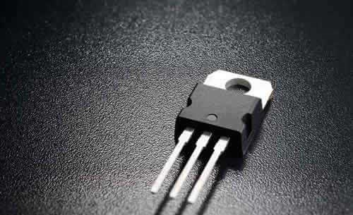
LIS2DW12TR Motion Sensor: Datasheet, Pinout, Application Hint


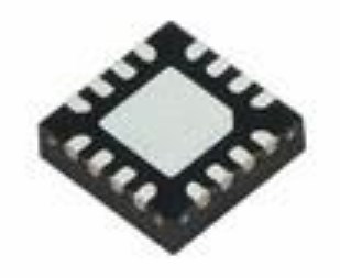
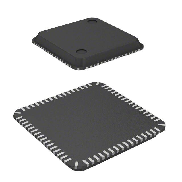
ACCEL 2-16G I2C/SPI 12LGA
The LIS2DW12TR is an ultra-low-power high-performance three-axis linear accelerometer. This article will unlock its datasheet, pinout, application hint, feature and more detailed information about LIS2DW12TR.

Tilt Detection using LIS2DW12
LIS2DW12TR Pinout

LIS2DW12TR Pinout
LIS2DW12TR CAD Model
Symbol

LIS2DW12TR Symbol
Footprint

LIS2DW12TR Footprint
3D Model

LIS2DW12TR 3D Model
LIS2DW12TR Description
The LIS2DW12TR is an ultra-low-power high-performance three-axis linear accelerometer belonging to the “femto” family which leverages the robust and mature manufacturing processes already used for the production of micromachined accelerometers. The LIS2DW12TR has user-selectable full scales of ±2g/±4g/±8g/±16g and is capable of measuring accelerations with output data rates from 1.6 Hz to 1600 Hz.
The LIS2DW12TR has an integrated 32-level first-in, first-out (FIFO) buffer allowing the user to store data in order to limit intervention by the host processor.
The embedded self-test capability allows the user to check the functioning of the sensor in the final application.
The LIS2DW12TR has a dedicated internal engine to process motion and acceleration detection including free-fall, wakeup, highly configurable single/double-tap recognition, activity/inactivity, stationary/motion detection, portrait/landscape detection and 6D/4D orientation.
The LIS2DW12TR is available in a small thin plastic land grid array package (LGA) and it is guaranteed to operate over an extended temperature range from -40°C to +85°C.
LIS2DW12TR Feature
• Ultra-low power consumption: 50 nA in power-down mode, below 1 µA in active low-power mode
• Very low noise: down to 1.3 mg RMS in low-power mode
• Multiple operating modes with multiple bandwidths
• Android stationary detection, motion detection
• Supply voltage, 1.62 V to 3.6 V
• Independent IO supply
• ±2g/±4g/±8g/±16g full scale
• High-speed I²C/SPI digital output interface
• Single data conversion on demand
• 16-bit data output
• Embedded temperature sensor
• Self-test
• 32-level FIFO
• 10000 g high shock survivability
• ECOPACK, RoHS and “Green” compliant
LIS2DW12TR Application
• Motion detection for wearables
• Gesture recognition and gaming
• Motion-activated functions and user interfaces
• Display orientation
• Tap/double-tap recognition
• Free-fall detection
• Smart power saving for handheld devices
• Hearing aids
• Portable healthcare devices
• Wireless sensor nodes
• Motion-enabled metering devices
LIS2DW12TR Block Diagram

LIS2DW12TR Application Hint
The Vdd line provides power to the device core, while the Vdd IO line provides power to the I/O pads. Decoupling capacitors for the power supply (100 nF ceramic, 10 fF aluminium) should be put as close to pin 9 of the device as practicable (common design practice).
To ensure optimal IC behaviour, all voltage and ground supplies must be present at the same time (see the LIS2DW12TR electrical connections (top view) diagram below). Without stopping the communication bus, it is feasible to delete Vdd while keeping Vdd IO; in this case, the measurement chain is turned off.
.jpg")
LIS2DW12 electrical connections (top view)
The device's functionality as well as the measured acceleration data can be selected and accessed via the I2C or SPI interfaces. CS must be tied high (i.e. attached to Vdd IO) while utilizing I2C.
The user can entirely configure the functions, threshold, and timing of the two interrupt pins (INT1 and INT2) using the I2C/SPI interface.
LIS2DW12TR Package

LIS2DW12TR Package
LIS2DW12TR Manufacturer
STMicroelectronics is a global independent semiconductor company and is a leader in developing and delivering semiconductor solutions across the spectrum of microelectronics applications. An unrivalled combination of silicon and system expertise, manufacturing strength, Intellectual Property (IP) portfolio and strategic partners positions the Company at the forefront of System-on-Chip (SoC) technology and its products play a key role in enabling today's convergence trends.
The related articles:
LIS2DH12 Accelerometer: Pinout, Datasheet, and Functional Block Diagram
LIS2DHTR Motion Sensor: 3-Axis, Application Hint, Datasheet PDF
LIS2DE12TR Motion Sensor: Three-Axis Accelerometer, Datasheet, Application Hint and etc.
Specifications
- TypeParameter
- Lifecycle Status
Lifecycle Status refers to the current stage of an electronic component in its product life cycle, indicating whether it is active, obsolete, or transitioning between these states. An active status means the component is in production and available for purchase. An obsolete status indicates that the component is no longer being manufactured or supported, and manufacturers typically provide a limited time frame for support. Understanding the lifecycle status is crucial for design engineers to ensure continuity and reliability in their projects.
ACTIVE (Last Updated: 7 months ago) - Factory Lead Time16 Weeks
- Mounting Type
The "Mounting Type" in electronic components refers to the method used to attach or connect a component to a circuit board or other substrate, such as through-hole, surface-mount, or panel mount.
Surface Mount - Package / Case
refers to the protective housing that encases an electronic component, providing mechanical support, electrical connections, and thermal management.
12-WFLGA - Surface Mount
having leads that are designed to be soldered on the side of a circuit board that the body of the component is mounted on.
YES - Usage LevelIndustrial grade
- Operating Temperature
The operating temperature is the range of ambient temperature within which a power supply, or any other electrical equipment, operate in. This ranges from a minimum operating temperature, to a peak or maximum operating temperature, outside which, the power supply may fail.
-40°C~85°C - Packaging
Semiconductor package is a carrier / shell used to contain and cover one or more semiconductor components or integrated circuits. The material of the shell can be metal, plastic, glass or ceramic.
Tape & Reel (TR) - Part Status
Parts can have many statuses as they progress through the configuration, analysis, review, and approval stages.
Active - Moisture Sensitivity Level (MSL)
Moisture Sensitivity Level (MSL) is a standardized rating that indicates the susceptibility of electronic components, particularly semiconductors, to moisture-induced damage during storage and the soldering process, defining the allowable exposure time to ambient conditions before they require special handling or baking to prevent failures
3 (168 Hours) - Number of Terminations12
- TypeDigital
- Voltage - Supply
Voltage - Supply refers to the range of voltage levels that an electronic component or circuit is designed to operate with. It indicates the minimum and maximum supply voltage that can be applied for the device to function properly. Providing supply voltages outside this range can lead to malfunction, damage, or reduced performance. This parameter is critical for ensuring compatibility between different components in a circuit.
1.62V~3.6V - Terminal Position
In electronic components, the term "Terminal Position" refers to the physical location of the connection points on the component where external electrical connections can be made. These connection points, known as terminals, are typically used to attach wires, leads, or other components to the main body of the electronic component. The terminal position is important for ensuring proper connectivity and functionality of the component within a circuit. It is often specified in technical datasheets or component specifications to help designers and engineers understand how to properly integrate the component into their circuit designs.
BOTTOM - Terminal Form
Occurring at or forming the end of a series, succession, or the like; closing; concluding.
BUTT - Peak Reflow Temperature (Cel)
Peak Reflow Temperature (Cel) is a parameter that specifies the maximum temperature at which an electronic component can be exposed during the reflow soldering process. Reflow soldering is a common method used to attach electronic components to a circuit board. The Peak Reflow Temperature is crucial because it ensures that the component is not damaged or degraded during the soldering process. Exceeding the specified Peak Reflow Temperature can lead to issues such as component failure, reduced performance, or even permanent damage to the component. It is important for manufacturers and assemblers to adhere to the recommended Peak Reflow Temperature to ensure the reliability and functionality of the electronic components.
NOT SPECIFIED - Number of Functions1
- Supply Voltage
Supply voltage refers to the electrical potential difference provided to an electronic component or circuit. It is crucial for the proper operation of devices, as it powers their functions and determines performance characteristics. The supply voltage must be within specified limits to ensure reliability and prevent damage to components. Different electronic devices have specific supply voltage requirements, which can vary widely depending on their design and intended application.
1.8V - Terminal Pitch
The center distance from one pole to the next.
0.5mm - Time@Peak Reflow Temperature-Max (s)
Time@Peak Reflow Temperature-Max (s) refers to the maximum duration that an electronic component can be exposed to the peak reflow temperature during the soldering process, which is crucial for ensuring reliable solder joint formation without damaging the component.
NOT SPECIFIED - Base Part Number
The "Base Part Number" (BPN) in electronic components serves a similar purpose to the "Base Product Number." It refers to the primary identifier for a component that captures the essential characteristics shared by a group of similar components. The BPN provides a fundamental way to reference a family or series of components without specifying all the variations and specific details.
LIS2D - JESD-30 Code
JESD-30 Code refers to a standardized descriptive designation system established by JEDEC for semiconductor-device packages. This system provides a systematic method for generating designators that convey essential information about the package's physical characteristics, such as size and shape, which aids in component identification and selection. By using JESD-30 codes, manufacturers and engineers can ensure consistency and clarity in the specification of semiconductor packages across various applications and industries.
S-XBGA-B12 - Output Type
The "Output Type" parameter in electronic components refers to the type of signal or data that is produced by the component as an output. This parameter specifies the nature of the output signal, such as analog or digital, and can also include details about the voltage levels, current levels, frequency, and other characteristics of the output signal. Understanding the output type of a component is crucial for ensuring compatibility with other components in a circuit or system, as well as for determining how the output signal can be utilized or processed further. In summary, the output type parameter provides essential information about the nature of the signal that is generated by the electronic component as its output.
I2C, SPI - Supply Voltage-Max (Vsup)
The parameter "Supply Voltage-Max (Vsup)" in electronic components refers to the maximum voltage that can be safely applied to the component without causing damage. It is an important specification to consider when designing or using electronic circuits to ensure the component operates within its safe operating limits. Exceeding the maximum supply voltage can lead to overheating, component failure, or even permanent damage. It is crucial to adhere to the specified maximum supply voltage to ensure the reliable and safe operation of the electronic component.
3.6V - Supply Voltage-Min (Vsup)
The parameter "Supply Voltage-Min (Vsup)" in electronic components refers to the minimum voltage level required for the component to operate within its specified performance range. This parameter indicates the lowest voltage that can be safely applied to the component without risking damage or malfunction. It is crucial to ensure that the supply voltage provided to the component meets or exceeds this minimum value to ensure proper functionality and reliability. Failure to adhere to the specified minimum supply voltage may result in erratic behavior, reduced performance, or even permanent damage to the component.
1.62V - Axis
In electronic components, the parameter "Axis" typically refers to the orientation or direction along which a specific characteristic or measurement is being considered. For example, in a sensor or accelerometer, the axis may indicate the direction in which the device is measuring acceleration. In a motor or actuator, the axis may refer to the direction of movement or rotation.Understanding the axis of a component is crucial for proper installation, calibration, and operation. It helps in determining how the component will interact with other parts of a system and how its performance can be optimized. Different components may have multiple axes to consider, especially in complex systems where movement or measurements occur in multiple directions.Overall, the axis parameter provides important information about the spatial orientation or directionality of an electronic component, guiding engineers and technicians in effectively utilizing the component within a larger system.
X, Y, Z - Acceleration Range
The "Acceleration Range" parameter in electronic components refers to the range of acceleration levels that the component can withstand without experiencing damage or malfunction. This parameter is particularly important for components that are used in applications where they may be subjected to varying levels of acceleration, such as in automotive or aerospace systems. The acceleration range is typically specified in units of gravity (g) and indicates the maximum and minimum levels of acceleration that the component can tolerate while still operating within its specified performance limits. It is crucial to consider the acceleration range when selecting components for applications where acceleration levels may vary significantly to ensure reliable and safe operation.
±2g, 4g, 8g, 16g - Features
In the context of electronic components, the term "Features" typically refers to the specific characteristics or functionalities that a particular component offers. These features can vary depending on the type of component and its intended use. For example, a microcontroller may have features such as built-in memory, analog-to-digital converters, and communication interfaces like UART or SPI.When evaluating electronic components, understanding their features is crucial in determining whether they meet the requirements of a particular project or application. Engineers and designers often look at features such as operating voltage, speed, power consumption, and communication protocols to ensure compatibility and optimal performance.In summary, the "Features" parameter in electronic components describes the unique attributes and capabilities that differentiate one component from another, helping users make informed decisions when selecting components for their electronic designs.
Selectable Scale - Sensitivity (LSB/g)
The parameter "Sensitivity (LSB/g)" in electronic components refers to the sensitivity of a sensor or device in terms of the number of least significant bits (LSBs) of output change per unit of acceleration (g). LSB is the smallest change in the digital output of a sensor. This parameter helps to quantify the resolution and accuracy of the sensor in detecting changes in acceleration. A higher sensitivity value indicates that the sensor can detect smaller changes in acceleration, while a lower sensitivity value means that larger changes in acceleration are needed to produce a noticeable output change. It is an important specification to consider when selecting a sensor for applications that require precise measurement of acceleration.
4098 (±2g) ~ 512 (±16g) - Height700μm
- Length2mm
- RoHS Status
RoHS means “Restriction of Certain Hazardous Substances” in the “Hazardous Substances Directive” in electrical and electronic equipment.
Non-RoHS Compliant
Datasheet PDF
- Datasheets :
- Design Resources :
What is LIS2DW12TR?
The ultra-low-power high-performance three-axis linear accelerometer.
What is the output data rate of the LIS2DW12TR?
1.6 Hz to 1600 Hz.
What does the LIS2DW12TR have to process motion and acceleration detection?
A dedicated internal engine.
What is the temperature range of the LIS2DW12TR?
-40°C to +85°C.
 MA700 Angular Sensor: Pinout, Features and Datasheet
21 April 20251016
 TDA7294 DMOS Audio Amplifier: Pinout, Datasheet and Power
18 September 202148041
 STMPS2141STR Microcontroller: 40μA,500mA, Pinout and Features
16 February 20221052
 TPS26600PWPT: High Voltage, Pinout, 4.2V to 55V
18 March 2022758
 MCP23017 I/O Expander: Datasheet, pinout and Addressing
09 September 202112964
 BD136 Transistor: Uses, Price and Datasheet
11 August 20213445
 Understanding the dsPIC33EVXXXGM00X/10X Family of Digital Signal Controller Devices
29 February 2024179
 LTC6990IDCB#TRPBF - Programmable Timer and Oscillator for Precision Timing Applications
06 March 2024249
 How does a Resettable Fuse Work?
26 August 202037191
 Neural Processing Unit (NPU) Explained
15 October 202563064
 What is Power Factor Correction (PFC)?
10 December 20214384
 Introduction to the Types of Monitor Cables
01 April 202416608
 What is a variable capacitor?
16 April 202563208
 What is a Gyroscope Sensor?
11 September 202017912
 What are Varactor Diodes?
24 November 202511719
 What are the Applications of Filters?
17 January 202616840
STMicroelectronics
In Stock: 110880
United States
China
Canada
Japan
Russia
Germany
United Kingdom
Singapore
Italy
Hong Kong(China)
Taiwan(China)
France
Korea
Mexico
Netherlands
Malaysia
Austria
Spain
Switzerland
Poland
Thailand
Vietnam
India
United Arab Emirates
Afghanistan
Åland Islands
Albania
Algeria
American Samoa
Andorra
Angola
Anguilla
Antigua & Barbuda
Argentina
Armenia
Aruba
Australia
Azerbaijan
Bahamas
Bahrain
Bangladesh
Barbados
Belarus
Belgium
Belize
Benin
Bermuda
Bhutan
Bolivia
Bonaire, Sint Eustatius and Saba
Bosnia & Herzegovina
Botswana
Brazil
British Indian Ocean Territory
British Virgin Islands
Brunei
Bulgaria
Burkina Faso
Burundi
Cabo Verde
Cambodia
Cameroon
Cayman Islands
Central African Republic
Chad
Chile
Christmas Island
Cocos (Keeling) Islands
Colombia
Comoros
Congo
Congo (DRC)
Cook Islands
Costa Rica
Côte d’Ivoire
Croatia
Cuba
Curaçao
Cyprus
Czechia
Denmark
Djibouti
Dominica
Dominican Republic
Ecuador
Egypt
El Salvador
Equatorial Guinea
Eritrea
Estonia
Eswatini
Ethiopia
Falkland Islands
Faroe Islands
Fiji
Finland
French Guiana
French Polynesia
Gabon
Gambia
Georgia
Ghana
Gibraltar
Greece
Greenland
Grenada
Guadeloupe
Guam
Guatemala
Guernsey
Guinea
Guinea-Bissau
Guyana
Haiti
Honduras
Hungary
Iceland
Indonesia
Iran
Iraq
Ireland
Isle of Man
Israel
Jamaica
Jersey
Jordan
Kazakhstan
Kenya
Kiribati
Kosovo
Kuwait
Kyrgyzstan
Laos
Latvia
Lebanon
Lesotho
Liberia
Libya
Liechtenstein
Lithuania
Luxembourg
Macao(China)
Madagascar
Malawi
Maldives
Mali
Malta
Marshall Islands
Martinique
Mauritania
Mauritius
Mayotte
Micronesia
Moldova
Monaco
Mongolia
Montenegro
Montserrat
Morocco
Mozambique
Myanmar
Namibia
Nauru
Nepal
New Caledonia
New Zealand
Nicaragua
Niger
Nigeria
Niue
Norfolk Island
North Korea
North Macedonia
Northern Mariana Islands
Norway
Oman
Pakistan
Palau
Palestinian Authority
Panama
Papua New Guinea
Paraguay
Peru
Philippines
Pitcairn Islands
Portugal
Puerto Rico
Qatar
Réunion
Romania
Rwanda
Samoa
San Marino
São Tomé & Príncipe
Saudi Arabia
Senegal
Serbia
Seychelles
Sierra Leone
Sint Maarten
Slovakia
Slovenia
Solomon Islands
Somalia
South Africa
South Sudan
Sri Lanka
St Helena, Ascension, Tristan da Cunha
St. Barthélemy
St. Kitts & Nevis
St. Lucia
St. Martin
St. Pierre & Miquelon
St. Vincent & Grenadines
Sudan
Suriname
Svalbard & Jan Mayen
Sweden
Syria
Tajikistan
Tanzania
Timor-Leste
Togo
Tokelau
Tonga
Trinidad & Tobago
Tunisia
Turkey
Turkmenistan
Turks & Caicos Islands
Tuvalu
U.S. Outlying Islands
U.S. Virgin Islands
Uganda
Ukraine
Uruguay
Uzbekistan
Vanuatu
Vatican City
Venezuela
Wallis & Futuna
Yemen
Zambia
Zimbabwe
![LIS244AL]() LIS244AL
LIS244ALSTMicroelectronics
![AIS2120SXTR]() AIS2120SXTR
AIS2120SXTRSTMicroelectronics
![IIS2DLPCTR]() IIS2DLPCTR
IIS2DLPCTRSTMicroelectronics
![LIS2DH12TR]() LIS2DH12TR
LIS2DH12TRSTMicroelectronics
![LIS3DHTR]() LIS3DHTR
LIS3DHTRSTMicroelectronics
![LIS331DLHTR]() LIS331DLHTR
LIS331DLHTRSTMicroelectronics
![LIS2DE12TR]() LIS2DE12TR
LIS2DE12TRSTMicroelectronics
![LIS344ALHTR]() LIS344ALHTR
LIS344ALHTRSTMicroelectronics
![LIS2DHTR]() LIS2DHTR
LIS2DHTRSTMicroelectronics
![AIS328DQTR]() AIS328DQTR
AIS328DQTRSTMicroelectronics


