
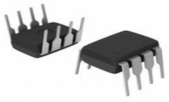
LM2901 Quad Comparator: Pinout, Equivalent and Datasheet


The LM2901 comparator is designed for use in level detection, low−level sensing and memory applications in consumer, automotive, and industrial electronic applications. Furthermore, Huge range of Semiconductors, Capacitors, Resistors and IcS in stock. Welcome RFQ.

Comparator Explained (Inverting Comparator, Non-Inverting Comparator and Window Comparator)
LM2901 Pinout

Pinout
LM2901 CAD Model

Symbol

Footprint

3D Model
LM2901 Overview
The LM2901 comparator is designed for use in level detection, low−level sensing and memory applications in consumer, automotive, and industrial electronic applications. The LM2901 series consists of four independent high-precision voltage comparators with a low offset voltage of 2 for all four comparison mV maximum specifications. These were canceled specifically signed to work in a wide voltage range from a single power supply.
This article provides you with a basic overview of the LM2901 Quad Comparator, including its pin descriptions, features and specifications, etc., to help you quickly understand what LM2901 is.
LM2901 Features
● Single Supply Operation: 3.0 V to 36 V
● Split Supply Operation: ±1.5 V to ±18 V
● Low Input Bias Current: 25 nA (Typ)
● Low Input Offset Current: ±5.0 nA (Typ)
● Low Input Offset Voltage
● Input Common Mode Voltage Range to GND
● Low Output Saturation Voltage: 130 mV (Typ) @ 4.0 mA
● TTL and CMOS Compatible
● ESD Clamps on the Inputs Increase Reliability without Affecting Device Operation
● NCV Prefix for Automotive and Other Applications Requiring Unique Site and Control Change Requirements; AEC−Q100 Qualified and PPAP Capable
● The Device is Pb−Free, Halogen Free/BFR Free and are RoHS Compliant
Specifications
- TypeParameter
LM2901 Functional Block Diagram
.png")
Circuit Schematic (Diagram shown is for 1 comparator)
LM2901 Equivalent
| Model number | Manufacturer | Description |
| LM2901DR2 | On Semiconductor | QUAD COMPARATOR, 15000uV OFFSET-MAX, 1300ns RESPONSE TIME, PDSO14, SOIC-14 |
| LM2901D | Samsung Semiconductor | Comparator, 15000uV Offset-Max, 1400ns Response Time, BIPolar, PDSO14, |
| LM2901M | Fairchild Semiconductor Corporation | Comparator, 4 Func, 15000uV Offset-Max, 1300ns Response Time, BIPolar, PDSO14, SOP-14 |
| LM2901VD | Motorola Semiconductor Products | Comparator, 4 Func, 15000uV Offset-Max, 1300ns Response Time, BIPolar, PDSO14, PLASTIC, SO-14 |
| LM2901VDR2 | On Semiconductor | QUAD COMPARATOR, 15000uV OFFSET-MAX, 1300ns RESPONSE TIME, PDSO14, SOIC-14 |
| KA2901DTF | On Semiconductor | Comparator, Quad, 3000-REEL |
| KA2901DMTF | Rochester Electronics LLC | Comparator, 4 Func, 15000uV Offset-Max, 1400ns Response Time, BIPolar, PDSO14, SOP-14 |
| LM2901QN | Rochester Electronics LLC | Comparator, 4 Func, 15000uV Offset-Max, 1300ns Response Time, BIPolar, PDIP14, PLASTIC, DIP-14 |
| LM2901NG | Rochester Electronics LLC | Comparator, 4 Func, 15000uV Offset-Max, 1300ns Response Time, BIPolar, PDIP14, HALOGEN FREE AND ROHS COMPLIANT PLASTIC DIP-14 |
| LM2901DBLE | Texas Instruments | QUAD COMPARATOR, 15000uV OFFSET-MAX, 1300ns RESPONSE TIME, PDSO14 |
Parts with Similar Specs
LM2901 Applications
● Zero Crossing Detector (Single Supply)
● Zero Crossing Detector (Split Supplies)
● Industrial Electronic Applications
LM2901 Package

Package
LM2901 Marking Diagram

Marking Diagram
LM2901 Soldering Footprint

Soldering Footprint
LM2901 Manufacturer
ON Semiconductor (Nasdaq: ON) is driving energy efficient innovations, empowering customers to reduce global energy use. The company offers a comprehensive portfolio of energy efficient power and signal management, logic, discrete and custom solutions to help design engineers solve their unique design challenges in automotive, communications, computing, consumer, industrial, LED lighting, medical, military/aerospace and power supply applications. ON Semiconductor operates a responsive, reliable, world-class supply chain and quality program, and a network of manufacturing facilities, sales offices and design centers in key markets throughout North America, Europe, and the Asia Pacific regions.
Trend Analysis
What is the difference between LM2901 and LM2904?
LM2901 is a low-power, low-offset voltage quad comparator. LM2904 is a low-power dual operational amplifier.
What is the difference between LM2901DT and LM2901PT?
LM2901DT and LM2901PT are packaged differently. LM2901DT is SO-14 package (small outline package). LM2901PT is in TSSOP-14 package (thin shrinking SOP package).
Since LM2901 cannot be bought, can I directly replace it with LM2902? What is the difference between them?
You cannot directly replace LM2901 with LM2902. Because the pin arrangement of the two is different.
![The Guide to PIC16F1503 8-bit Microcontroller [FAQ]](https://res.utmel.com/Images/Article/ada937dc-8d7f-4372-a00a-b40f9463079c.jpg) The Guide to PIC16F1503 8-bit Microcontroller [FAQ]
The Guide to PIC16F1503 8-bit Microcontroller [FAQ]24 April 20224270
 A Comprehensive Guide to LTC7841EUHE#PBF DC/DC Switching Controller
06 March 202498
 How to Fix Issues with the STM32F091RCT6 Step by Step
24 July 2025254
 MSP430: Detailed Datasheet, Pinout, and Alternatives Guide
22 January 2026135
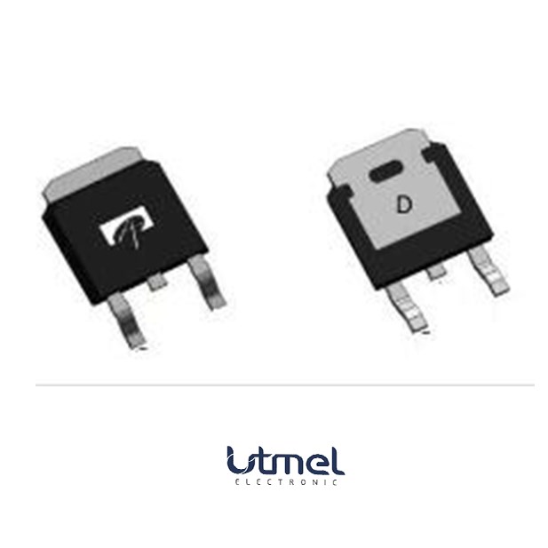 AOD4185:P-Channel Enhancement Mode Field Effect Transistor
09 March 20221270
 LM2904 Dual Op-Amp: Pinout, Features and Application
22 July 20213954
 SI5347 Clock Generator: Features, Pinout and Datasheet
18 April 2022970
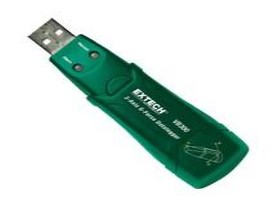 VB300 3-Axis G-Force Datalogger:Battery Replacement, Features and Application
08 January 20221112
 In-Depth Analysis of Q1 2026 Memory Chip Market & Stocking Guide
26 January 20263206
 What is LED Drive Power?
18 March 2022740
 An Overview of Fiber Optic Cable
10 August 20214879
 ON Semiconductor Provides Soft Fourth-Quarter Guidance. The Stock Drops.
13 March 20241247
 What is 3D Printing Technology (3DP)?
18 January 20223668
 Battery Management System (BMS) Implementation Form and Chip Performance Analysis
28 April 20223600
 What are the Types and Dielectric of Ceramic Capacitors?
16 October 202511266
 Introduction To Different Types Of Relays
10 November 202015198
In Stock
United States
China
Canada
Japan
Russia
Germany
United Kingdom
Singapore
Italy
Hong Kong(China)
Taiwan(China)
France
Korea
Mexico
Netherlands
Malaysia
Austria
Spain
Switzerland
Poland
Thailand
Vietnam
India
United Arab Emirates
Afghanistan
Åland Islands
Albania
Algeria
American Samoa
Andorra
Angola
Anguilla
Antigua & Barbuda
Argentina
Armenia
Aruba
Australia
Azerbaijan
Bahamas
Bahrain
Bangladesh
Barbados
Belarus
Belgium
Belize
Benin
Bermuda
Bhutan
Bolivia
Bonaire, Sint Eustatius and Saba
Bosnia & Herzegovina
Botswana
Brazil
British Indian Ocean Territory
British Virgin Islands
Brunei
Bulgaria
Burkina Faso
Burundi
Cabo Verde
Cambodia
Cameroon
Cayman Islands
Central African Republic
Chad
Chile
Christmas Island
Cocos (Keeling) Islands
Colombia
Comoros
Congo
Congo (DRC)
Cook Islands
Costa Rica
Côte d’Ivoire
Croatia
Cuba
Curaçao
Cyprus
Czechia
Denmark
Djibouti
Dominica
Dominican Republic
Ecuador
Egypt
El Salvador
Equatorial Guinea
Eritrea
Estonia
Eswatini
Ethiopia
Falkland Islands
Faroe Islands
Fiji
Finland
French Guiana
French Polynesia
Gabon
Gambia
Georgia
Ghana
Gibraltar
Greece
Greenland
Grenada
Guadeloupe
Guam
Guatemala
Guernsey
Guinea
Guinea-Bissau
Guyana
Haiti
Honduras
Hungary
Iceland
Indonesia
Iran
Iraq
Ireland
Isle of Man
Israel
Jamaica
Jersey
Jordan
Kazakhstan
Kenya
Kiribati
Kosovo
Kuwait
Kyrgyzstan
Laos
Latvia
Lebanon
Lesotho
Liberia
Libya
Liechtenstein
Lithuania
Luxembourg
Macao(China)
Madagascar
Malawi
Maldives
Mali
Malta
Marshall Islands
Martinique
Mauritania
Mauritius
Mayotte
Micronesia
Moldova
Monaco
Mongolia
Montenegro
Montserrat
Morocco
Mozambique
Myanmar
Namibia
Nauru
Nepal
New Caledonia
New Zealand
Nicaragua
Niger
Nigeria
Niue
Norfolk Island
North Korea
North Macedonia
Northern Mariana Islands
Norway
Oman
Pakistan
Palau
Palestinian Authority
Panama
Papua New Guinea
Paraguay
Peru
Philippines
Pitcairn Islands
Portugal
Puerto Rico
Qatar
Réunion
Romania
Rwanda
Samoa
San Marino
São Tomé & Príncipe
Saudi Arabia
Senegal
Serbia
Seychelles
Sierra Leone
Sint Maarten
Slovakia
Slovenia
Solomon Islands
Somalia
South Africa
South Sudan
Sri Lanka
St Helena, Ascension, Tristan da Cunha
St. Barthélemy
St. Kitts & Nevis
St. Lucia
St. Martin
St. Pierre & Miquelon
St. Vincent & Grenadines
Sudan
Suriname
Svalbard & Jan Mayen
Sweden
Syria
Tajikistan
Tanzania
Timor-Leste
Togo
Tokelau
Tonga
Trinidad & Tobago
Tunisia
Turkey
Turkmenistan
Turks & Caicos Islands
Tuvalu
U.S. Outlying Islands
U.S. Virgin Islands
Uganda
Ukraine
Uruguay
Uzbekistan
Vanuatu
Vatican City
Venezuela
Wallis & Futuna
Yemen
Zambia
Zimbabwe