
 Product
 Brand
Brand Articles
 Tools
Tools
LM293 comparators: Schematic, Pinout and Datasheet

Surface Mount Tube 18mA mA 1.3 μs μs Linear Comparators 106.02dB dB 250nA pA 1mA μA 5mV mV Surface Mount
Unit Price: $1.990696
Ext Price: $1.99


Surface Mount Tube 18mA mA 1.3 μs μs Linear Comparators 106.02dB dB 250nA pA 1mA μA 5mV mV Surface Mount
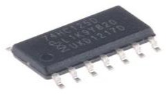
LM293 is a low-power, dual-voltage comparators. This article mainly introduce its schematic, pinout, datasheet and other detailed information about STMicroelectronics LM293.

LM293 Comparator - part 1
LM293 Description
LM293 is a dual independent accurate voltage comparator.
LM293 has a capability to perform its operation from a single supply source as well as from split power supply.
The purpose to design LM293 is to permit a common mode range to the ground level and it perform this operation with single power supply source.
LM293 is the most common device in the market these days due to its high performance and cost effectiveness. This device is considered to be an ideal for a lot of electronics applications.
LM293 has a lot of features which make it different from all other devices. These features include low input offset voltage, low input offset current, low input bias current, wide voltage supply ranges, power supply equal to differential input voltage ranges, lead (Pb) free and lot more.
LM293 can be used at several different places in real life. It can be used in gas sensors, chemical sensors, weigh scales, AC induction, personal computers etc. It is a low cost device and is easily available in the market now a days.
LM293 Pinout

LM293 CAD Model
Symbol

Footprint

3D Model

LM293 Features
●Wide single-supply voltage range or dual supplies: 2 V to 36 V or ±1 V to ±18 V
●Very low supply current (0.45 mA)
●Independent of supply voltage (1 mW/comparator at 5 V)
●Low input bias current: 20 nA typ.
●Low input offset current: ±3 nA typ.
●Low input offset voltage: ±1 mV typ.
●Input common-mode voltage range includes ground
●Low output saturation voltage: 80 mV typ. (Isink = 4 mA)
●Differential input voltage range equal to the supply voltage
●TTL, DTL, ECL, MOS, CMOS compatible outputs
●Available in DFN8 2x2, MiniSO8, TSSOP8, and SO8 packages
●Lead (pb) free
Specifications
- TypeParameter
- Lifecycle Status
Lifecycle Status refers to the current stage of an electronic component in its product life cycle, indicating whether it is active, obsolete, or transitioning between these states. An active status means the component is in production and available for purchase. An obsolete status indicates that the component is no longer being manufactured or supported, and manufacturers typically provide a limited time frame for support. Understanding the lifecycle status is crucial for design engineers to ensure continuity and reliability in their projects.
ACTIVE (Last Updated: 7 months ago) - Factory Lead Time25 Weeks
- Mount
In electronic components, the term "Mount" typically refers to the method or process of physically attaching or fixing a component onto a circuit board or other electronic device. This can involve soldering, adhesive bonding, or other techniques to secure the component in place. The mounting process is crucial for ensuring proper electrical connections and mechanical stability within the electronic system. Different components may have specific mounting requirements based on their size, shape, and function, and manufacturers provide guidelines for proper mounting procedures to ensure optimal performance and reliability of the electronic device.
Surface Mount - Mounting Type
The "Mounting Type" in electronic components refers to the method used to attach or connect a component to a circuit board or other substrate, such as through-hole, surface-mount, or panel mount.
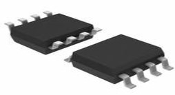
Surface Mount - Package / Case
refers to the protective housing that encases an electronic component, providing mechanical support, electrical connections, and thermal management.
8-SOIC (0.154, 3.90mm Width) - Number of Pins8
- Number of Elements2
- Operating Temperature
The operating temperature is the range of ambient temperature within which a power supply, or any other electrical equipment, operate in. This ranges from a minimum operating temperature, to a peak or maximum operating temperature, outside which, the power supply may fail.
-40°C~105°C - Packaging
Semiconductor package is a carrier / shell used to contain and cover one or more semiconductor components or integrated circuits. The material of the shell can be metal, plastic, glass or ceramic.
Tube - JESD-609 Code
The "JESD-609 Code" in electronic components refers to a standardized marking code that indicates the lead-free solder composition and finish of electronic components for compliance with environmental regulations.
e4 - Part Status
Parts can have many statuses as they progress through the configuration, analysis, review, and approval stages.
Active - Moisture Sensitivity Level (MSL)
Moisture Sensitivity Level (MSL) is a standardized rating that indicates the susceptibility of electronic components, particularly semiconductors, to moisture-induced damage during storage and the soldering process, defining the allowable exposure time to ambient conditions before they require special handling or baking to prevent failures
1 (Unlimited) - Number of Terminations8
- ECCN Code
An ECCN (Export Control Classification Number) is an alphanumeric code used by the U.S. Bureau of Industry and Security to identify and categorize electronic components and other dual-use items that may require an export license based on their technical characteristics and potential for military use.
EAR99 - TypeGeneral Purpose
- Terminal Finish
Terminal Finish refers to the surface treatment applied to the terminals or leads of electronic components to enhance their performance and longevity. It can improve solderability, corrosion resistance, and overall reliability of the connection in electronic assemblies. Common finishes include nickel, gold, and tin, each possessing distinct properties suitable for various applications. The choice of terminal finish can significantly impact the durability and effectiveness of electronic devices.
Nickel/Palladium/Gold (Ni/Pd/Au) - Max Power Dissipation
The maximum power that the MOSFET can dissipate continuously under the specified thermal conditions.
710mW - Terminal Position
In electronic components, the term "Terminal Position" refers to the physical location of the connection points on the component where external electrical connections can be made. These connection points, known as terminals, are typically used to attach wires, leads, or other components to the main body of the electronic component. The terminal position is important for ensuring proper connectivity and functionality of the component within a circuit. It is often specified in technical datasheets or component specifications to help designers and engineers understand how to properly integrate the component into their circuit designs.
DUAL - Terminal Form
Occurring at or forming the end of a series, succession, or the like; closing; concluding.
GULL WING - Peak Reflow Temperature (Cel)
Peak Reflow Temperature (Cel) is a parameter that specifies the maximum temperature at which an electronic component can be exposed during the reflow soldering process. Reflow soldering is a common method used to attach electronic components to a circuit board. The Peak Reflow Temperature is crucial because it ensures that the component is not damaged or degraded during the soldering process. Exceeding the specified Peak Reflow Temperature can lead to issues such as component failure, reduced performance, or even permanent damage to the component. It is important for manufacturers and assemblers to adhere to the recommended Peak Reflow Temperature to ensure the reliability and functionality of the electronic components.
260 - Number of Functions2
- Supply Voltage
Supply voltage refers to the electrical potential difference provided to an electronic component or circuit. It is crucial for the proper operation of devices, as it powers their functions and determines performance characteristics. The supply voltage must be within specified limits to ensure reliability and prevent damage to components. Different electronic devices have specific supply voltage requirements, which can vary widely depending on their design and intended application.
5V - Time@Peak Reflow Temperature-Max (s)
Time@Peak Reflow Temperature-Max (s) refers to the maximum duration that an electronic component can be exposed to the peak reflow temperature during the soldering process, which is crucial for ensuring reliable solder joint formation without damaging the component.
30 - Base Part Number
The "Base Part Number" (BPN) in electronic components serves a similar purpose to the "Base Product Number." It refers to the primary identifier for a component that captures the essential characteristics shared by a group of similar components. The BPN provides a fundamental way to reference a family or series of components without specifying all the variations and specific details.
LM293 - Pin Count
a count of all of the component leads (or pins)
8 - Output Type
The "Output Type" parameter in electronic components refers to the type of signal or data that is produced by the component as an output. This parameter specifies the nature of the output signal, such as analog or digital, and can also include details about the voltage levels, current levels, frequency, and other characteristics of the output signal. Understanding the output type of a component is crucial for ensuring compatibility with other components in a circuit or system, as well as for determining how the output signal can be utilized or processed further. In summary, the output type parameter provides essential information about the nature of the signal that is generated by the electronic component as its output.
CMOS, DTL, ECL, MOS, Open-Collector, TTL - Operating Supply Voltage
The voltage level by which an electrical system is designated and to which certain operating characteristics of the system are related.
28V - Power Supplies
an electronic circuit that converts the voltage of an alternating current (AC) into a direct current (DC) voltage.?
5V - Nominal Supply Current
Nominal current is the same as the rated current. It is the current drawn by the motor while delivering rated mechanical output at its shaft.
1mA - Power Dissipation
the process by which an electronic or electrical device produces heat (energy loss or waste) as an undesirable derivative of its primary action.
710mW - Output Current
The rated output current is the maximum load current that a power supply can provide at a specified ambient temperature. A power supply can never provide more current that it's rated output current unless there is a fault, such as short circuit at the load.
18mA - Max Supply Current
Max Supply Current refers to the maximum amount of electrical current that a component can draw from its power supply under normal operating conditions. It is a critical parameter that ensures the component operates reliably without exceeding its thermal limits or damaging internal circuitry. Exceeding this current can lead to overheating, performance degradation, or failure of the component. Understanding this parameter is essential for designing circuits that provide adequate power while avoiding overload situations.
1mA - Propagation Delay
the flight time of packets over the transmission link and is limited by the speed of light.
1.3 μs - Quiescent Current
The quiescent current is defined as the current level in the amplifier when it is producing an output of zero.
2.5mA - Turn On Delay Time
Turn-on delay, td(on), is the time taken to charge the input capacitance of the device before drain current conduction can start.
1.3 μs - Response Time
the time taken for a circuit or measuring device, when subjected to a change in input signal, to change its state by a specified fraction of its total response to that change.
1.3 μs - Voltage - Supply, Single/Dual (±)
The parameter "Voltage - Supply, Single/Dual (±)" in electronic components refers to the power supply voltage required for the proper operation of the component. This parameter indicates whether the component requires a single power supply voltage (e.g., 5V) or a dual power supply voltage (e.g., ±15V). For components that require a single power supply voltage, only one voltage level is needed for operation. On the other hand, components that require a dual power supply voltage need both positive and negative voltage levels to function correctly.Understanding the voltage supply requirements of electronic components is crucial for designing and integrating them into circuits to ensure proper functionality and prevent damage due to incorrect voltage levels.
2V~36V ±1V~18V - Output Current per Channel
Output Current per Channel is a specification commonly found in electronic components such as amplifiers, audio interfaces, and power supplies. It refers to the maximum amount of electrical current that can be delivered by each individual output channel of the component. This parameter is important because it determines the capacity of the component to drive connected devices or loads. A higher output current per channel means the component can deliver more power to connected devices, while a lower output current may limit the performance or functionality of the component in certain applications. It is crucial to consider the output current per channel when selecting electronic components to ensure they can meet the power requirements of the intended system or setup.
100pA - Input Offset Voltage (Vos)
Input Offset Voltage (Vos) is a key parameter in electronic components, particularly in operational amplifiers. It refers to the voltage difference that must be applied between the two input terminals of the amplifier to nullify the output voltage when the input terminals are shorted together. In simpler terms, it represents the voltage required to bring the output of the amplifier to zero when there is no input signal present. Vos is an important parameter as it can introduce errors in the output signal of the amplifier, especially in precision applications where accuracy is crucial. Minimizing Vos is essential to ensure the amplifier operates with high precision and accuracy.
5mV - Voltage Gain
Voltage gain is a measure of how much an electronic component or circuit amplifies an input voltage signal to produce an output voltage signal. It is typically expressed as a ratio or in decibels (dB). A higher voltage gain indicates a greater amplification of the input signal. Voltage gain is an important parameter in amplifiers, where it determines the level of amplification provided by the circuit. It is calculated by dividing the output voltage by the input voltage and is a key factor in determining the overall performance and functionality of electronic devices.
106.02dB - Average Bias Current-Max (IIB)
The parameter "Average Bias Current-Max (IIB)" in electronic components refers to the maximum average bias current that the component can handle without exceeding its specified operating limits. Bias current is the current that flows through a component when it is in its quiescent state or when it is not actively processing a signal. Exceeding the maximum average bias current can lead to overheating, reduced performance, or even damage to the component. Therefore, it is important to ensure that the bias current does not exceed the specified maximum value to maintain the reliability and longevity of the electronic component.
0.4μA - Supply Voltage Limit-Max
The parameter "Supply Voltage Limit-Max" in electronic components refers to the maximum voltage that the component can safely handle without getting damaged. This specification is crucial for ensuring the reliable operation and longevity of the component within a given electrical system. Exceeding the maximum supply voltage limit can lead to overheating, electrical breakdown, or permanent damage to the component. It is important to carefully adhere to this limit when designing and operating electronic circuits to prevent potential failures and ensure the overall system's performance and safety.
36V - Max Input Current
Max Input Current is a parameter that specifies the maximum amount of electrical current that can safely flow into an electronic component without causing damage. It is an important consideration when designing or using electronic circuits to ensure that the component operates within its specified limits. Exceeding the maximum input current can lead to overheating, component failure, or even pose safety risks. Manufacturers provide this parameter in datasheets to help engineers and users understand the limitations of the component and ensure proper operation within the specified parameters.
250nA - Dual Supply Voltage
Dual Supply Voltage refers to an electronic component's requirement for two separate power supply voltages, typically one positive and one negative. This configuration is commonly used in operational amplifiers, analog circuits, and certain digital devices to allow for greater signal handling capabilities and improved performance. The use of dual supply voltages enables the device to process bipolar signals, thereby enhancing its functionality in various applications.
9V - Input Bias Current
Input Bias Current refers to the small amount of current that flows into the input terminals of an electronic component, such as an operational amplifier. It is primarily caused by the input impedance of the device and the characteristics of the transistors within it. This current is crucial in determining the accuracy of the analog signal processing, as it can affect the level of voltage offset and signal integrity in the application. In many precise applications, minimizing input bias current is essential to achieve optimal performance.
250nA - Voltage - Input Offset (Max)
Voltage - Input Offset (Max) is a parameter that refers to the maximum allowable difference in input voltage between two input terminals of an electronic component, such as an operational amplifier, before the output voltage deviates from the expected value. This parameter is crucial in precision applications where accurate voltage amplification or signal processing is required. A higher value for the input offset voltage indicates a greater potential for error in the output signal, so minimizing this parameter is important for maintaining the accuracy and reliability of the component's performance. Designers often take this parameter into consideration when selecting components for circuits that require precise voltage control and signal processing.
5mV @ 30V - Current - Input Bias (Max)
The parameter "Current - Input Bias (Max)" in electronic components refers to the maximum amount of input bias current that can flow into the input terminal of the component without causing any adverse effects on its performance. Input bias current is the small amount of current that flows into the input terminal of an electronic component, such as an operational amplifier, transistor, or integrated circuit, even when no input signal is applied. This parameter is important because excessive input bias current can lead to errors in the output signal and affect the overall performance of the component. Manufacturers specify a maximum value for input bias current to ensure proper operation and reliability of the component in various applications. It is crucial for designers and engineers to consider this parameter when selecting components for their circuits to ensure optimal performance and functionality.
0.25μA @ 5V - Natural Thermal Resistance
Natural thermal resistance in electronic components refers to the ability of a device to dissipate heat without the assistance of external cooling methods such as fans or liquid cooling. It is a measure of how effectively a component can transfer heat from its junction to its surrounding environment through natural convection and radiation. This parameter is critical for assessing the thermal performance and reliability of electronic devices, as excessive heat can lead to failure or diminished efficiency. Natural thermal resistance is typically expressed in degrees Celsius per watt (°C/W) and is influenced by factors such as the material properties, component design, and ambient conditions.
125 °C/W - Current - Output (Typ)
The parameter "Current - Output (Typ)" in electronic components refers to the typical output current that the component is designed to deliver under normal operating conditions. It represents the expected or average value of the output current that the component can provide. This parameter is important for determining the capability of the component to supply power to other parts of the circuit or system. It helps in ensuring that the component can meet the current requirements of the application without exceeding its specified limits. Manufacturers provide this parameter in datasheets to help designers select the appropriate component for their specific needs.
18mA @ 5V - Height1.58mm
- Length4.9mm
- Width3.9mm
- REACH SVHC
The parameter "REACH SVHC" in electronic components refers to the compliance with the Registration, Evaluation, Authorization, and Restriction of Chemicals (REACH) regulation regarding Substances of Very High Concern (SVHC). SVHCs are substances that may have serious effects on human health or the environment, and their use is regulated under REACH to ensure their safe handling and minimize their impact.Manufacturers of electronic components need to declare if their products contain any SVHCs above a certain threshold concentration and provide information on the safe use of these substances. This information allows customers to make informed decisions about the potential risks associated with using the components and take appropriate measures to mitigate any hazards.Ensuring compliance with REACH SVHC requirements is essential for electronics manufacturers to meet regulatory standards, protect human health and the environment, and maintain transparency in their supply chain. It also demonstrates a commitment to sustainability and responsible manufacturing practices in the electronics industry.
No SVHC - Radiation Hardening
Radiation hardening is the process of making electronic components and circuits resistant to damage or malfunction caused by high levels of ionizing radiation, especially for environments in outer space (especially beyond the low Earth orbit), around nuclear reactors and particle accelerators, or during nuclear accidents or nuclear warfare.
No - RoHS Status
RoHS means “Restriction of Certain Hazardous Substances” in the “Hazardous Substances Directive” in electrical and electronic equipment.
ROHS3 Compliant - Lead Free
Lead Free is a term used to describe electronic components that do not contain lead as part of their composition. Lead is a toxic material that can have harmful effects on human health and the environment, so the electronics industry has been moving towards lead-free components to reduce these risks. Lead-free components are typically made using alternative materials such as silver, copper, and tin. Manufacturers must comply with regulations such as the Restriction of Hazardous Substances (RoHS) directive to ensure that their products are lead-free and environmentally friendly.
Lead Free
LM293 Schematic

LM293 Alternatives

LM293 Applications
★Personal computer
★Chemical sensor
★Gas sensors
★Battery powered systems
★Industrial electronic applications
LM293 Package

Package Outline

Mechanical Data
LM293 Manufacturer
STMicroelectronics is a global independent semiconductor company and is a leader in developing and delivering semiconductor solutions across the spectrum of microelectronics applications. An unrivaled combination of silicon and system expertise, manufacturing strength, Intellectual Property (IP) portfolio and strategic partners positions the Company at the forefront of System-on-Chip (SoC) technology and its products play a key role in enabling today's convergence trends.
Trend Analysis
Datasheet PDF
- Datasheets :
1.What is LM293?
LM193, LM293, and LM393 are comparators with the same function and different grades. Contains two comparators. The prefix 1 is for military products, the prefix 2 is for industrial products, and the prefix 3 is for civilian products.
2.Are LM293 and L293 the same?
Of course it is different. LM293 is a voltage comparator, and L293 is a micro motor drive integrated circuit chip.
3.What is the difference between "LM293" and "LM393"?
There is little difference between LM293 and LM393.
The operating temperature range of LM293 is wider: -25℃~85℃.
The operating temperature range of LM393 is narrower: 0℃~70℃.
Other indicators are the same or have slight differences. In short, LM293 is better than LM393.
4.What is the difference between the chip LM293A and LM293?
The accuracy (input offset voltage) of LM293A is slightly higher than that of LM293.
 STM32F303CBT6 Microcontroller: 32-Bit, 48-LQFP, Pinout and Datasheet
20 January 20223615
 SN74LS32N Positive-OR Gate: Features, Applications and Datasheet
16 October 20233362
 SN74LVC1G17DBVR: Features, Applications, and Datasheet
16 November 20232554
 LM2576 vs LM2596: How to differentiate?
28 April 202218150
 ACS712 Current Sensor: Pinout, Datasheet and Circuit
09 July 202124596
 74HC125 Quad buffer/line driver: Circuit, Pinout and Datasheet
17 August 20213828
 LMG5200 Half-Bridge Power Stage: Feature, Application, and Datasheet
16 June 20214502
 A Comprehensive Overview of the PIC18(L)F2X/4X/5XK42 Microcontroller Family: Architecture, Core Features, and Operation
29 February 2024256
 Enhancing Frequency Stability in Modern Distributed Power Systems
21 September 20244338
 What is a Great Choice for Digital Isolators to Build Isolation Barriers?
31 March 20225232
 Three Phase Inverter - 180 Degree Conduction Mode
05 October 202320840
 TinyML Takes a Major Step Forward as Israeli Company Releases New Chip
19 April 20221134
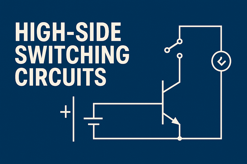 How to Design Reliable High-Side Switching Circuits with P-Channel MOSFETs?
22 July 202512170
 How Proper Thermal Management Extends the Life of Your Electronics
18 July 20251875
 PMIC - Gate Drivers: A Purpose-Built Integrated Circuit
22 February 20234102
 Electronic components in a smart watch
15 May 202310370
STMicroelectronics
In Stock: 100
Minimum: 1 Multiples: 1
Qty
Unit Price
Ext Price
1
$1.990696
$1.99
10
$1.878015
$18.78
100
$1.771712
$177.17
500
$1.671427
$835.71
1000
$1.576818
$1,576.82
Not the price you want? Send RFQ Now and we'll contact you ASAP.
Inquire for More Quantity


