
 Product
 Brand
Brand Articles
 Tools
Tools
MC33164 Micropower Undervoltage Sensing Circuit: Pinout, Features and Datasheet

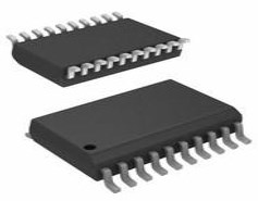
2.4V 8 Terminals 8-Pin MC33164 Voltage supervisor 1 Channels Min 1V Max 10V
Unit Price: $0.530804
Ext Price: $0.53


2.4V 8 Terminals 8-Pin MC33164 Voltage supervisor 1 Channels Min 1V Max 10V
The MC33164 series are undervoltage sensing circuits specifically designed for use as reset controllers in portable microprocessor based systems where extended battery life is required. These devices offer the designer an economical solution for low voltage detection with a single external resistor. Furthermore, Huge range of Semiconductors, Capacitors, Resistors and IcS in stock. Welcome RFQ.
MC33164 Pinout
The following figure is the diagram of MC33164 Pinout.

Pinout
MC33164 CAD Model
The followings are MC33164 Symbol, Footprint, and 3D Model.

PCB Symbol

PCB Footprint

3D Model
MC33164 Overview
The MC33164 series are undervoltage sensing circuits specifically designed for use as reset controllers in portable microprocessor based systems where extended battery life is required. These devices offer the designer an economical solution for low voltage detection with a single external resistor. The MC33164 series features a bandgap reference, a comparator with precise thresholds and built−in hysteresis to prevent erratic reset operation, an open collector reset output capable of sinking in excess of 6.0 mA, and guaranteed operation down to 1.0 V input with extremely low standby current. The MC devices are packaged in 3−pin TO−92 (TO−226AA), micro size TSOP−5, 8−pin SOIC−8 and Micro8™ surface mount packages.
This article provides you with a basic overview of the MC33164 Micropower Undervoltage Sensing Circuit, including its pin descriptions, features and specifications, etc., to help you quickly understand what MC33164 is.
MC33164 Features
● Temperature Compensated Reference
● Precise Comparator Thresholds Guaranteed Over Temperature
● Comparator Hysteresis Prevents Erratic Reset
● Reset Output Capable of Sinking in Excess of 6.0 mA
● Internal Clamp Diode for Discharging Delay Capacitor
● Guaranteed Reset Operation With 1.0 V Input
● Extremely Low Standby Current: As Low as 9.0 μA
● Economical TO−92 (TO−226AA), TSOP−5, SOIC−8 and Micro8 Surface Mount Packages
● NCV Prefix for Automotive and Other Applications Requiring Site and Control Changes
● These Devices are Pb−Free and are RoHS Compliant
Specifications
- TypeParameter
- Lifecycle Status
Lifecycle Status refers to the current stage of an electronic component in its product life cycle, indicating whether it is active, obsolete, or transitioning between these states. An active status means the component is in production and available for purchase. An obsolete status indicates that the component is no longer being manufactured or supported, and manufacturers typically provide a limited time frame for support. Understanding the lifecycle status is crucial for design engineers to ensure continuity and reliability in their projects.
ACTIVE (Last Updated: 2 days ago) - Factory Lead Time4 Weeks
- Mount
In electronic components, the term "Mount" typically refers to the method or process of physically attaching or fixing a component onto a circuit board or other electronic device. This can involve soldering, adhesive bonding, or other techniques to secure the component in place. The mounting process is crucial for ensuring proper electrical connections and mechanical stability within the electronic system. Different components may have specific mounting requirements based on their size, shape, and function, and manufacturers provide guidelines for proper mounting procedures to ensure optimal performance and reliability of the electronic device.
Surface Mount - Mounting Type
The "Mounting Type" in electronic components refers to the method used to attach or connect a component to a circuit board or other substrate, such as through-hole, surface-mount, or panel mount.
Surface Mount - Package / Case
refers to the protective housing that encases an electronic component, providing mechanical support, electrical connections, and thermal management.
8-SOIC (0.154, 3.90mm Width) - Number of Pins8
- Operating Temperature
The operating temperature is the range of ambient temperature within which a power supply, or any other electrical equipment, operate in. This ranges from a minimum operating temperature, to a peak or maximum operating temperature, outside which, the power supply may fail.
-40°C~125°C TA - Packaging
Semiconductor package is a carrier / shell used to contain and cover one or more semiconductor components or integrated circuits. The material of the shell can be metal, plastic, glass or ceramic.
Tube - Published1997
- JESD-609 Code
The "JESD-609 Code" in electronic components refers to a standardized marking code that indicates the lead-free solder composition and finish of electronic components for compliance with environmental regulations.
e3 - Pbfree Code
The "Pbfree Code" parameter in electronic components refers to the code or marking used to indicate that the component is lead-free. Lead (Pb) is a toxic substance that has been widely used in electronic components for many years, but due to environmental concerns, there has been a shift towards lead-free alternatives. The Pbfree Code helps manufacturers and users easily identify components that do not contain lead, ensuring compliance with regulations and promoting environmentally friendly practices. It is important to pay attention to the Pbfree Code when selecting electronic components to ensure they meet the necessary requirements for lead-free applications.
yes - Part Status
Parts can have many statuses as they progress through the configuration, analysis, review, and approval stages.
Active - Moisture Sensitivity Level (MSL)
Moisture Sensitivity Level (MSL) is a standardized rating that indicates the susceptibility of electronic components, particularly semiconductors, to moisture-induced damage during storage and the soldering process, defining the allowable exposure time to ambient conditions before they require special handling or baking to prevent failures
1 (Unlimited) - Number of Terminations8
- ECCN Code
An ECCN (Export Control Classification Number) is an alphanumeric code used by the U.S. Bureau of Industry and Security to identify and categorize electronic components and other dual-use items that may require an export license based on their technical characteristics and potential for military use.
EAR99 - TypeSimple Reset/Power-On Reset
- Terminal Finish
Terminal Finish refers to the surface treatment applied to the terminals or leads of electronic components to enhance their performance and longevity. It can improve solderability, corrosion resistance, and overall reliability of the connection in electronic assemblies. Common finishes include nickel, gold, and tin, each possessing distinct properties suitable for various applications. The choice of terminal finish can significantly impact the durability and effectiveness of electronic devices.
Tin (Sn) - Max Power Dissipation
The maximum power that the MOSFET can dissipate continuously under the specified thermal conditions.
700mW - Terminal Position
In electronic components, the term "Terminal Position" refers to the physical location of the connection points on the component where external electrical connections can be made. These connection points, known as terminals, are typically used to attach wires, leads, or other components to the main body of the electronic component. The terminal position is important for ensuring proper connectivity and functionality of the component within a circuit. It is often specified in technical datasheets or component specifications to help designers and engineers understand how to properly integrate the component into their circuit designs.
DUAL - Terminal Form
Occurring at or forming the end of a series, succession, or the like; closing; concluding.
GULL WING - Peak Reflow Temperature (Cel)
Peak Reflow Temperature (Cel) is a parameter that specifies the maximum temperature at which an electronic component can be exposed during the reflow soldering process. Reflow soldering is a common method used to attach electronic components to a circuit board. The Peak Reflow Temperature is crucial because it ensures that the component is not damaged or degraded during the soldering process. Exceeding the specified Peak Reflow Temperature can lead to issues such as component failure, reduced performance, or even permanent damage to the component. It is important for manufacturers and assemblers to adhere to the recommended Peak Reflow Temperature to ensure the reliability and functionality of the electronic components.
260 - Number of Functions1
- Supply Voltage
Supply voltage refers to the electrical potential difference provided to an electronic component or circuit. It is crucial for the proper operation of devices, as it powers their functions and determines performance characteristics. The supply voltage must be within specified limits to ensure reliability and prevent damage to components. Different electronic devices have specific supply voltage requirements, which can vary widely depending on their design and intended application.
2.4V - Time@Peak Reflow Temperature-Max (s)
Time@Peak Reflow Temperature-Max (s) refers to the maximum duration that an electronic component can be exposed to the peak reflow temperature during the soldering process, which is crucial for ensuring reliable solder joint formation without damaging the component.
40 - Base Part Number
The "Base Part Number" (BPN) in electronic components serves a similar purpose to the "Base Product Number." It refers to the primary identifier for a component that captures the essential characteristics shared by a group of similar components. The BPN provides a fundamental way to reference a family or series of components without specifying all the variations and specific details.
MC33164 - Output
In electronic components, the parameter "Output" typically refers to the signal or data that is produced by the component and sent to another part of the circuit or system. The output can be in the form of voltage, current, frequency, or any other measurable quantity depending on the specific component. The output of a component is often crucial in determining its functionality and how it interacts with other components in the circuit. Understanding the output characteristics of electronic components is essential for designing and troubleshooting electronic circuits effectively.
Open Drain or Open Collector - Pin Count
a count of all of the component leads (or pins)
8 - Output Voltage
Output voltage is a crucial parameter in electronic components that refers to the voltage level produced by the component as a result of its operation. It represents the electrical potential difference between the output terminal of the component and a reference point, typically ground. The output voltage is a key factor in determining the performance and functionality of the component, as it dictates the level of voltage that will be delivered to the connected circuit or load. It is often specified in datasheets and technical specifications to ensure compatibility and proper functioning within a given system.
4.45V - Power Supplies
an electronic circuit that converts the voltage of an alternating current (AC) into a direct current (DC) voltage.?
5V - Number of Channels1
- Max Supply Voltage
In general, the absolute maximum common-mode voltage is VEE-0.3V and VCC+0.3V, but for products without a protection element at the VCC side, voltages up to the absolute maximum rated supply voltage (i.e. VEE+36V) can be supplied, regardless of supply voltage.
10V - Min Supply Voltage
The minimum supply voltage (V min ) is explored for sequential logic circuits by statistically simulating the impact of within-die process variations and gate-dielectric soft breakdown on data retention and hold time.
1V - Operating Supply Current
Operating Supply Current, also known as supply current or quiescent current, is a crucial parameter in electronic components that indicates the amount of current required for the device to operate under normal conditions. It represents the current drawn by the component from the power supply while it is functioning. This parameter is important for determining the power consumption of the component and is typically specified in datasheets to help designers calculate the overall power requirements of their circuits. Understanding the operating supply current is essential for ensuring proper functionality and efficiency of electronic systems.
32μA - Power Dissipation
the process by which an electronic or electrical device produces heat (energy loss or waste) as an undesirable derivative of its primary action.
700mW - Adjustable Threshold
The "Adjustable Threshold" parameter in electronic components refers to the ability to manually set or modify the threshold level at which a specific function or operation is triggered. This feature allows users to customize the sensitivity or activation point of the component according to their specific requirements or preferences. By adjusting the threshold, users can fine-tune the performance of the component to suit different applications or environmental conditions. This flexibility in threshold adjustment can be particularly useful in various electronic devices and systems where precise control over triggering levels is necessary for optimal functionality.
NO - Reset
The "Reset" parameter in electronic components refers to a function that initializes or sets a device to a predefined state. It is often used to clear any temporary data, errors, or configurations that may have been stored during operation. The reset process can ensure that the device starts from a known good state, allowing for reliable performance in subsequent tasks. This parameter is critical in digital circuits and systems where proper initialization is necessary for correct functioning.
Active Low - Number of Voltages Monitored
Voltage monitoring relays can detect not only under-voltages and over-voltages, but also voltage-related issues such as phase imbalances, phase loss, and phase sequence. Voltage monitoring relays are designed for either single-phase or three-phase systems.
1 - Halogen Free
The term "Halogen Free" in electronic components refers to a specific characteristic of the materials used in the manufacturing of the component. Halogens are a group of elements that include fluorine, chlorine, bromine, iodine, and astatine. These elements are commonly used in flame retardants and other materials in electronics. However, the presence of halogens can pose environmental and health risks when the components are disposed of or recycled.Therefore, electronic components labeled as "Halogen Free" are manufactured without the use of halogenated materials. This designation indicates that the components do not contain any halogens, making them safer for the environment and human health. Halogen-free components are becoming increasingly popular in the electronics industry due to the growing awareness of environmental concerns and regulations regarding hazardous substances in electronic products.
Halogen Free - Supply Current-Max (Isup)
Supply Current-Max (Isup) refers to the maximum amount of current that an electronic component can draw from its power supply during operation. It represents the peak current demand of the device under normal operating conditions and is critical for ensuring that the power supply can adequately support the component's needs without risking damage or malfunction. This parameter is essential for designing circuits and selecting appropriate power supply units to prevent overloading and ensure reliable performance.
0.05mA - Min Reset Threshold Voltage
Min Reset Threshold Voltage refers to the minimum voltage level at which a device, such as a microcontroller or a voltage supervisor, can reliably reset its internal state. When the supply voltage drops below this threshold, the device initiates a reset process to clear the current execution state and restore it to a known initial condition. This parameter is critical for ensuring proper operation during power fluctuations, preventing unintended behavior from occurring due to insufficient voltage.
4.15V - Max Reset Threshold Voltage
Max Reset Threshold Voltage refers to the maximum voltage level at which an electronic component, such as a voltage regulator or a reset circuit, will reset or initialize itself. When the input voltage exceeds this threshold, the component typically enters a defined state, often resetting its output or operational mode. It is a critical specification to ensure reliable operation and prevent unexpected behavior in electronic devices. This parameter is important for design considerations in applications where voltage fluctuations or spikes may occur.
4.45V - Threshold Voltage
The threshold voltage is a critical parameter in electronic components, particularly in field-effect transistors (FETs). It refers to the minimum voltage required at the input terminal of the FET to turn it on and allow current to flow between the source and drain terminals. Below the threshold voltage, the FET remains in the off state, acting as an open switch. Once the threshold voltage is exceeded, the FET enters the on state, conducting current between the source and drain.The threshold voltage is a key factor in determining the operating characteristics of FETs, such as their switching speed and power consumption. It is typically specified by the manufacturer and can vary depending on the specific type of FET and its design. Designers must consider the threshold voltage when selecting FETs for a particular application to ensure proper functionality and performance.
+4.33V - Undervoltage Threshold
During power up and power down, the UVLO function of the device has at least 0.1 V of hysteresis, but not more than 0.3 V. The UVLO function in power devices is a useful feature that enables robust system behavior across a wide range of operating conditions.
4.33V - Overvoltage Threshold
Overvoltages are all voltages that temporarily surpass the threshold value of the mains voltage. However, overvoltages can not only occur in the 230 V (normal household power supply voltage) mains, but can also reach the connected devices via telephone or aerial cables.
4.45V - Height1.5mm
- Length5mm
- Width4mm
- REACH SVHC
The parameter "REACH SVHC" in electronic components refers to the compliance with the Registration, Evaluation, Authorization, and Restriction of Chemicals (REACH) regulation regarding Substances of Very High Concern (SVHC). SVHCs are substances that may have serious effects on human health or the environment, and their use is regulated under REACH to ensure their safe handling and minimize their impact.Manufacturers of electronic components need to declare if their products contain any SVHCs above a certain threshold concentration and provide information on the safe use of these substances. This information allows customers to make informed decisions about the potential risks associated with using the components and take appropriate measures to mitigate any hazards.Ensuring compliance with REACH SVHC requirements is essential for electronics manufacturers to meet regulatory standards, protect human health and the environment, and maintain transparency in their supply chain. It also demonstrates a commitment to sustainability and responsible manufacturing practices in the electronics industry.
No SVHC - Radiation Hardening
Radiation hardening is the process of making electronic components and circuits resistant to damage or malfunction caused by high levels of ionizing radiation, especially for environments in outer space (especially beyond the low Earth orbit), around nuclear reactors and particle accelerators, or during nuclear accidents or nuclear warfare.
No - RoHS Status
RoHS means “Restriction of Certain Hazardous Substances” in the “Hazardous Substances Directive” in electrical and electronic equipment.
ROHS3 Compliant - Lead Free
Lead Free is a term used to describe electronic components that do not contain lead as part of their composition. Lead is a toxic material that can have harmful effects on human health and the environment, so the electronics industry has been moving towards lead-free components to reduce these risks. Lead-free components are typically made using alternative materials such as silver, copper, and tin. Manufacturers must comply with regulations such as the Restriction of Hazardous Substances (RoHS) directive to ensure that their products are lead-free and environmentally friendly.
Lead Free
MC33164 Functional Block Diagram
The following is the Block Diagram of MC33164.

Representative Block Diagram
MC33164 Equivalent
| Model number | Manufacturer | Description |
| MC33164D-5 | Motorola Mobility LLC | 1-CHANNEL POWER SUPPLY SUPPORT CKT, PDSO8, PLASTIC, SOIC-8 |
| MC33164D-5R2 | Motorola Semiconductor Products | Power Supply Support Circuit, Fixed, 1 Channel, PDSO8, PLASTIC, SOIC-8 |
Parts with Similar Specs
- ImagePart NumberManufacturerPackage / CaseNumber of PinsNumber of Voltages MonitoredResetOvervoltage ThresholdUndervoltage ThresholdThreshold VoltageMin Supply VoltageSupply VoltageView Compare
![MC33164D-5G]()
MC33164D-5G
8-SOIC (0.154, 3.90mm Width)
8
1
Active Low
4.45 V
4.33 V
+4.33V
1 V
2.4 V
![MC34164D-5R2G]()
8-SOIC (0.154, 3.90mm Width)
8
1
Active Low
4.45 V
4.33 V
+4.33V
1 V
2.4 V
![MC34164D-5G]()
8-SOIC (0.154, 3.90mm Width)
8
1
Active Low
4.45 V
4.33 V
+4.33V
1 V
2.4 V
![MC34164D-005]()
8-SOIC (0.154, 3.90mm Width)
8
1
Active Low
4.45 V
4.33 V
+4.33V
1 V
5 V
![MCP130-475I/SN]()
8-SOIC (0.154, 3.90mm Width)
8
1
Active Low
4.75 V
4.5 V
+4.63V
1 V
5 V


MC33164 Applications
Applications include direct monitoring of the 3.0 V or 5.0 V MPU/logic power supply used in appliance, automotive, consumer, and industrial equipment.
MC33164 Package
The following diagrams show the MC33164 Package.

View A

View B

View C
MC33164 Package Soldering Footprint
The following diagram shows the MC33164 Package Soldering Footprint.

Soldering Footprint
MC33164 Marking Diagram
The following is the Marking Diagram of MC33164.

Marking Diagram
MC33164 Manufacturer
ON Semiconductor (Nasdaq: ON) is driving energy efficient innovations, empowering customers to reduce global energy use. The company offers a comprehensive portfolio of energy efficient power and signal management, logic, discrete and custom solutions to help design engineers solve their unique design challenges in automotive, communications, computing, consumer, industrial, LED lighting, medical, military/aerospace and power supply applications. ON Semiconductor operates a responsive, reliable, world-class supply chain and quality program, and a network of manufacturing facilities, sales offices and design centers in key markets throughout North America, Europe, and the Asia Pacific regions.
Datasheet PDF
- Datasheets :
- Environmental Information :
How many pins of MC33164D-5G?
8 Pins.
What’s the operating temperature of MC33164D-5G?
-40°C~125°C TA.
What is the essential property of the MC33164?
The MC33164 series are undervoltage sensing circuits specifically designed for use as reset controllers in portable microprocessor based systems where extended battery life is required.
 Battery CR2430: 3V Lithium Battery, CR2430 Equivalents and CR2430 VS CR2032
06 December 202155510
![LM2940 voltage regulator[video+FAQ]: Datasheet, circuit and Equivalent](https://res.utmel.com/Images/Article/aee84180-9b54-409c-9d10-37b8b033fb48.jpg) LM2940 voltage regulator[video+FAQ]: Datasheet, circuit and Equivalent
LM2940 voltage regulator[video+FAQ]: Datasheet, circuit and Equivalent28 April 20227412
 LD1117V33 Regulator: Pinout, Applications and Datasheet
18 October 20232052
 MCP2200 Converter: Features, Pinout, and Datasheet
24 November 20212091
 CP2102 Bridge Driver: Alternative, Pinout and Datasheet
14 July 20218661
 TPS54824RNVR: 18-VFQFN, Step-Down, Pinout, Datasheet
26 February 20221242
 74HC125 Quad buffer/line driver: Circuit, Pinout and Datasheet
17 August 20213203
![PC817 Optoisolators Transistor Photovoltaic 4DIP[Video]: Pinout, Datasheet, and Equivalents](https://res.utmel.com/Images/Article/c21d5d4a-7f97-47d9-a2df-3305ccf27127.jpg) PC817 Optoisolators Transistor Photovoltaic 4DIP[Video]: Pinout, Datasheet, and Equivalents
PC817 Optoisolators Transistor Photovoltaic 4DIP[Video]: Pinout, Datasheet, and Equivalents24 March 20223995
 Amorphous Silicon Solar Cells: Features, Structure and Applications
22 August 20225580
 What are Laser Diodes?
20 October 202514642
 Hybrid Sources Powered Electric Vehicles - Part 2
20 March 20232844
 Toggle Switches: Features, Types and Applications
23 January 202110636
 Trends in the Semiconductor Industry in 2022
14 February 20222591
 What is Power over Ethernet(PoE)?
01 December 20212682
 RF Switches Guide: Types, Specifications & Applications
03 July 20253419
 Building a Smart Home System: Exploring Arduino Applications
13 March 20242520
ON Semiconductor
In Stock
Minimum: 1 Multiples: 1
Qty
Unit Price
Ext Price
1
$0.530804
$0.53
10
$0.500759
$5.01
100
$0.472414
$47.24
500
$0.445674
$222.84
1000
$0.420447
$420.45
Not the price you want? Send RFQ Now and we'll contact you ASAP.
Inquire for More Quantity
![CAT809JTBI-GT3]() CAT809JTBI-GT3
CAT809JTBI-GT3ON Semiconductor
![MAX809LTRG]() MAX809LTRG
MAX809LTRGON Semiconductor
![CAT809STBI-GT3]() CAT809STBI-GT3
CAT809STBI-GT3ON Semiconductor
![MC33161DMR2G]() MC33161DMR2G
MC33161DMR2GON Semiconductor
![MC33164D-5R2G]() MC33164D-5R2G
MC33164D-5R2GON Semiconductor
![MC33161DG]() MC33161DG
MC33161DGON Semiconductor
![MC34161DR2G]() MC34161DR2G
MC34161DR2GON Semiconductor
![NCP303LSN10T1G]() NCP303LSN10T1G
NCP303LSN10T1GON Semiconductor
![MC33161DR2G]() MC33161DR2G
MC33161DR2GON Semiconductor
![NCP303LSN09T1G]() NCP303LSN09T1G
NCP303LSN09T1GON Semiconductor


