

 Product
 Brand
Brand Articles
 Tools
Tools
OPA2134PA Audio Amplifier:Circuit, Pinout and Equivalent[FAQ+Video]

35mA per Channel 5pA 86 dB Instrumentational OP Amps 0.0001μA 5V~36V ±2.5V~18V OPA2134 8 Pins 8-DIP (0.300, 7.62mm)
Unit Price: $4.854966
Ext Price: $4.85


35mA per Channel 5pA 86 dB Instrumentational OP Amps 0.0001μA 5V~36V ±2.5V~18V OPA2134 8 Pins 8-DIP (0.300, 7.62mm)
The OPA134 series are ultra-low distortion, low-noise operational amplifiers fully specified for audio applications. This article will introduce OPA2134PA for you from the perspectives of equivalent, datasheet, circuit, pinout, and other relatives.

More Re branded OPA2134PA Op Amps Exposed!!!
- OPA2134PA Description
- OPA2134PA CAD Models
- OPA2134PA Pinout and Configurations
- Specifications
- OPA2134PA Features
- OPA2134P Applications
- OPA2134PA Functional Block Diagram
- OPA2134PA Dimensions
- OPA2134PA Substitutes
- OPA2134PA Manufacturer
- OPA2134PA Distortion Measurements
- OPA2134PA vs OPA2134UA
- OPA2134PA Using Warnings
- OPA2134PA Datasheet
- OPA2134PA Package
- Trend Analysis
- Datasheet PDF
- Parts with Similar Specs
OPA2134PA Description
The OPA2134 series are ultra-low distortion, low-noise operational amplifiers fully specified for audio applications. A true FET input stage is incorporated to provide superior sound quality and speed for exceptional audio performance. This, in combination with high output drive capability and excellent DC performance, allows for use in a wide variety of demanding applications. In addition, the OPA2134 has a wide output swing, within 1 V of the rails, allowing increased headroom and making it ideal for use in any audio circuit.
The OPA2134 SoundPlus™ audio operational amplifiers are easy to use and free from phase-inversion and the overload problems often found in common FET-input operational amplifiers. They can be operated from ±2.5-V to ±18-V power supplies. Input cascode circuitry provides excellent common-mode rejection and maintains a low input bias current over its wide input voltage range, minimizing distortion. OPA2134 series operational amplifiers are unity-gain stable and provide excellent dynamic behavior over a wide range of load conditions, including high load capacitance. The dual and quad versions feature completely independent circuitry for the lowest crosstalk and freedom from interaction, even when overdriven or overloaded.
OPA2134PA CAD Models
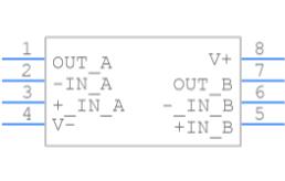
Symbol
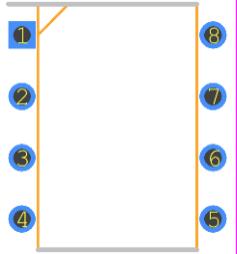
Footprint
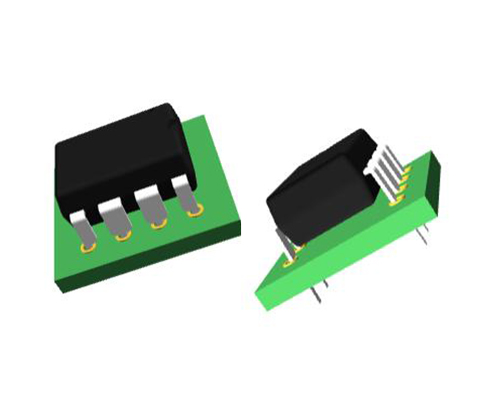
3D Models
OPA2134PA Pinout and Configurations
OPA2134PA Pinout
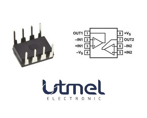
| Pin Name | NO. | I/O | DESCRIPTION |
| Out A | 1 | O | Output channel A |
| –In A | 2 | I | Inverting input channel A |
| +In A | 3 | I | Noninverting input channel A |
| V+ | 8 | - | Positive power supply |
| +In B | 5 | I | Noninverting input channel B |
| –In B | 6 | I | Inverting input channel B |
| Out B | 7 | O | Output channel B |
| Out C | - | O | Output channel C |
| –In C | - | I | Inverting input channel C |
| +In C | - | I | Noninverting input channel C |
| V– | 4 | - | Negative power supply |
| +In D | - | I | Noninverting input channel D |
| –In D | - | I | Inverting input channel D |
| Out D | - | O | Output channel D |
Specifications
- TypeParameter
- Lifecycle Status
Lifecycle Status refers to the current stage of an electronic component in its product life cycle, indicating whether it is active, obsolete, or transitioning between these states. An active status means the component is in production and available for purchase. An obsolete status indicates that the component is no longer being manufactured or supported, and manufacturers typically provide a limited time frame for support. Understanding the lifecycle status is crucial for design engineers to ensure continuity and reliability in their projects.
ACTIVE (Last Updated: 3 days ago) - Factory Lead Time6 Weeks
- Mounting Type
The "Mounting Type" in electronic components refers to the method used to attach or connect a component to a circuit board or other substrate, such as through-hole, surface-mount, or panel mount.
Through Hole - Surface Mount
having leads that are designed to be soldered on the side of a circuit board that the body of the component is mounted on.
NO - Package / Case
refers to the protective housing that encases an electronic component, providing mechanical support, electrical connections, and thermal management.
8-DIP (0.300, 7.62mm) - Number of Pins8
- Weight528.605208mg
- Number of Elements2
- Series
In electronic components, the "Series" refers to a group of products that share similar characteristics, designs, or functionalities, often produced by the same manufacturer. These components within a series typically have common specifications but may vary in terms of voltage, power, or packaging to meet different application needs. The series name helps identify and differentiate between various product lines within a manufacturer's catalog.
SoundPlus™ - Packaging
Semiconductor package is a carrier / shell used to contain and cover one or more semiconductor components or integrated circuits. The material of the shell can be metal, plastic, glass or ceramic.
Tube - Operating Temperature
The operating temperature is the range of ambient temperature within which a power supply, or any other electrical equipment, operate in. This ranges from a minimum operating temperature, to a peak or maximum operating temperature, outside which, the power supply may fail.
-40°C~85°C - JESD-609 Code
The "JESD-609 Code" in electronic components refers to a standardized marking code that indicates the lead-free solder composition and finish of electronic components for compliance with environmental regulations.
e4 - Pbfree Code
The "Pbfree Code" parameter in electronic components refers to the code or marking used to indicate that the component is lead-free. Lead (Pb) is a toxic substance that has been widely used in electronic components for many years, but due to environmental concerns, there has been a shift towards lead-free alternatives. The Pbfree Code helps manufacturers and users easily identify components that do not contain lead, ensuring compliance with regulations and promoting environmentally friendly practices. It is important to pay attention to the Pbfree Code when selecting electronic components to ensure they meet the necessary requirements for lead-free applications.
yes - Part Status
Parts can have many statuses as they progress through the configuration, analysis, review, and approval stages.
Active - Moisture Sensitivity Level (MSL)
Moisture Sensitivity Level (MSL) is a standardized rating that indicates the susceptibility of electronic components, particularly semiconductors, to moisture-induced damage during storage and the soldering process, defining the allowable exposure time to ambient conditions before they require special handling or baking to prevent failures
1 (Unlimited) - Number of Terminations8
- ECCN Code
An ECCN (Export Control Classification Number) is an alphanumeric code used by the U.S. Bureau of Industry and Security to identify and categorize electronic components and other dual-use items that may require an export license based on their technical characteristics and potential for military use.
EAR99 - Terminal Finish
Terminal Finish refers to the surface treatment applied to the terminals or leads of electronic components to enhance their performance and longevity. It can improve solderability, corrosion resistance, and overall reliability of the connection in electronic assemblies. Common finishes include nickel, gold, and tin, each possessing distinct properties suitable for various applications. The choice of terminal finish can significantly impact the durability and effectiveness of electronic devices.
Nickel/Palladium/Gold (Ni/Pd/Au) - Number of Functions2
- Supply Voltage
Supply voltage refers to the electrical potential difference provided to an electronic component or circuit. It is crucial for the proper operation of devices, as it powers their functions and determines performance characteristics. The supply voltage must be within specified limits to ensure reliability and prevent damage to components. Different electronic devices have specific supply voltage requirements, which can vary widely depending on their design and intended application.
15V - Base Part Number
The "Base Part Number" (BPN) in electronic components serves a similar purpose to the "Base Product Number." It refers to the primary identifier for a component that captures the essential characteristics shared by a group of similar components. The BPN provides a fundamental way to reference a family or series of components without specifying all the variations and specific details.
OPA2134 - Pin Count
a count of all of the component leads (or pins)
8 - Operating Supply Current
Operating Supply Current, also known as supply current or quiescent current, is a crucial parameter in electronic components that indicates the amount of current required for the device to operate under normal conditions. It represents the current drawn by the component from the power supply while it is functioning. This parameter is important for determining the power consumption of the component and is typically specified in datasheets to help designers calculate the overall power requirements of their circuits. Understanding the operating supply current is essential for ensuring proper functionality and efficiency of electronic systems.
4mA - Nominal Supply Current
Nominal current is the same as the rated current. It is the current drawn by the motor while delivering rated mechanical output at its shaft.
4mA - Slew Rate
the maximum rate of output voltage change per unit time.
20V/μs - Architecture
In electronic components, the parameter "Architecture" refers to the overall design and structure of the component. It encompasses the arrangement of internal components, the layout of circuitry, and the physical form of the component. The architecture of an electronic component plays a crucial role in determining its functionality, performance, and compatibility with other components in a system. Different architectures can result in variations in power consumption, speed, size, and other key characteristics of the component. Designers often consider the architecture of electronic components carefully to ensure optimal performance and integration within a larger system.
VOLTAGE-FEEDBACK - Amplifier Type
Amplifier Type refers to the classification or categorization of amplifiers based on their design, functionality, and characteristics. Amplifiers are electronic devices that increase the amplitude of a signal, such as voltage or current. The type of amplifier determines its specific application, performance capabilities, and operating characteristics. Common types of amplifiers include operational amplifiers (op-amps), power amplifiers, audio amplifiers, and radio frequency (RF) amplifiers. Understanding the amplifier type is crucial for selecting the right component for a particular circuit or system design.
Audio - Common Mode Rejection Ratio
Common Mode Rejection Ratio (CMRR) is a measure of the ability of a differential amplifier to reject input signals that are common to both input terminals. It is defined as the ratio of the differential gain to the common mode gain. A high CMRR indicates that the amplifier can effectively eliminate noise and interference that affects both inputs simultaneously, enhancing the fidelity of the amplified signal. CMRR is typically expressed in decibels (dB), with higher values representing better performance in rejecting common mode signals.
86 dB - Current - Input Bias
The parameter "Current - Input Bias" in electronic components refers to the amount of current required at the input terminal of a device to maintain proper operation. It is a crucial specification as it determines the minimum input current needed for the component to function correctly. Input bias current can affect the performance and accuracy of the device, especially in precision applications where small signal levels are involved. It is typically specified in datasheets for operational amplifiers, transistors, and other semiconductor devices to provide users with important information for circuit design and analysis.
5pA - Voltage - Supply, Single/Dual (±)
The parameter "Voltage - Supply, Single/Dual (±)" in electronic components refers to the power supply voltage required for the proper operation of the component. This parameter indicates whether the component requires a single power supply voltage (e.g., 5V) or a dual power supply voltage (e.g., ±15V). For components that require a single power supply voltage, only one voltage level is needed for operation. On the other hand, components that require a dual power supply voltage need both positive and negative voltage levels to function correctly.Understanding the voltage supply requirements of electronic components is crucial for designing and integrating them into circuits to ensure proper functionality and prevent damage due to incorrect voltage levels.
5V~36V ±2.5V~18V - Output Current per Channel
Output Current per Channel is a specification commonly found in electronic components such as amplifiers, audio interfaces, and power supplies. It refers to the maximum amount of electrical current that can be delivered by each individual output channel of the component. This parameter is important because it determines the capacity of the component to drive connected devices or loads. A higher output current per channel means the component can deliver more power to connected devices, while a lower output current may limit the performance or functionality of the component in certain applications. It is crucial to consider the output current per channel when selecting electronic components to ensure they can meet the power requirements of the intended system or setup.
35mA - Supply Type
Supply Type in electronic components refers to the classification of power sources used to operate the component. It indicates whether the component requires DC or AC power, and if DC, specifies the voltage levels such as low, medium, or high. Different supply types can affect the performance, compatibility, and application of the component in electronic circuits. Understanding the supply type is crucial for proper component selection and integration into electronic designs.
Dual - Input Offset Voltage (Vos)
Input Offset Voltage (Vos) is a key parameter in electronic components, particularly in operational amplifiers. It refers to the voltage difference that must be applied between the two input terminals of the amplifier to nullify the output voltage when the input terminals are shorted together. In simpler terms, it represents the voltage required to bring the output of the amplifier to zero when there is no input signal present. Vos is an important parameter as it can introduce errors in the output signal of the amplifier, especially in precision applications where accuracy is crucial. Minimizing Vos is essential to ensure the amplifier operates with high precision and accuracy.
500μV - Neg Supply Voltage-Nom (Vsup)
The parameter "Neg Supply Voltage-Nom (Vsup)" in electronic components refers to the nominal negative supply voltage that the component requires to operate within its specified performance characteristics. This parameter indicates the minimum voltage level that must be provided to the component's negative supply pin for proper functionality. It is important to ensure that the negative supply voltage provided to the component does not exceed the maximum specified value to prevent damage or malfunction. Understanding and adhering to the specified negative supply voltage requirements is crucial for the reliable operation of the electronic component in a circuit.
-15V - Unity Gain BW-Nom
Unity Gain Bandwidth, often abbreviated as Unity Gain BW or UGBW, refers to the frequency at which an amplifier can provide a gain of one (0 dB). It is a critical parameter in assessing the performance of operational amplifiers and other amplifying devices, indicating the range of frequencies over which the amplifier can operate without distortion. Unity Gain BW is particularly important in applications where signal fidelity is crucial, as it helps determine the maximum frequency of operation for a given gain level. As the gain is reduced, the bandwidth typically increases, ensuring that the amplifier can still operate effectively across various signal frequencies.
8000 kHz - Voltage Gain
Voltage gain is a measure of how much an electronic component or circuit amplifies an input voltage signal to produce an output voltage signal. It is typically expressed as a ratio or in decibels (dB). A higher voltage gain indicates a greater amplification of the input signal. Voltage gain is an important parameter in amplifiers, where it determines the level of amplification provided by the circuit. It is calculated by dividing the output voltage by the input voltage and is a key factor in determining the overall performance and functionality of electronic devices.
120dB - Average Bias Current-Max (IIB)
The parameter "Average Bias Current-Max (IIB)" in electronic components refers to the maximum average bias current that the component can handle without exceeding its specified operating limits. Bias current is the current that flows through a component when it is in its quiescent state or when it is not actively processing a signal. Exceeding the maximum average bias current can lead to overheating, reduced performance, or even damage to the component. Therefore, it is important to ensure that the bias current does not exceed the specified maximum value to maintain the reliability and longevity of the electronic component.
0.0001μA - Power Supply Rejection Ratio (PSRR)
Power Supply Rejection Ratio (PSRR) is a measure of how well an electronic component, such as an operational amplifier or voltage regulator, can reject changes in its supply voltage. It indicates the ability of the component to maintain a stable output voltage despite fluctuations in the input supply voltage. A higher PSRR value signifies better performance in rejecting noise and variations from the power supply, leading to improved signal integrity and more reliable operation in electronic circuits. PSRR is typically expressed in decibels (dB).
90dB - Low-Offset
Low-offset is a parameter used to describe the level of offset voltage in electronic components, particularly in operational amplifiers. Offset voltage refers to the small voltage difference that exists between the input terminals of the amplifier when the input voltage is zero. A low-offset value indicates that this voltage difference is minimal, which is desirable for accurate signal processing and amplification. Components with low-offset specifications are preferred in applications where precision and accuracy are critical, such as in instrumentation and measurement systems. Minimizing offset voltage helps reduce errors and ensures the faithful reproduction of input signals by the amplifier.
NO - Frequency Compensation
Frequency compensation is implemented by modifying the gain and phase characteristics of the amplifier's open loop output or of its feedback network, or both, in such a way as to avoid the conditions leading to oscillation. This is usually done by the internal or external use of resistance-capacitance networks.
YES - Low-Bias
Low-bias in electronic components refers to a design or configuration that minimizes the amount of bias current flowing through the component. Bias current is a small, steady current that is used to establish the operating point of a component, such as a transistor or amplifier. By reducing the bias current to a low level, the component can operate with lower power consumption and potentially lower distortion. Low-bias components are often used in applications where power efficiency and signal fidelity are important, such as in audio amplifiers or battery-powered devices. Overall, the low-bias parameter indicates the ability of the component to operate efficiently and accurately with minimal bias current.
YES - Micropower
the use of very small electric generators and prime movers or devices to convert heat or motion to electricity, for use close to the generator.
NO - Bias Current-Max (IIB) @25C
The parameter "Bias Current-Max (IIB) @25C" in electronic components refers to the maximum input bias current that the component can handle at a specified temperature of 25 degrees Celsius. Bias current is the current flowing into the input terminal of a device when no signal is applied. This parameter is important because excessive bias current can affect the performance and stability of the component, leading to potential issues such as distortion or offset errors in the output signal. By specifying the maximum bias current allowed at a certain temperature, manufacturers provide users with important information to ensure proper operation and reliability of the component in their circuit designs.
0.0001μA - Programmable Power
A programmable power supply provides remote control capability of the output voltage(s) via an analog control signal controlled by keypad or rotary switch from the front panel of the power supply or via a computer interface such as RS232, GPIB, or USB.
NO - Dual Supply Voltage
Dual Supply Voltage refers to an electronic component's requirement for two separate power supply voltages, typically one positive and one negative. This configuration is commonly used in operational amplifiers, analog circuits, and certain digital devices to allow for greater signal handling capabilities and improved performance. The use of dual supply voltages enables the device to process bipolar signals, thereby enhancing its functionality in various applications.
9V - Nominal Gain Bandwidth Product
The Nominal Gain Bandwidth Product is a key parameter in electronic components, particularly in operational amplifiers. It represents the product of the gain and the bandwidth at which that gain is achieved. In simpler terms, it indicates the frequency range over which the amplifier can provide a specified level of gain. A higher Nominal Gain Bandwidth Product implies that the amplifier can operate over a wider range of frequencies while maintaining a consistent level of amplification. Designers often consider this parameter when selecting components for applications that require specific bandwidth and gain requirements.
8MHz - Input Offset Current-Max (IIO)
Input Offset Current-Max (IIO) is a parameter that describes the maximum difference in input bias currents between two input terminals of an electronic component, such as an operational amplifier. Input offset current can cause errors in the output of the component, especially in precision applications where accuracy is crucial. The IIO specification provides a limit on the maximum allowable difference in input currents to ensure that the component operates within its specified performance range. Designers need to consider the IIO value when selecting components and designing circuits to minimize errors and ensure reliable operation.
0.00005μA - Load Impedance
Load impedance is a crucial parameter in electronic components that refers to the impedance presented by the load to the output of a circuit or device. It is a measure of how much the load resists the flow of current from the source. Load impedance is typically expressed in ohms and can greatly affect the performance and efficiency of a circuit. Matching the load impedance to the source impedance is important for maximum power transfer and signal integrity in electronic systems. Failure to properly match load impedance can result in signal distortion, power loss, and reduced overall performance of the circuit.
2kOhm - Height5.08mm
- Length9.81mm
- Width6.35mm
- Thickness
Thickness in electronic components refers to the measurement of how thick a particular material or layer is within the component structure. It can pertain to various aspects, such as the thickness of a substrate, a dielectric layer, or conductive traces. This parameter is crucial as it impacts the electrical, mechanical, and thermal properties of the component, influencing its performance and reliability in electronic circuits.
3.9mm - RoHS Status
RoHS means “Restriction of Certain Hazardous Substances” in the “Hazardous Substances Directive” in electrical and electronic equipment.
ROHS3 Compliant - Radiation Hardening
Radiation hardening is the process of making electronic components and circuits resistant to damage or malfunction caused by high levels of ionizing radiation, especially for environments in outer space (especially beyond the low Earth orbit), around nuclear reactors and particle accelerators, or during nuclear accidents or nuclear warfare.
No - REACH SVHC
The parameter "REACH SVHC" in electronic components refers to the compliance with the Registration, Evaluation, Authorization, and Restriction of Chemicals (REACH) regulation regarding Substances of Very High Concern (SVHC). SVHCs are substances that may have serious effects on human health or the environment, and their use is regulated under REACH to ensure their safe handling and minimize their impact.Manufacturers of electronic components need to declare if their products contain any SVHCs above a certain threshold concentration and provide information on the safe use of these substances. This information allows customers to make informed decisions about the potential risks associated with using the components and take appropriate measures to mitigate any hazards.Ensuring compliance with REACH SVHC requirements is essential for electronics manufacturers to meet regulatory standards, protect human health and the environment, and maintain transparency in their supply chain. It also demonstrates a commitment to sustainability and responsible manufacturing practices in the electronics industry.
No SVHC - Lead Free
Lead Free is a term used to describe electronic components that do not contain lead as part of their composition. Lead is a toxic material that can have harmful effects on human health and the environment, so the electronics industry has been moving towards lead-free components to reduce these risks. Lead-free components are typically made using alternative materials such as silver, copper, and tin. Manufacturers must comply with regulations such as the Restriction of Hazardous Substances (RoHS) directive to ensure that their products are lead-free and environmentally friendly.
Lead Free
OPA2134PA Features
1. Superior Sound Quality
2. Ultra-Low Distortion: 0.00008%
3. Low Noise: 8 nV/√Hz
4. True FET-Input: IB = 5pA
5. High Speed:
-Slew Rate: 20 V/µs
-Bandwidth: 8 MHz
6. High Open-Loop Gain: 120 dB (600 Ω)
7. Wide Supply Range: ±2.5 V to ±18 V
OPA2134P Applications
• Professional Audio and Music
• Line Drivers
• Line Receivers
• Multimedia Audio
•Active Filters
• Preamplifiers
• Integrator
• Crossover Networks
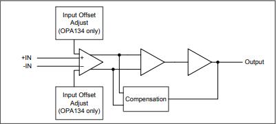
OPA2134PA Functional Block Diagram
OPA2134PA Dimensions
| Dimensions | |
| Height | 5.08 mm |
| Length | 9.81 mm |
| Thickness | 3.9 mm |
| Width | 6.35 mm |
OPA2134PA Substitutes
| Part No. | Manufacturer |
| MUSES02 | Nisshinbo Micro Devices Inc. |
| LT1113CN8#PBF | Analog Devices Inc. |
| NJM5532D | Nisshinbo Micro Devices Inc. |
| LT1113ACN8#PBF | Analog Devices Inc. |
| NJM4558D | Nisshinbo Micro Devices Inc. |
| NJM4580D | Nisshinbo Micro Devices Inc. |
| AD746JNZ | Analog Devices Inc. |
| LT1169CN8#PBF | Analog Devices Inc. |
| NJM2068D | Nisshinbo Micro Devices Inc. |
| OPA4132UA | TEXAS INSTRUMENTS |
OPA2134PA Manufacturer
Texas Instruments Incorporated (TI) is an American technology company headquartered in Dallas, Texas, that designs and manufactures semiconductors and various integrated circuits, which it sells to electronics designers and manufacturers globally. It is one of the top 10 semiconductor companies worldwide based on sales volume. The company's focus is on developing analog chips and embedded processors, which account for more than 80% of its revenue. TI also produces TI digital light processing technology and education technology products including calculators, microcontrollers, and multi-core processors.
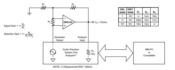
OPA2134PA Distortion Measurements
The distortion produced by the OPA134 series of operational amplifiers is below the measurement limit of all known commercially-available equipment. However, a special test circuit can extend the measurement capabilities. Operational amplifier distortion can be considered an internal error source that can be referred to as the input.
OPA2134PA vs OPA2134UA
OPA2134PA and OPA2134UA are similar in many aspects. Their differences can be concluded in the following chart.
| OPA2134PA | OPA2134UA | |
| Part Package Code | DIP | SOIC |
| JESD-30 Code | R-PDIP-T8 | R-PDSO-G8 |
| Length | 9.56 mm | 4.905 mm |
| Package Code | DIP | SOP |
| Package Style | IN-LINE | SMALL OUTLINE |
| Seated Height-Max | 5.08 mm | 1.75 mm |
| Surface Mount | NO | YES |
| Terminal Pitch | 2.54 mm | 1.27 mm |
| Width | 7.62 mm | 3.895 mm |
| Base Number Matches | 2 | 5 |
OPA2134PA Using Warnings
Please check their parameters and pin configuration before replacing them in your circuit. So customers are responsible for determining the suitability of components for their purposes.
OPA2134PA Datasheet
OPA2134PA Package
DIP-8

Trend Analysis
Datasheet PDF
- PCN Assembly/Origin :
Parts with Similar Specs
- ImagePart NumberManufacturerPackage / CaseNumber of PinsSlew RateInput Offset Voltage (Vos)Common Mode Rejection RatioSupply VoltageOperating Supply CurrentNumber of TerminationsView Compare
![OPA2134PA]()
OPA2134PA
8-DIP (0.300, 7.62mm)
8
20V/μs
500 μV
86 dB
15 V
4 mA
8
![TLC072CP]()
8-DIP (0.300, 7.62mm)
8
20V/μs
500 μV
86 dB
15 V
4 mA
8
![OPA2132PA]()
8-DIP (0.300, 7.62mm)
8
19V/μs
390 μV
80 dB
5 V
2.1 mA
8
![TLC072IP]()
8-DIP (0.300, 7.62mm)
8
19V/μs
1.9 mV
80 dB
5 V
2.1 mA
8

What is the Operating Temperature Max of OPA2134PA?
85°C
How many pins does OPA2134PA have?
8 pins
What is the Operating Temperature Min of OPA2134PA?
-40°C
What is the Bandwidth of OPA2134PA?
8MHz
What is the No. of Channels of OPA2134PA?
2 Channel
 SHT15 Humidity Sensor: Datasheet, Pinout and Features
06 September 20212512
 TL072 vs JRC4558 vs NE5532:How to differentiate?
15 April 202239702
 1N4005 Diode: Datasheet, Pinout, and Equivalents
30 August 202111585
 STM32MP157CAA3 Development: From Setup and Configuration to Advanced Features Implementation
07 June 20251338
 IRFP460 MOSFET: IRFP460 vs.IRFP460A, Pinout and Equivalent
28 March 202216924
 LM311D Linear Comparator: Feature, Specification, and Datasheet
09 June 20213726
 BC556 PNP Transistor: Pinout, Datasheet, and Equivalent
13 August 20216130
 MIC4452YN IC GATE DRVR LOW-SIDE 8DIP: Datasheet, Pinout, and Equivalents
14 February 20221647
 Three Phase Inverter - 180 Degree Conduction Mode
05 October 202320897
 Efficiency-Related Issues in GaN and SiC Power Systems
06 February 20233769
 What is a Ground Fault Circuit Interrupter?
27 March 20255575
 NOR Flash: Working, Structure and Applications
18 November 202114688
 What is SPI (Serial Perripheral Interface)?
25 November 20215066
 Top 5 SR44 Battery Brands for Reliable Power
20 August 20254811
 Towards an Optoelectronic Chip That Mimics the Human Brain
20 April 2022944
 Substitute Part Validation: How to Cross-Reference and Verify Obsolete Components
04 June 2026168
Texas Instruments
In Stock
Minimum: 1 Multiples: 1
Qty
Unit Price
Ext Price
1
$4.854966
$4.85
10
$4.580157
$45.80
100
$4.320902
$432.09
500
$4.076323
$2,038.16
1000
$3.845588
$3,845.59
Not the price you want? Send RFQ Now and we'll contact you ASAP.
Inquire for More Quantity
![LMV722MX]() LMV722MX
LMV722MXTexas Instruments
![LMC6082AIN]() LMC6082AIN
LMC6082AINTexas Instruments
![RC4558P]() RC4558P
RC4558PTexas Instruments
![LMC6482IMM/NOPB]() LMC6482IMM/NOPB
LMC6482IMM/NOPBTexas Instruments
![LM324MX/NOPB]() LM324MX/NOPB
LM324MX/NOPBTexas Instruments
![LM324AM/NOPB]() LM324AM/NOPB
LM324AM/NOPBTexas Instruments
![LMV324IDR]() LMV324IDR
LMV324IDRTexas Instruments
![LMC7101BIM5/NOPB]() LMC7101BIM5/NOPB
LMC7101BIM5/NOPBTexas Instruments
![TLV2372IDR]() TLV2372IDR
TLV2372IDRTexas Instruments
![NE5532P]() NE5532P
NE5532PTexas Instruments


