
 Product
 Brand
Brand Articles
 Tools
Tools
SI5351 Clock Generator: Datasheet, Pinout and Applications

2.5V Clock Generator SI5351 Clock Generators MultiSynth™ Series 20-VFQFN Exposed Pad 20 Terminals Surface Mount 1.71V~3.6V Tray
Unit Price: $2.524812
Ext Price: $2.52


2.5V Clock Generator SI5351 Clock Generators MultiSynth™ Series 20-VFQFN Exposed Pad 20 Terminals Surface Mount 1.71V~3.6V Tray
The Si5351 is an I2C configurable clock generator that is ideally suited for replacing crystals, crystal oscillators, VCXOs, phase-locked loops (PLLs), and fanout buffers in cost-sensitive applications. This article mainly covers datasheet, pinout, applications, features, and other details about Si5351.

Adafruit Si5351 breakout board
SI5351 Pinout


SI5351 CAD Model
Symbol

Footprint

3D Model

SI5351 Description
The Si5351 is an I2C configurable clock generator that is ideally suited for replacing crystals, crystal oscillators, VCXOs, phase-locked loops (PLLs), and fanout buffers in cost-sensitive applications. Based on PLL/VCXO + high-resolution MultiSynth fractional divider architecture, the Si5351 can generate any frequency up to 200 MHz on each of its outputs with 0 ppm error.
Specifications
- TypeParameter
- Factory Lead Time6 Weeks
- Mounting Type
The "Mounting Type" in electronic components refers to the method used to attach or connect a component to a circuit board or other substrate, such as through-hole, surface-mount, or panel mount.
Surface Mount - Package / Case
refers to the protective housing that encases an electronic component, providing mechanical support, electrical connections, and thermal management.
20-VFQFN Exposed Pad - Surface Mount
having leads that are designed to be soldered on the side of a circuit board that the body of the component is mounted on.
YES - Number of Pins20
- Operating Temperature
The operating temperature is the range of ambient temperature within which a power supply, or any other electrical equipment, operate in. This ranges from a minimum operating temperature, to a peak or maximum operating temperature, outside which, the power supply may fail.
-40°C~85°C - Packaging
Semiconductor package is a carrier / shell used to contain and cover one or more semiconductor components or integrated circuits. The material of the shell can be metal, plastic, glass or ceramic.
Tray - Series
In electronic components, the "Series" refers to a group of products that share similar characteristics, designs, or functionalities, often produced by the same manufacturer. These components within a series typically have common specifications but may vary in terms of voltage, power, or packaging to meet different application needs. The series name helps identify and differentiate between various product lines within a manufacturer's catalog.
MultiSynth™ - Published2000
- Part Status
Parts can have many statuses as they progress through the configuration, analysis, review, and approval stages.
Active - Moisture Sensitivity Level (MSL)
Moisture Sensitivity Level (MSL) is a standardized rating that indicates the susceptibility of electronic components, particularly semiconductors, to moisture-induced damage during storage and the soldering process, defining the allowable exposure time to ambient conditions before they require special handling or baking to prevent failures
2 (1 Year) - Number of Terminations20
- ECCN Code
An ECCN (Export Control Classification Number) is an alphanumeric code used by the U.S. Bureau of Industry and Security to identify and categorize electronic components and other dual-use items that may require an export license based on their technical characteristics and potential for military use.
EAR99 - TypeClock Generator
- Additional Feature
Any Feature, including a modified Existing Feature, that is not an Existing Feature.
ALSO OPERATES AT 3.3 V SUPPLY - Voltage - Supply
Voltage - Supply refers to the range of voltage levels that an electronic component or circuit is designed to operate with. It indicates the minimum and maximum supply voltage that can be applied for the device to function properly. Providing supply voltages outside this range can lead to malfunction, damage, or reduced performance. This parameter is critical for ensuring compatibility between different components in a circuit.
1.71V~3.6V - Terminal Position
In electronic components, the term "Terminal Position" refers to the physical location of the connection points on the component where external electrical connections can be made. These connection points, known as terminals, are typically used to attach wires, leads, or other components to the main body of the electronic component. The terminal position is important for ensuring proper connectivity and functionality of the component within a circuit. It is often specified in technical datasheets or component specifications to help designers and engineers understand how to properly integrate the component into their circuit designs.
QUAD - Terminal Form
Occurring at or forming the end of a series, succession, or the like; closing; concluding.
NO LEAD - Peak Reflow Temperature (Cel)
Peak Reflow Temperature (Cel) is a parameter that specifies the maximum temperature at which an electronic component can be exposed during the reflow soldering process. Reflow soldering is a common method used to attach electronic components to a circuit board. The Peak Reflow Temperature is crucial because it ensures that the component is not damaged or degraded during the soldering process. Exceeding the specified Peak Reflow Temperature can lead to issues such as component failure, reduced performance, or even permanent damage to the component. It is important for manufacturers and assemblers to adhere to the recommended Peak Reflow Temperature to ensure the reliability and functionality of the electronic components.
260 - Supply Voltage
Supply voltage refers to the electrical potential difference provided to an electronic component or circuit. It is crucial for the proper operation of devices, as it powers their functions and determines performance characteristics. The supply voltage must be within specified limits to ensure reliability and prevent damage to components. Different electronic devices have specific supply voltage requirements, which can vary widely depending on their design and intended application.
2.5V - Terminal Pitch
The center distance from one pole to the next.
0.5mm - Frequency
In electronic components, the parameter "Frequency" refers to the rate at which a signal oscillates or cycles within a given period of time. It is typically measured in Hertz (Hz) and represents how many times a signal completes a full cycle in one second. Frequency is a crucial aspect in electronic components as it determines the behavior and performance of various devices such as oscillators, filters, and communication systems. Understanding the frequency characteristics of components is essential for designing and analyzing electronic circuits to ensure proper functionality and compatibility with other components in a system.
200MHz - Time@Peak Reflow Temperature-Max (s)
Time@Peak Reflow Temperature-Max (s) refers to the maximum duration that an electronic component can be exposed to the peak reflow temperature during the soldering process, which is crucial for ensuring reliable solder joint formation without damaging the component.
30 - Base Part Number
The "Base Part Number" (BPN) in electronic components serves a similar purpose to the "Base Product Number." It refers to the primary identifier for a component that captures the essential characteristics shared by a group of similar components. The BPN provides a fundamental way to reference a family or series of components without specifying all the variations and specific details.
SI5351 - Output
In electronic components, the parameter "Output" typically refers to the signal or data that is produced by the component and sent to another part of the circuit or system. The output can be in the form of voltage, current, frequency, or any other measurable quantity depending on the specific component. The output of a component is often crucial in determining its functionality and how it interacts with other components in the circuit. Understanding the output characteristics of electronic components is essential for designing and troubleshooting electronic circuits effectively.
LVCMOS - Number of Outputs8
- Number of Circuits2
- Operating Supply Current
Operating Supply Current, also known as supply current or quiescent current, is a crucial parameter in electronic components that indicates the amount of current required for the device to operate under normal conditions. It represents the current drawn by the component from the power supply while it is functioning. This parameter is important for determining the power consumption of the component and is typically specified in datasheets to help designers calculate the overall power requirements of their circuits. Understanding the operating supply current is essential for ensuring proper functionality and efficiency of electronic systems.
45mA - Input
In electronic components, "Input" refers to the signal or data that is provided to a device or system for processing or manipulation. It is the information or command that is received by the component to initiate a specific function or operation. The input can come from various sources such as sensors, other electronic devices, or user interactions. It is crucial for the proper functioning of the component as it determines how the device will respond or behave based on the input received. Understanding and managing the input parameters is essential in designing and using electronic components effectively.
Crystal - Ratio - Input:Output
The parameter "Ratio - Input:Output" in electronic components refers to the relationship between the input and output quantities of a device or system. It is a measure of how the input signal or energy is transformed or converted into the output signal or energy. This ratio is often expressed as a numerical value or percentage, indicating the efficiency or effectiveness of the component in converting the input to the desired output. A higher ratio typically signifies better performance or higher efficiency, while a lower ratio may indicate losses or inefficiencies in the conversion process. Understanding and optimizing the input-output ratio is crucial in designing and evaluating electronic components for various applications.
1:8 - Primary Clock/Crystal Frequency-Nom
The parameter "Primary Clock/Crystal Frequency-Nom" refers to the nominal frequency at which a clock or crystal oscillator operates in electronic components. This frequency is critical for synchronizing the timing of various processes within a circuit or system. It is typically specified in hertz and indicates the standard or average frequency that the oscillator is designed to achieve under normal operating conditions. Accurate frequency is essential for ensuring proper functioning and performance of digital circuits and communication systems.
27MHz - PLL
PLL stands for Phase-Locked Loop, which is a control system that generates an output signal whose phase is related to the phase of an input signal. It is commonly used in electronic components to synchronize, modulate, demodulate, filter, or recover a signal's frequency. A PLL typically consists of a phase detector, a loop filter, a voltage-controlled oscillator (VCO), and a feedback circuit. The PLL locks the phase of the output signal to the phase of the input signal, making it a versatile tool in various applications such as frequency synthesis, clock recovery, and frequency modulation.
Yes - Differential - Input:Output
Differential - Input:Output refers to the relationship between the input and output signals in differential amplifiers or circuits. It measures the difference in voltage between two input terminals and produces an output that is proportional to this difference. This parameter is essential for noise rejection and improving signal integrity in various applications, such as operational amplifiers and data acquisition systems. It allows circuits to effectively amplify small signals while minimizing interference and common-mode noise.
No/No - Max Duty Cycle
Max Duty Cycle refers to the maximum percentage of time that an electronic component, such as a switch or a power supply, can be in an "on" state during a defined time period. It is an important parameter in pulse-width modulated (PWM) systems and helps determine how often a device can operate without overheating or sustaining damage. By specifying the maximum duty cycle, manufacturers provide guidance on the safe operational limits of the component, ensuring reliability and efficiency in various applications.
55 % - Divider/Multiplier
The parameter "Divider/Multiplier" in electronic components refers to a feature that allows the component to divide or multiply an input signal by a certain factor. This feature is commonly found in components such as operational amplifiers, voltage regulators, and signal processing circuits. In the context of operational amplifiers, the Divider/Multiplier parameter indicates the ability of the amplifier to scale the input signal by a specific factor, either dividing it or multiplying it. This can be useful for adjusting the amplitude or gain of a signal in a circuit.Overall, the Divider/Multiplier parameter provides flexibility in signal processing applications by allowing users to manipulate the input signal according to their specific requirements, whether it involves scaling down the signal for further processing or amplifying it for increased output.
Yes/No - Height850μm
- Length4mm
- Width4mm
- RoHS Status
RoHS means “Restriction of Certain Hazardous Substances” in the “Hazardous Substances Directive” in electrical and electronic equipment.
RoHS Compliant - Lead Free
Lead Free is a term used to describe electronic components that do not contain lead as part of their composition. Lead is a toxic material that can have harmful effects on human health and the environment, so the electronics industry has been moving towards lead-free components to reduce these risks. Lead-free components are typically made using alternative materials such as silver, copper, and tin. Manufacturers must comply with regulations such as the Restriction of Hazardous Substances (RoHS) directive to ensure that their products are lead-free and environmentally friendly.
Lead Free
SI5351 Functional Block Diagram

SI5351 Features
Generates up to eight non-interrelated frequencies from 2.5 kHz to 200 MHz
I2C user-definable configuration
Exact frequency synthesis at each output (0 ppm error)
Highly linear VCXO
The optional clock input (CLKIN)
Low output period jitter: < 70 ps pp, typ
Configurable spread spectrum selectable at each output
Operates from a low-cost, fixed frequency crystal: 25 or 27 MHz
Supports static phase offset
Programmable rise/fall time control
Glitch fewer frequency changes
Separate voltage supply pins provide the level translation:
Core VDD: 2.5 or 3.3 V
Output VDDO: 1.8, 2.5, or 3.3 V
Excellent PSRR eliminates external power supply filtering
Very low power consumption
Adjustable output delay
Available in three packages types:
10-MSOP: 3 outputs
16-QFN (3x3 mm): 4 outputs
20-QFN (4x4 mm): 8 outputs
PCIe Gen 1 compatible
Supports HCSL compatible swing
SI5351 Applications
Audio/video equipment, gaming
Printers, scanners, projectors
Handheld Instrumentation
Laser range finder
Residential gateways
Networking/communication
Servers, storage
XO replacement
SI5351 Alternatives

SI5351 Package


SI5351 Manufacturer
Silicon Labs is a leader in secure, intelligent wireless technology for a more connected world. Our integrated hardware and software platform, intuitive development tools, unmatched ecosystem, and robust support make us the ideal long-term partner in building advanced industrial, commercial, home, and life applications. We make it easy for developers to solve complex wireless challenges throughout the product lifecycle and get to market quickly with innovative solutions that transform industries, grow economies and improve lives.
Trend Analysis
Datasheet PDF
- Datasheets :
- PCN Packaging :
- PCN Design/Specification :
- PCN Assembly/Origin :
What is SI5351 used for?
The Si5351 is an I2C configurable clock generator that is ideally suited for replacing crystals, crystal oscillators, VCXOs, phase-locked loops (PLLs), and fanout buffers in cost-sensitive applications.
How does SI5351 work?
The Si5351 clock generator is an I2C controller clock generator. It uses the onboard precision clock to drive multiple PLL's and clock dividers using I2C instructions. By setting up the PLL and dividers you can create precise and arbitrary frequencies.
 Designing Ultra-Compact Electronics with ATTINY10: Specs, Pinout, and TPI Programming
06 February 2026100
 MJE340 Transistor:Pinout, Equivalent, Datasheet
04 December 20218120
 DAC0808 D/A converter IC: Alternatives, Pinout and Working principle
16 September 202110663
 CD4046BE Micropower Phase-Locked Loop: Pinout and Datasheet
30 March 20225941
 ISO1050DUB Isolated CAN Transceiver: Pinout, Specification, and Datasheet
07 July 20213327
 KSP2222A NPN Transistor: Pinout, Datasheet and Equivalents
03 November 20217409
![RG8 VS LMR400[FAQ]: Differentiate the differences between them.](https://res.utmel.com/Images/Article/001960bf-022b-4557-968e-67dcf2b7c44f.png) RG8 VS LMR400[FAQ]: Differentiate the differences between them.
RG8 VS LMR400[FAQ]: Differentiate the differences between them.12 June 202421653
 74HC74 Dual D Flip-Flop: Datasheet pdf, Pinout and Flip-Flop Diagram
17 December 202115512
 An Overview of Photoelectric Sensors
27 October 20258516
 The World's Top 10 Innovative LED Drivers
12 February 20224274
 What is Conductivity Sensor?
20 June 202211114
 What is an Electrical Connector?
19 November 20258053
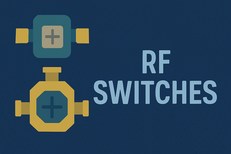 RF Switches Guide: Types, Specifications & Applications
03 July 20253480
 How much do you know about CPU?
07 February 20222516
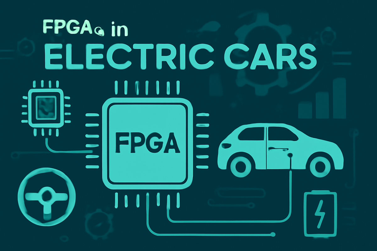 FPGAs in the Electric Cars: The Complete Guide to Powertrain, ADAS, and BMS
25 August 20252136
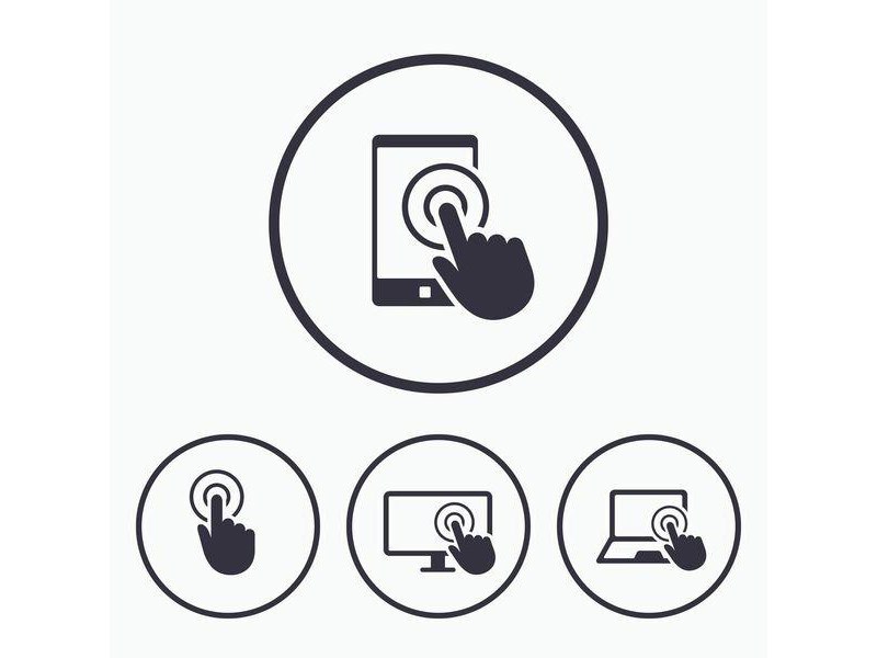 Working and Types of Touch Screen
20 March 20215858
Silicon Labs
In Stock
Minimum: 1 Multiples: 1
Qty
Unit Price
Ext Price
1
$2.524812
$2.52
10
$2.381898
$23.82
100
$2.247074
$224.71
500
$2.119881
$1,059.94
1000
$1.999888
$1,999.89
Not the price you want? Send RFQ Now and we'll contact you ASAP.
Inquire for More Quantity
![SI5310-BM]() SI5310-BM
SI5310-BMSilicon Labs
![SI5342B-D-GM]() SI5342B-D-GM
SI5342B-D-GMSilicon Labs
![SI51214-A1FAGMR]() SI51214-A1FAGMR
SI51214-A1FAGMRSilicon Labs
![SI5351A-B-GTR]() SI5351A-B-GTR
SI5351A-B-GTRSilicon Labs
![SI5326B-C-GM]() SI5326B-C-GM
SI5326B-C-GMSilicon Labs
![SI5351B-B-GM]() SI5351B-B-GM
SI5351B-B-GMSilicon Labs
![SI5351A-B-GT]() SI5351A-B-GT
SI5351A-B-GTSilicon Labs
![SI5351C-B-GMR]() SI5351C-B-GMR
SI5351C-B-GMRSilicon Labs
![SI5326B-C-GMR]() SI5326B-C-GMR
SI5326B-C-GMRSilicon Labs


