
 Product
 Brand
Brand Articles
 Tools
Tools
TCA9548APWR I2C Switch: Circuit, Pinout, and Datasheet

24 Terminations 1.65V~5.5V 24 Pin CA9548 Signal switch TCA Series 8 Outputs 1 Functions


24 Terminations 1.65V~5.5V 24 Pin CA9548 Signal switch TCA Series 8 Outputs 1 Functions
The TCA9548APWR is a bidirectional translating I2C switch with eight channels. This article mainly introduces Circuit, Pinout, Datasheet and other detailed information about Texas Instruments TCA9548APWR.

TCA9548A I2C Multiplexer: Use Multiple Devices with the Same Address on Arduino
- TCA9548APWR Description
- TCA9548APWR Pinout
- TCA9548APWR CAD Model
- TCA9548APWR Features
- Specifications
- Parts with Similar Specs
- TCA9548APWR Functional Block Diagram
- TCA9548APWR Typical Application
- TCA9548APWR Circuit Diagram
- TCA9548APWR Simplified Application Diagram
- TCA9548APWR Layout
- TCA9548APWR Alternatives
- TCA9548APWR Applications
- TCA9548APWR Package
- TCA9548APWR Manufacturer
- Trend Analysis
- Datasheet PDF
TCA9548APWR Description
The TCA9548APWR is a bidirectional translating I2C switch with eight channels. SC0/SD0-SC7/SD7 are the slave devices that receive the master SCL/SDA signal pair. Any of the eight downstream channels, as well as any combination of them, can be chosen.
The TCA9548APWR includes an active-low RESET input that resets the state machine and helps the device to recover if one of the downstream I2C buses becomes stuck in a low state. The device's state machine can also be reset by cycling the power supply, commonly known as a power-on reset, by cycling the power supply, VCC (POR). All channels are deselected when you use the RESET function or a POR.
The I2C data path connections are controlled by a single I2C master device that can communicate with numerous I2C slaves. After the slave address (hardware selectable by A0, A1, and A2 pins) is successfully acknowledged, a single 8-bit control register is written to or read from to determine the preferred channels.
The TCA9548APWR can also be used for voltage translation, letting 1.8-V, 2.5-V, or 3.3-V parts interact with 5-V parts by using various bus voltages on each SCn/SDn pair. External pull-up resistors are used to bring the bus up to the desired voltage for both the master and slave channels.
TCA9548APWR Pinout
The following figure shows TCA9548APWR Pinout.

Pinout
| Pin Number | Pin Name | Description |
| 1 | A0 | Address input 0. Connect directly to VCC or ground |
| 2 | A1 | Address input 1. Connect directly to VCC or ground |
| 21 | A2 | Address input 2. Connect directly to VCC or ground |
| 12 | GND | Ground |
| 3 | RESET | Active-low reset input. Connect to VCC or VDPUM through a pull-up resistor, if not used |
| 4 | SD0 | Serial data 0. Connect to VDPU0 through a pull-up resistor |
| 5 | SC0 | Serial clock 0. Connect to VDPU0 through a pull-up resistor |
| 6 | SD1 | Serial data 1. Connect to VDPU1 through a pull-up resistor |
| 7 | SC1 | Serial clock 1. Connect to VDPU1 through a pull-up resistor |
| 8 | SD2 | Serial data 2. Connect to VDPU2 through a pull-up resistor |
| 9 | SC2 | Serial clock 2. Connect to VDPU2 through a pull-up resistor |
| 10 | SD3 | Serial data 3. Connect to VDPU3 through a pull-up resistor |
| 11 | SC3 | Serial clock 3. Connect to VDPU3 through a pull-up resistor |
| 13 | SD4 | Serial data 4. Connect to VDPU4 through a pull-up resistor |
| 14 | SC4 | Serial clock 4. Connect to VDPU4 through a pull-up resistor |
| 15 | SD5 | Serial data 5. Connect to VDPU5 through a pull-up resistor |
| 16 | SC5 | Serial clock 5. Connect to VDPU5 through a pull-up resistor |
| 17 | SD6 | Serial data 6. Connect to VDPU6 through a pull-up resistor |
| 18 | SC6 | Serial clock 6. Connect to VDPU6 through a pull-up resistor |
| 19 | SD7 | Serial data 7. Connect to VDPU7 through a pull-up resistor |
| 20 | SC7 | Serial clock 7. Connect to VDPU7 through a pull-up resistor |
| 22 | SCL | Serial clock bus. Connect to VDPUM through a pull-up resistor |
| 23 | SDA | Serial data bus. Connect to VDPUM through a pull-up resistor |
| 24 | VCC | Supply voltage |
TCA9548APWR CAD Model


TCA9548APWR Features
• Pin savings on the I2C master, as each switch is activated or isolated through the I2C software
• Supports voltage-level translation for any bus voltages in the range of 1.65 V-5.5 V which is essential in mixed voltage I2C systems
• 1-to-8 Bidirectional translating switches
• I2C Bus and SMBus compatible
• Active-low reset input
• Three address pins, allowing up to eight TCA9548A devices on the I2C bus
• Channel selection through an I2C Bus, in any combination
• Power up with all switch channels deselected
• Low RON switches
• Allows voltage-level translation between 1.8-V, 2.5-V, 3.3-V, and 5-V buses
• No glitch on power up
• Supports hot insertion
• Low standby current
• Operating power-supply voltage range of 1.65 V to 5.5 V
• 5-V Tolerant inputs
• 0- to 400-kHz Clock frequency
• Latch-up performance exceeds 100 mA Per JESD 78, class II
• ESD Protection exceeds JESD 22
– ±2000-V Human-body model (A114-A)
– 200-V Machine model (A115-A)
– ±1000-V Charged-device model (C101)
Specifications
- TypeParameter
- Lifecycle Status
Lifecycle Status refers to the current stage of an electronic component in its product life cycle, indicating whether it is active, obsolete, or transitioning between these states. An active status means the component is in production and available for purchase. An obsolete status indicates that the component is no longer being manufactured or supported, and manufacturers typically provide a limited time frame for support. Understanding the lifecycle status is crucial for design engineers to ensure continuity and reliability in their projects.
ACTIVE (Last Updated: 4 days ago) - Factory Lead Time12 Weeks
- Contact Plating
Contact plating (finish) provides corrosion protection for base metals and optimizes the mechanical and electrical properties of the contact interfaces.
Gold - Mount
In electronic components, the term "Mount" typically refers to the method or process of physically attaching or fixing a component onto a circuit board or other electronic device. This can involve soldering, adhesive bonding, or other techniques to secure the component in place. The mounting process is crucial for ensuring proper electrical connections and mechanical stability within the electronic system. Different components may have specific mounting requirements based on their size, shape, and function, and manufacturers provide guidelines for proper mounting procedures to ensure optimal performance and reliability of the electronic device.
Surface Mount - Mounting Type
The "Mounting Type" in electronic components refers to the method used to attach or connect a component to a circuit board or other substrate, such as through-hole, surface-mount, or panel mount.
Surface Mount - Package / Case
refers to the protective housing that encases an electronic component, providing mechanical support, electrical connections, and thermal management.
24-TSSOP (0.173, 4.40mm Width) - Number of Pins24
- Operating Temperature
The operating temperature is the range of ambient temperature within which a power supply, or any other electrical equipment, operate in. This ranges from a minimum operating temperature, to a peak or maximum operating temperature, outside which, the power supply may fail.
-40°C~85°C - Packaging
Semiconductor package is a carrier / shell used to contain and cover one or more semiconductor components or integrated circuits. The material of the shell can be metal, plastic, glass or ceramic.
Cut Tape (CT) - Series
In electronic components, the "Series" refers to a group of products that share similar characteristics, designs, or functionalities, often produced by the same manufacturer. These components within a series typically have common specifications but may vary in terms of voltage, power, or packaging to meet different application needs. The series name helps identify and differentiate between various product lines within a manufacturer's catalog.
TCA - JESD-609 Code
The "JESD-609 Code" in electronic components refers to a standardized marking code that indicates the lead-free solder composition and finish of electronic components for compliance with environmental regulations.
e4 - Pbfree Code
The "Pbfree Code" parameter in electronic components refers to the code or marking used to indicate that the component is lead-free. Lead (Pb) is a toxic substance that has been widely used in electronic components for many years, but due to environmental concerns, there has been a shift towards lead-free alternatives. The Pbfree Code helps manufacturers and users easily identify components that do not contain lead, ensuring compliance with regulations and promoting environmentally friendly practices. It is important to pay attention to the Pbfree Code when selecting electronic components to ensure they meet the necessary requirements for lead-free applications.
yes - Part Status
Parts can have many statuses as they progress through the configuration, analysis, review, and approval stages.
Active - Moisture Sensitivity Level (MSL)
Moisture Sensitivity Level (MSL) is a standardized rating that indicates the susceptibility of electronic components, particularly semiconductors, to moisture-induced damage during storage and the soldering process, defining the allowable exposure time to ambient conditions before they require special handling or baking to prevent failures
1 (Unlimited) - Number of Terminations24
- ECCN Code
An ECCN (Export Control Classification Number) is an alphanumeric code used by the U.S. Bureau of Industry and Security to identify and categorize electronic components and other dual-use items that may require an export license based on their technical characteristics and potential for military use.
EAR99 - TypeBus Switch
- Resistance
Resistance is a fundamental property of electronic components that measures their opposition to the flow of electric current. It is denoted by the symbol "R" and is measured in ohms (Ω). Resistance is caused by the collisions of electrons with atoms in a material, which generates heat and reduces the flow of current. Components with higher resistance will impede the flow of current more than those with lower resistance. Resistance plays a crucial role in determining the behavior and functionality of electronic circuits, such as limiting current flow, voltage division, and controlling power dissipation.
70Ohm - Additional Feature
Any Feature, including a modified Existing Feature, that is not an Existing Feature.
ALSO OPERATES AT VCC 2.3V TO 3.6V - Packing Method
The packing method in electronic components refers to the technique used to package and protect the component during shipping and handling. It encompasses various forms including tape and reel, tray, tube, or bulk packaging, each suited for different types of components and manufacturing processes. The choice of packing method can affect the ease of handling, storage, and the efficiency of assembly in automated processes. Additionally, it plays a crucial role in ensuring the reliability and integrity of the components until they are used in electronic devices.
TR - Voltage - Supply
Voltage - Supply refers to the range of voltage levels that an electronic component or circuit is designed to operate with. It indicates the minimum and maximum supply voltage that can be applied for the device to function properly. Providing supply voltages outside this range can lead to malfunction, damage, or reduced performance. This parameter is critical for ensuring compatibility between different components in a circuit.
1.65V~5.5V - Terminal Position
In electronic components, the term "Terminal Position" refers to the physical location of the connection points on the component where external electrical connections can be made. These connection points, known as terminals, are typically used to attach wires, leads, or other components to the main body of the electronic component. The terminal position is important for ensuring proper connectivity and functionality of the component within a circuit. It is often specified in technical datasheets or component specifications to help designers and engineers understand how to properly integrate the component into their circuit designs.
DUAL - Terminal Form
Occurring at or forming the end of a series, succession, or the like; closing; concluding.
GULL WING - Peak Reflow Temperature (Cel)
Peak Reflow Temperature (Cel) is a parameter that specifies the maximum temperature at which an electronic component can be exposed during the reflow soldering process. Reflow soldering is a common method used to attach electronic components to a circuit board. The Peak Reflow Temperature is crucial because it ensures that the component is not damaged or degraded during the soldering process. Exceeding the specified Peak Reflow Temperature can lead to issues such as component failure, reduced performance, or even permanent damage to the component. It is important for manufacturers and assemblers to adhere to the recommended Peak Reflow Temperature to ensure the reliability and functionality of the electronic components.
260 - Number of Functions1
- Supply Voltage
Supply voltage refers to the electrical potential difference provided to an electronic component or circuit. It is crucial for the proper operation of devices, as it powers their functions and determines performance characteristics. The supply voltage must be within specified limits to ensure reliability and prevent damage to components. Different electronic devices have specific supply voltage requirements, which can vary widely depending on their design and intended application.
1.8V - Terminal Pitch
The center distance from one pole to the next.
0.65mm - Time@Peak Reflow Temperature-Max (s)
Time@Peak Reflow Temperature-Max (s) refers to the maximum duration that an electronic component can be exposed to the peak reflow temperature during the soldering process, which is crucial for ensuring reliable solder joint formation without damaging the component.
NOT SPECIFIED - Base Part Number
The "Base Part Number" (BPN) in electronic components serves a similar purpose to the "Base Product Number." It refers to the primary identifier for a component that captures the essential characteristics shared by a group of similar components. The BPN provides a fundamental way to reference a family or series of components without specifying all the variations and specific details.
CA9548 - Number of Outputs8
- Circuit
The parameter "Circuit" in electronic components refers to the interconnected arrangement of various electronic elements such as resistors, capacitors, inductors, and active devices like transistors. It defines the path through which electric current flows and establishes the operational behavior of the components within that system. Circuits can be classified as analog or digital, depending on the type of signals they handle, and can vary in complexity from simple series or parallel configurations to intricate designs used in advanced applications.
1 x 8:1 - Supply Voltage-Max (Vsup)
The parameter "Supply Voltage-Max (Vsup)" in electronic components refers to the maximum voltage that can be safely applied to the component without causing damage. It is an important specification to consider when designing or using electronic circuits to ensure the component operates within its safe operating limits. Exceeding the maximum supply voltage can lead to overheating, component failure, or even permanent damage. It is crucial to adhere to the specified maximum supply voltage to ensure the reliable and safe operation of the electronic component.
5.5V - Interface
In electronic components, the term "Interface" refers to the point at which two different systems, devices, or components connect and interact with each other. It can involve physical connections such as ports, connectors, or cables, as well as communication protocols and standards that facilitate the exchange of data or signals between the connected entities. The interface serves as a bridge that enables seamless communication and interoperability between different parts of a system or between different systems altogether. Designing a reliable and efficient interface is crucial in ensuring proper functionality and performance of electronic components and systems.
I2C, SMBus - Load Capacitance
the amount of capacitance measured or computed across the crystal terminals on the PCB. Frequency Tolerance. Frequency tolerance refers to the allowable deviation from nominal, in parts per million (PPM), at a specific temperature, usually +25°C.
50pF - Max Supply Current
Max Supply Current refers to the maximum amount of electrical current that a component can draw from its power supply under normal operating conditions. It is a critical parameter that ensures the component operates reliably without exceeding its thermal limits or damaging internal circuitry. Exceeding this current can lead to overheating, performance degradation, or failure of the component. Understanding this parameter is essential for designing circuits that provide adequate power while avoiding overload situations.
80μA - Supply Type
Supply Type in electronic components refers to the classification of power sources used to operate the component. It indicates whether the component requires DC or AC power, and if DC, specifies the voltage levels such as low, medium, or high. Different supply types can affect the performance, compatibility, and application of the component in electronic circuits. Understanding the supply type is crucial for proper component selection and integration into electronic designs.
Single - Output Polarity
Output polarity in electronic components refers to the orientation of the output signal in relation to the ground or reference voltage. It indicates whether the output voltage is positive or negative with respect to the ground. Positive output polarity means the signal is higher than the ground potential, while negative output polarity signifies that the signal is lower than the ground. This characteristic is crucial for determining compatibility with other components in a circuit and ensuring proper signal processing.
TRUE - Power Supply Current-Max (ICC)
The parameter "Power Supply Current-Max (ICC)" in electronic components refers to the maximum amount of current that the component will draw from the power supply under specified operating conditions. It is an important specification as it helps determine the power consumption of the component and ensures that the power supply can provide enough current to meet the component's requirements without being overloaded. Exceeding the maximum power supply current can lead to overheating, component damage, or system failure. Designers use this parameter to select an appropriate power supply and ensure the reliable operation of the electronic system.
0.08mA - Voltage Supply Source
A voltage source is a two-terminal device which can maintain a fixed voltage. An ideal voltage source can maintain the fixed voltage independent of the load resistance or the output current. However, a real-world voltage source cannot supply unlimited current. A voltage source is the dual of a current source.
Single Supply - Independent Circuits
The term "Independent Circuits" in electronic components refers to the ability of a device to function as a separate and self-contained circuit within a larger system. In the context of electronic components, having independent circuits means that each circuit can operate autonomously without being directly affected by other circuits in the system. This feature allows for better isolation, control, and troubleshooting of individual circuits within a complex electronic system. Independent circuits are commonly found in devices such as integrated circuits, where multiple functional blocks are designed to operate independently to perform specific tasks efficiently. Overall, the presence of independent circuits in electronic components enhances the reliability, flexibility, and performance of the system as a whole.
1 - Ambient Temperature Range High
This varies from person to person, but it is somewhere between 68 and 77 degrees F on average. The temperature setting that is comfortable for an individual may fluctuate with humidity and outside temperature as well. The temperature of an air conditioned room can also be considered ambient temperature.
85°C - Height1.2mm
- Length7.8mm
- Width4.4mm
- Thickness
Thickness in electronic components refers to the measurement of how thick a particular material or layer is within the component structure. It can pertain to various aspects, such as the thickness of a substrate, a dielectric layer, or conductive traces. This parameter is crucial as it impacts the electrical, mechanical, and thermal properties of the component, influencing its performance and reliability in electronic circuits.
1mm - REACH SVHC
The parameter "REACH SVHC" in electronic components refers to the compliance with the Registration, Evaluation, Authorization, and Restriction of Chemicals (REACH) regulation regarding Substances of Very High Concern (SVHC). SVHCs are substances that may have serious effects on human health or the environment, and their use is regulated under REACH to ensure their safe handling and minimize their impact.Manufacturers of electronic components need to declare if their products contain any SVHCs above a certain threshold concentration and provide information on the safe use of these substances. This information allows customers to make informed decisions about the potential risks associated with using the components and take appropriate measures to mitigate any hazards.Ensuring compliance with REACH SVHC requirements is essential for electronics manufacturers to meet regulatory standards, protect human health and the environment, and maintain transparency in their supply chain. It also demonstrates a commitment to sustainability and responsible manufacturing practices in the electronics industry.
No SVHC - RoHS Status
RoHS means “Restriction of Certain Hazardous Substances” in the “Hazardous Substances Directive” in electrical and electronic equipment.
ROHS3 Compliant - Lead Free
Lead Free is a term used to describe electronic components that do not contain lead as part of their composition. Lead is a toxic material that can have harmful effects on human health and the environment, so the electronics industry has been moving towards lead-free components to reduce these risks. Lead-free components are typically made using alternative materials such as silver, copper, and tin. Manufacturers must comply with regulations such as the Restriction of Hazardous Substances (RoHS) directive to ensure that their products are lead-free and environmentally friendly.
Lead Free
Parts with Similar Specs
- ImagePart NumberManufacturerPackage / CaseNumber of PinsNumber of OutputsSupply VoltageRoHS StatusOperating TemperatureTime@Peak Reflow Temperature-Max (s)LengthView Compare
![TCA9548APWR]()
TCA9548APWR
24-TSSOP (0.173, 4.40mm Width)
24
8
1.8 V
ROHS3 Compliant
-40°C ~ 85°C
NOT SPECIFIED
7.8 mm
![TCA9535PWR]()
24-TSSOP (0.173, 4.40mm Width)
24
-
1.8 V
ROHS3 Compliant
-40°C ~ 85°C
NOT SPECIFIED
7.8 mm
![TCA9555PWR]()
24-TSSOP (0.173, 4.40mm Width)
24
-
1.8 V
ROHS3 Compliant
-40°C ~ 85°C
NOT SPECIFIED
7.8 mm
![TCA9539PWR]()
24-TSSOP (0.173, 4.40mm Width)
-
-
1.8 V
ROHS3 Compliant
-40°C ~ 85°C
NOT SPECIFIED
7.8 mm
![PCAL6416APW,118]()
24-TSSOP (0.173, 4.40mm Width)
24
-
1.8 V
ROHS3 Compliant
-40°C ~ 85°C
NOT SPECIFIED
7.8 mm


TCA9548APWR Functional Block Diagram

TCA9548APWR Typical Application
The following figure shows an application in which the TCA9548APWR can be used.

Typical Application
One or more data pull-up voltages, VDPUX, are used in a typical TCA9548APWR application, one for the master device (VDPUM) and one for each of the configurable slave channels (VDPU0 – VDPU7). VDPUM = VDPUX = VCC if the master device and all slave devices are both powered by the same voltage. Additional design criteria must be considered when determining an adequate VCC voltage in an application where voltage translation is required.
The slave address of the TCA9548APWR is controlled via the A0, A1, and A2 pins, which are hardware configurable. In some applications, these ports can be connected directly to GND or VCC.
If the application activates numerous slave channels at the same time, the total IOL from SCL/SDA to GND on the master side equals the sum of the currents through all pull-up resistors, Rp.
The TCA9548APWR's pass-gate transistors are designed in such a way that the VCC voltage can be used to limit the maximum voltage that can be transmitted from one I2C bus to the next.
TCA9548APWR Circuit Diagram
The I2C multiplexer/switch shown in this diagram allows I2C systems to grow while keeping the two-wire bus basic. It also has the ability to do voltage translation and segment isolation.

Dual bidirectional translating switch controlled via I2C bus
TCA9548APWR Simplified Application Diagram

TCA9548APWR Layout
Common PCB layout principles must be followed for the TCA9548APWR's PCB layout, but additional considerations connected to high-speed data transfer, such as matching impedances and differential pairs, are not an issue for I2C signal speeds. A dedicated ground plane on an inner layer of the board is typical, and ground-connected pins must have a low-impedance path to the ground plane in the form of large polygon pours and many vias. To manage the voltage on the VCC pin, by-pass and de-coupling capacitors are typically employed, with a larger capacitor providing more power in the event of a short power supply glitch and a smaller capacitor filtering out high-frequency ripple.

Layout
All VDPUX voltages and VCC might be at the same potential in an application where voltage translation isn't necessary, and a single copper plane could link all of the pull-up resistors to the proper reference voltage. VDPUM and VDPU0 – VDPU7 may all be on the same layer of the board with split planes to separate distinct voltage potentials in an application where voltage translation is necessary.
Data lines (SCn and SDn ) must be as short as feasible, and trace widths must be kept to a minimum (for example, 5-10 mils depending on copper weight) to reduce overall I2C bus capacitance added by PCB parasitics.
TCA9548APWR Alternatives
| Part Number | Description | Manufacturer |
| PCA9548PW-TDRIVERS AND INTERFACES | IC 9548 SERIES, 8 LINE TO 1 LINE MULTIPLEXER, TRUE OUTPUT, PDSO24, 4.40 MM, PLASTIC, SOT-355-1, MO-153, TSSOP-24, Multiplexer/Demultiplexer | NXP Semiconductors |
| PCA9548APWG4DRIVERS AND INTERFACES | 9548 SERIES, 8 LINE TO 1 LINE MULTIPLEXER, TRUE OUTPUT, PDSO24, GREEN, PLASTIC, TSSOP-24 | Texas Instruments |
| PCA9548APW,112DRIVERS AND INTERFACES | PCA9548A - 8-channel I²C-bus switch with reset TSSOP2 24-Pin | NXP Semiconductors |
| PCA9548PWMICROCONTROLLERS AND PROCESSORS | Bus Controller, PDSO24 | Philips Semiconductors |
TCA9548APWR Applications
• Resolves I2C address conflicts
• I2C bus isolation
• I2C bus expansion
• Servers
• Routers (telecom switching equipment)
• Factory automation
• Products with I2C slave address conflicts (such as multiple, identical temperature sensors)
• Communications & Networking
TCA9548APWR Package

TCA9548APWR Manufacturer
Texas Instruments Incorporated (TI) is a Texas-based technology company that designs and manufactures semiconductors and integrated circuits for electronic designers and manufacturers all over the world. It is one of the top ten semiconductor companies in the world based on sales volume. The company's major focus is analog chips and embedded processors, which account for more than 80% of the company's sales. Calculators, microcontrollers, and multi-core processors, as well as TI digital light processing technologies and education technology, are all manufactured by TI.
Trend Analysis
Datasheet PDF
- Datasheets :
- PCN Design/Specification :
What is TCA9548A?
The TCA9548A device has eight bidirectional translating switches that can be controlled through the I2C bus. The SCL/SDA upstream pair fans out to eight downstream pairs, or channels.
How do I reset TCA9548A?
The system master can reset the TCA9548A in the event of a time-out or other improper operation by asserting a low in the RESET input. Similarly, the power-on reset deselects all channels and initializes the I2C/SMBus state machine.
How many channels does the TCA9548APWR have?
Eight.
What are the slave devices that receive the master SCL/SDA signal pair?
SC0/SD0-SC7/SD7.
How many downstream channels can be chosen?
Any of the eight downstream channels.
What type of input does the TCA9548APWR include?
Active-low RESET input.
What is the power supply commonly known as?
Power-on reset.
How are the I2C data path connections controlled?
Single I2C master device.
What is the TCA9548APWR used for?
Voltage translation.
What is used to bring the bus up to the desired voltage for both the master and slave channels?
External pull-up resistors.
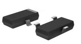 MMBT2907A PNP Transistor: 60V 0.8A, SOT-23 MMBT2907A Bipolar Transistor and Datasheet pdf
20 January 20222087
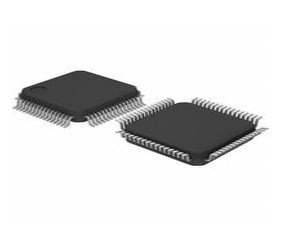 STM32F103RET6 Microcontroller: 72MHz,64-LQFP, Pinout and Features
09 February 20225793
 74HCT14 Hex Inverter: Pinout, Equivalent and Datasheet
20 November 20212567
 STMicroelectronics STM32F051R8T7 Microcontroller Overview: Features and Applications
11 June 2025253
 TIP142 Transistor: Datasheet, Equivalent, Amplifier Circuit
06 December 202113235
 MIC5219 LDO Regulator: Datasheet, Pinout and Circuit
04 August 20214535
 CR2016 Battery: Pinout, Equivalents, CR2016 vs. CR2032
06 October 20213093
 What is TIP3055 Transistor?
25 November 20215725
 How does a Resettable Fuse Work?
26 August 202036308
 What is Spectrum Analyzer?
17 December 20214736
 UTMEL 2024 Annual gala: Igniting Passion, Renewing Brilliance
18 January 20244503
 What is Time Delay Relay?
18 December 202513634
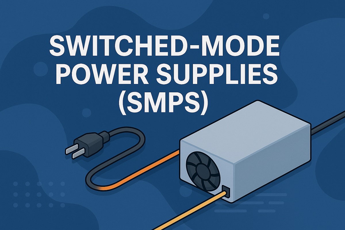 The Impact of SMPS on LED Lighting and Diverse Industries
05 June 20252219
 Shift Register: Classification and Working Principle
26 December 202010691
 Utmel Customer Rating Standard, Rights and Interests
24 July 20203682
 What is LED Drive Power?
18 March 2022750
Texas Instruments
In Stock: 58000
United States
China
Canada
Japan
Russia
Germany
United Kingdom
Singapore
Italy
Hong Kong(China)
Taiwan(China)
France
Korea
Mexico
Netherlands
Malaysia
Austria
Spain
Switzerland
Poland
Thailand
Vietnam
India
United Arab Emirates
Afghanistan
Åland Islands
Albania
Algeria
American Samoa
Andorra
Angola
Anguilla
Antigua & Barbuda
Argentina
Armenia
Aruba
Australia
Azerbaijan
Bahamas
Bahrain
Bangladesh
Barbados
Belarus
Belgium
Belize
Benin
Bermuda
Bhutan
Bolivia
Bonaire, Sint Eustatius and Saba
Bosnia & Herzegovina
Botswana
Brazil
British Indian Ocean Territory
British Virgin Islands
Brunei
Bulgaria
Burkina Faso
Burundi
Cabo Verde
Cambodia
Cameroon
Cayman Islands
Central African Republic
Chad
Chile
Christmas Island
Cocos (Keeling) Islands
Colombia
Comoros
Congo
Congo (DRC)
Cook Islands
Costa Rica
Côte d’Ivoire
Croatia
Cuba
Curaçao
Cyprus
Czechia
Denmark
Djibouti
Dominica
Dominican Republic
Ecuador
Egypt
El Salvador
Equatorial Guinea
Eritrea
Estonia
Eswatini
Ethiopia
Falkland Islands
Faroe Islands
Fiji
Finland
French Guiana
French Polynesia
Gabon
Gambia
Georgia
Ghana
Gibraltar
Greece
Greenland
Grenada
Guadeloupe
Guam
Guatemala
Guernsey
Guinea
Guinea-Bissau
Guyana
Haiti
Honduras
Hungary
Iceland
Indonesia
Iran
Iraq
Ireland
Isle of Man
Israel
Jamaica
Jersey
Jordan
Kazakhstan
Kenya
Kiribati
Kosovo
Kuwait
Kyrgyzstan
Laos
Latvia
Lebanon
Lesotho
Liberia
Libya
Liechtenstein
Lithuania
Luxembourg
Macao(China)
Madagascar
Malawi
Maldives
Mali
Malta
Marshall Islands
Martinique
Mauritania
Mauritius
Mayotte
Micronesia
Moldova
Monaco
Mongolia
Montenegro
Montserrat
Morocco
Mozambique
Myanmar
Namibia
Nauru
Nepal
New Caledonia
New Zealand
Nicaragua
Niger
Nigeria
Niue
Norfolk Island
North Korea
North Macedonia
Northern Mariana Islands
Norway
Oman
Pakistan
Palau
Palestinian Authority
Panama
Papua New Guinea
Paraguay
Peru
Philippines
Pitcairn Islands
Portugal
Puerto Rico
Qatar
Réunion
Romania
Rwanda
Samoa
San Marino
São Tomé & Príncipe
Saudi Arabia
Senegal
Serbia
Seychelles
Sierra Leone
Sint Maarten
Slovakia
Slovenia
Solomon Islands
Somalia
South Africa
South Sudan
Sri Lanka
St Helena, Ascension, Tristan da Cunha
St. Barthélemy
St. Kitts & Nevis
St. Lucia
St. Martin
St. Pierre & Miquelon
St. Vincent & Grenadines
Sudan
Suriname
Svalbard & Jan Mayen
Sweden
Syria
Tajikistan
Tanzania
Timor-Leste
Togo
Tokelau
Tonga
Trinidad & Tobago
Tunisia
Turkey
Turkmenistan
Turks & Caicos Islands
Tuvalu
U.S. Outlying Islands
U.S. Virgin Islands
Uganda
Ukraine
Uruguay
Uzbekistan
Vanuatu
Vatican City
Venezuela
Wallis & Futuna
Yemen
Zambia
Zimbabwe
![SN74ALS139NSR]() SN74ALS139NSR
SN74ALS139NSRTexas Instruments
![SN74CBT3306PWR]() SN74CBT3306PWR
SN74CBT3306PWRTexas Instruments
![SN74CBTS3306PWR]() SN74CBTS3306PWR
SN74CBTS3306PWRTexas Instruments
![SN74LVC157ADBR]() SN74LVC157ADBR
SN74LVC157ADBRTexas Instruments
![SN74LV157APW]() SN74LV157APW
SN74LV157APWTexas Instruments
![SN74CB3Q3306APW]() SN74CB3Q3306APW
SN74CB3Q3306APWTexas Instruments
![SN74HC153N]() SN74HC153N
SN74HC153NTexas Instruments
![SN74AHCT157PW]() SN74AHCT157PW
SN74AHCT157PWTexas Instruments
![SN74CB3T16210DGGR]() SN74CB3T16210DGGR
SN74CB3T16210DGGRTexas Instruments
![SN74CBTLV3245APWR]() SN74CBTLV3245APWR
SN74CBTLV3245APWRTexas Instruments


