
 Product
 Brand
Brand Articles
 Tools
Tools
XC6206 Low ESR Voltage Regulator: Datasheet pdf, Pinout and Equivalents


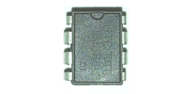
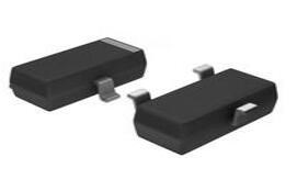
Fixed 0.95mm PMIC 3 TO-236-3, SC-59, SOT-23-3
The XC6206 is a low ESR voltage regulator with a low dropout voltage of 250 mV at 100 mA and low power consumption (1.0 A). This article mainly covers datasheet pdf, pinout, equivalent, circuit, and more details about the XC6206 voltage regulator. Furthermore, there is a huge range of semiconductors, capacitors, resistors, and ICs in stock. Welcome your RFQ!
XC6206 Product Introduction
The XC6206 is a voltage regulator with a low dropout voltage of 250 mV at 100 mA and low power consumption (1.0 A). The XC6206 has a maximum operating voltage of 6.0 V and an output voltage range of 1.2 V to 5 V. This regulator delivers a lot of current with a very low dropout voltage.
XC6206 Pinout

XC6206 Pinout
| Pin No. | Pin Name | Description |
| 1 | VSS | Ground Pin |
| 2 | Vin | Regulated Voltage Input |
| 3 | Vout | Regulated Voltage Output |
XC6206 CAD Model

XC6206 Symbol

XC6206 Footprint
XC6206 Block Diagram

XC6206 Block Diagram
Specifications
- TypeParameter
- Factory Lead Time10 Weeks
- Mount
In electronic components, the term "Mount" typically refers to the method or process of physically attaching or fixing a component onto a circuit board or other electronic device. This can involve soldering, adhesive bonding, or other techniques to secure the component in place. The mounting process is crucial for ensuring proper electrical connections and mechanical stability within the electronic system. Different components may have specific mounting requirements based on their size, shape, and function, and manufacturers provide guidelines for proper mounting procedures to ensure optimal performance and reliability of the electronic device.
Surface Mount - Mounting Type
The "Mounting Type" in electronic components refers to the method used to attach or connect a component to a circuit board or other substrate, such as through-hole, surface-mount, or panel mount.
Surface Mount - Package / Case
refers to the protective housing that encases an electronic component, providing mechanical support, electrical connections, and thermal management.
TO-236-3, SC-59, SOT-23-3 - Usage LevelIndustrial grade
- Operating Temperature
The operating temperature is the range of ambient temperature within which a power supply, or any other electrical equipment, operate in. This ranges from a minimum operating temperature, to a peak or maximum operating temperature, outside which, the power supply may fail.
-40°C~85°C TA - Packaging
Semiconductor package is a carrier / shell used to contain and cover one or more semiconductor components or integrated circuits. The material of the shell can be metal, plastic, glass or ceramic.
Tape & Reel (TR) - Published2011
- JESD-609 Code
The "JESD-609 Code" in electronic components refers to a standardized marking code that indicates the lead-free solder composition and finish of electronic components for compliance with environmental regulations.
e3 - Part Status
Parts can have many statuses as they progress through the configuration, analysis, review, and approval stages.
Active - Moisture Sensitivity Level (MSL)
Moisture Sensitivity Level (MSL) is a standardized rating that indicates the susceptibility of electronic components, particularly semiconductors, to moisture-induced damage during storage and the soldering process, defining the allowable exposure time to ambient conditions before they require special handling or baking to prevent failures
1 (Unlimited) - Number of Terminations3
- ECCN Code
An ECCN (Export Control Classification Number) is an alphanumeric code used by the U.S. Bureau of Industry and Security to identify and categorize electronic components and other dual-use items that may require an export license based on their technical characteristics and potential for military use.
EAR99 - Terminal Finish
Terminal Finish refers to the surface treatment applied to the terminals or leads of electronic components to enhance their performance and longevity. It can improve solderability, corrosion resistance, and overall reliability of the connection in electronic assemblies. Common finishes include nickel, gold, and tin, each possessing distinct properties suitable for various applications. The choice of terminal finish can significantly impact the durability and effectiveness of electronic devices.
Tin (Sn) - Terminal Position
In electronic components, the term "Terminal Position" refers to the physical location of the connection points on the component where external electrical connections can be made. These connection points, known as terminals, are typically used to attach wires, leads, or other components to the main body of the electronic component. The terminal position is important for ensuring proper connectivity and functionality of the component within a circuit. It is often specified in technical datasheets or component specifications to help designers and engineers understand how to properly integrate the component into their circuit designs.
DUAL - Terminal Form
Occurring at or forming the end of a series, succession, or the like; closing; concluding.
GULL WING - Peak Reflow Temperature (Cel)
Peak Reflow Temperature (Cel) is a parameter that specifies the maximum temperature at which an electronic component can be exposed during the reflow soldering process. Reflow soldering is a common method used to attach electronic components to a circuit board. The Peak Reflow Temperature is crucial because it ensures that the component is not damaged or degraded during the soldering process. Exceeding the specified Peak Reflow Temperature can lead to issues such as component failure, reduced performance, or even permanent damage to the component. It is important for manufacturers and assemblers to adhere to the recommended Peak Reflow Temperature to ensure the reliability and functionality of the electronic components.
260 - Number of Functions1
- Terminal Pitch
The center distance from one pole to the next.
0.95mm - Time@Peak Reflow Temperature-Max (s)
Time@Peak Reflow Temperature-Max (s) refers to the maximum duration that an electronic component can be exposed to the peak reflow temperature during the soldering process, which is crucial for ensuring reliable solder joint formation without damaging the component.
10 - Pin Count
a count of all of the component leads (or pins)
3 - JESD-30 Code
JESD-30 Code refers to a standardized descriptive designation system established by JEDEC for semiconductor-device packages. This system provides a systematic method for generating designators that convey essential information about the package's physical characteristics, such as size and shape, which aids in component identification and selection. By using JESD-30 codes, manufacturers and engineers can ensure consistency and clarity in the specification of semiconductor packages across various applications and industries.
R-PDSO-G3 - Voltage - Input (Max)
Voltage - Input (Max) is a parameter in electronic components that specifies the maximum voltage that can be safely applied to the input of the component without causing damage. This parameter is crucial for ensuring the proper functioning and longevity of the component. Exceeding the maximum input voltage can lead to electrical overstress, which may result in permanent damage or failure of the component. It is important to carefully adhere to the specified maximum input voltage to prevent any potential issues and maintain the reliability of the electronic system.
6V - Output Voltage
Output voltage is a crucial parameter in electronic components that refers to the voltage level produced by the component as a result of its operation. It represents the electrical potential difference between the output terminal of the component and a reference point, typically ground. The output voltage is a key factor in determining the performance and functionality of the component, as it dictates the level of voltage that will be delivered to the connected circuit or load. It is often specified in datasheets and technical specifications to ensure compatibility and proper functioning within a given system.
2.5V - Output Type
The "Output Type" parameter in electronic components refers to the type of signal or data that is produced by the component as an output. This parameter specifies the nature of the output signal, such as analog or digital, and can also include details about the voltage levels, current levels, frequency, and other characteristics of the output signal. Understanding the output type of a component is crucial for ensuring compatibility with other components in a circuit or system, as well as for determining how the output signal can be utilized or processed further. In summary, the output type parameter provides essential information about the nature of the signal that is generated by the electronic component as its output.
Fixed - Output Configuration
Output Configuration in electronic components refers to the arrangement or setup of the output pins or terminals of a device. It defines how the output signals are structured and how they interact with external circuits or devices. The output configuration can determine the functionality and compatibility of the component in a circuit design. Common types of output configurations include single-ended, differential, open-drain, and push-pull configurations, each serving different purposes and applications in electronic systems. Understanding the output configuration of a component is crucial for proper integration and operation within a circuit.
Positive - Output Voltage 1
Output Voltage 1 is a parameter commonly found in electronic components such as voltage regulators, power supplies, and amplifiers. It refers to the voltage level that is produced or delivered by the component at a specific output terminal or pin. This parameter is crucial for determining the performance and functionality of the component in a circuit. The specified output voltage should meet the requirements of the connected devices or components to ensure proper operation and compatibility. It is important to carefully consider and verify the output voltage 1 specification when selecting and using electronic components in a design or application.
2.5V - Number of Regulators
A regulator is a mechanism or device that controls something such as pressure, temperature, or fluid flow. The voltage regulator keeps the power level stabilized. A regulator is a mechanism or device that controls something such as pressure, temperature, or fluid flow.
1 - Protection Features
Protection features in electronic components refer to the built-in mechanisms or functionalities designed to safeguard the component and the overall system from various external factors or internal faults. These features are crucial for ensuring the reliability, longevity, and safety of the electronic device. Common protection features include overvoltage protection, overcurrent protection, reverse polarity protection, thermal protection, and short-circuit protection. By activating these features when necessary, the electronic component can prevent damage, malfunctions, or hazards that may arise from abnormal operating conditions or unforeseen events. Overall, protection features play a vital role in enhancing the robustness and resilience of electronic components in diverse applications.
Over Current - Current - Quiescent (Iq)
The parameter "Current - Quiescent (Iq)" in electronic components refers to the amount of current consumed by a device when it is in a quiescent or idle state, meaning when it is not actively performing any tasks or operations. This parameter is important because it represents the baseline power consumption of the device even when it is not actively being used. A lower quiescent current (Iq) value is desirable as it indicates that the device is more energy-efficient and will consume less power when not in use, which can help extend battery life in portable devices and reduce overall power consumption in electronic systems. Designers often pay close attention to the quiescent current specification when selecting components for low-power applications or battery-operated devices.
3μA - Voltage Dropout (Max)
Voltage Dropout (Max) refers to the minimum voltage difference between the input and output of a voltage regulator or linear power supply needed to maintain proper regulation. It indicates the maximum allowable voltage drop across the device for it to function effectively without dropout. If the input voltage falls below this threshold, the output voltage may drop below the specified level, leading to potential operational issues for connected components. This parameter is critical for ensuring stable and reliable power delivery in electronic circuits.
0.71V @ 100mA - Dropout Voltage
Dropout voltage is the input-to-output differential voltage at which the circuit ceases to regulate against further reductions in input voltage; this point occurs when the input voltage approaches the output voltage.
350mV - Length2.9mm
- RoHS Status
RoHS means “Restriction of Certain Hazardous Substances” in the “Hazardous Substances Directive” in electrical and electronic equipment.
ROHS3 Compliant
XC6206 Features
Output Voltage Range 1.2V to 5.0V (selectable in 100mV steps)
Highly Accurate ± 2%
Dropout Voltage 160mV @ 50mA (3.0V type)
Low Power Consumption 2μA (TYP)
Maximum Output Current 100mA (Vin≥Vout+1V)
Internal protector current limiter and short protector
Small packages SOT-89-3, SOT-23-3, SOT23-3B, SOT353, and other required
XC6206 Applications
Smartphones / Mobile phones
Portable game consoles
Digital still cameras / Camcorders
Digital audio equipment
Reference voltage sources
Multi-function power supplies
XC6206 Equivalents
XC6206 Equivalents for XC6216
How to Use XC6206
The XC6206 is easy to use because just three pins need to be connected. A 1 f ceramic capacitor connects the VIN pin of the XC6206 to the input supply voltage. To decrease input noise, a ceramic capacitor is utilized. The VSS pin is connected to the ground, while the Vout pin provides a regulated output. The XC6206 application circuit is shown below.


XC6206 Application Circuit
Parts with Similar Specs
- ImagePart NumberManufacturerPackage / CaseVoltage - Input (Max)Output VoltageDropout VoltageTechnologyTerminal PitchOutput TypeFactory Lead TimeView Compare
![XC6206P252MR-G]()
XC6206P252MR-G
TO-236-3, SC-59, SOT-23-3
6V
2.5 V
350 mV
CMOS
0.95 mm
Fixed
10 Weeks
![MCP1701AT-5002I/CB]()
TO-236-3, SC-59, SOT-23-3
10V
5 V
380 mV
CMOS
0.95 mm
Fixed
10 Weeks


XC6206 Package Dimensions

XC6206 Package Dimensions
XC6206 Manufacturer
Torex has grown rapidly as a leading manufacturer of CMOS power management ICs which are widely used for energy-efficient applications powered by batteries. They provide the main supply line of voltage regulators, voltage detectors, and DC/DC converters. They also provide high-quality products including charge pump ICs, Multi-Chip Modules, Mosfets, op-amps, oscillators, etc. Based on their unique tenet of "Green Operation", Torex designs and develops CMOS analog technologies combined with their high-performance products to meet the specific requirements of their customers. Their devices can switch between two modes: high speed and power save automatically or manually, which depends on the load current.
Trend Analysis
Datasheet PDF
- Datasheets :
- Environmental Information :
What is the function of XC6206?
An XC6206 is to regulate a voltage by turning excess power into heat, making this integrated circuit a good fit for low-power or small VIN-to-VOUT differential applications.
How does XC6206 calculate dropout voltage?
Dropout is defined as the input voltage minus the output voltage at this point. If VIN = 3.5 V when VOUT = 3.2 V, the LDO has a 300-mV dropout voltage.
What is the voltage of XC6206?
XC6206 is a highly precise voltage regulator with low power consumption (1.0 µA) and a low dropout voltage of 250 mV at 100 mA. The maximum operating voltage for XC6206 is 6.0 V and the output voltage range is 1.2 V to 5 V.
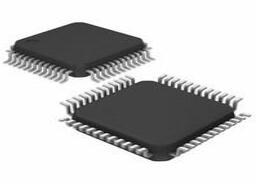 KSZ8863RLLI IC ETHERNET SWITCH 3PORT 48-LQFP: Datasheet, Pinout, and Applications
01 March 20221463
![How to Use 2N3819? [Video]](https://res.utmel.com/Images/Article/a64515f9-a471-49f9-b346-a5fe0f422e73.jpg) How to Use 2N3819? [Video]
How to Use 2N3819? [Video]23 September 20221683
 STM32L010F4P6: Features, Applications, and Datasheet
29 November 20231910
 Audio Amplifier IC LM386:Where/How to use?
05 May 202211755
 AO3400 30V N-Channel MOSFET, 5.8A SOT23-3 and AO3400 Pinout
28 January 202216182
 L297 Stepper Motor Driver Controller: Datasheet, L297 and L298
23 November 20217816
 STM32F401VDH6 Microcontroller: Pinout, Datasheet, Features
29 July 20214179
 Yageo RC0603JR-070RL Alternatives: Best 0603 Zero Ohm Resistor Replacements
08 September 20251080
 Shenzhen: This Year Will Focus on Promoting SMIC and CR Micro 12-inch Project
13 April 20226885
 What is a Switched Reluctance Motor?
09 July 20248582
 Introduction to AC motor
05 March 20219375
 Filters Explained: Principles, Parameters and Application Guide
09 April 202512239
 What is a High-pass Filter?
10 March 202114646
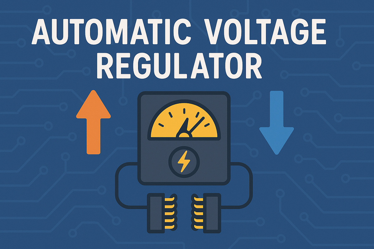 Automatic Voltage Regulator: Ultimate Guide to Stable Power and Equipment Protection
06 May 20259567
 Three Phase Inverter - 180 Degree Conduction Mode
05 October 202320583
![How a CPU is made? [HD Graphics]](https://res.utmel.com/Images/Article/d7470283-3897-4776-abd1-e7eef60aff17.jpg) How a CPU is made? [HD Graphics]
How a CPU is made? [HD Graphics]07 January 202617096
Torex Semiconductor Ltd
In Stock: 60000
Minimum: 1 Multiples: 1
Qty
Unit Price
Ext Price
1
$0.479012
$0.48
10
$0.451898
$4.52
100
$0.426319
$42.63
500
$0.402188
$201.09
1000
$0.379422
$379.42
Not the price you want? Send RFQ Now and we'll contact you ASAP.
Inquire for More Quantity
![XC6221A332MR-G]() XC6221A332MR-G
XC6221A332MR-GTorex Semiconductor Ltd
![XC6220B331MR-G]() XC6220B331MR-G
XC6220B331MR-GTorex Semiconductor Ltd
![XC6210B332MR-G]() XC6210B332MR-G
XC6210B332MR-GTorex Semiconductor Ltd
![XC6206P332MR-G]() XC6206P332MR-G
XC6206P332MR-GTorex Semiconductor Ltd
![XC6204B502MR-G]() XC6204B502MR-G
XC6204B502MR-GTorex Semiconductor Ltd
![XC6222B331MR-G]() XC6222B331MR-G
XC6222B331MR-GTorex Semiconductor Ltd
![XC6221B332MR-G]() XC6221B332MR-G
XC6221B332MR-GTorex Semiconductor Ltd
![XC6220B281PR-G]() XC6220B281PR-G
XC6220B281PR-GTorex Semiconductor Ltd
![XC6227C331MR-G]() XC6227C331MR-G
XC6227C331MR-GTorex Semiconductor Ltd
![XC6220B331PR-G]() XC6220B331PR-G
XC6220B331PR-GTorex Semiconductor Ltd


