

 Product
 Brand
Brand Articles
 Tools
Tools
AD9520-0BCPZ Clock Generators: Pinout, Feature, Specification

3.3V Clock Generator, Fanout Distribution AD9520 Clock Generators 64 Pins 64-VFQFN Exposed Pad, CSP 64 Terminals Surface Mount 3.135V~3.465V Tray


3.3V Clock Generator, Fanout Distribution AD9520 Clock Generators 64 Pins 64-VFQFN Exposed Pad, CSP 64 Terminals Surface Mount 3.135V~3.465V Tray
The AD9520-0BCPZ is IC CLOCK GEN 2.8GHZ VCO 64LFCSP, which is designed to work as Clock/Timing - Clock Generators, PLLs, Frequency Synthesizers.
AD9520-0BCPZ Pinout
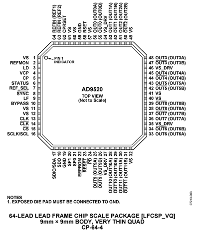
AD9520-0BCPZ Feature
Low phase noise, phase-locked loop (PLL)
On-chip VCO tunes from 2.53 GHz to 2.95 GHz Optional external 3.3 V/5 V VCO/VCXO to 2.4 GHz 1 differential or 2 single-ended reference inputs
Accepts CMOS, LVDS, or LVPECL references to 250 MHz Accepts 16.62 MHz to 33.3 MHz crystal for reference input
Optional reference clock doubler
Reference monitoring capability
Automatic/manual reference holdover and reference switchover modes, with revertive switching Glitch-free switchover between references
Automatic recovery from holdover
Digital or analog lock detect, selectable
Optional zero delay operation
Twelve 1.6 GHz LVPECL outputs divided into 4 groups
Each group of 3 outputs shares a 1-to-32 divider with phase delay
Additive output jitter as low as 225 fs rms
Channel-to-channel skew grouped outputs < 16 ps
Each LVPECL output can be configured as 2 CMOS outputs (for fOUT ≤ 250 MHz)
Automatic synchronization of all outputs on power-up
Manual output synchronization available
SPI- and I²C-compatible serial control port
64-lead LFCSP
Nonvolatile EEPROM stores configuration settings
AD9520-0BCPZ Advantage
The AD9520-0BCPZ provides a multi-output clock distribution function with subpicosecond jitter performance, along with an on-chip PLL and VCO. The on-chip VCO tunes from 2.53 GHz to 2.95 GHz. An external 3.3 V/5 V VCO/VCXO of up to 2.4 GHz can also be used.
The AD9520-0BCPZ serial interface supports both SPI and I²C ports. An in-package EEPROM, which can be programmed through the serial interface, can store user-defined register settings for power-up and chip reset.
The AD9520-0BCPZ features 12 LVPECL outputs in four groups. Any of the 1.6 GHz LVPECL outputs can be reconfigured as two 250 MHz CMOS outputs. If an application requires LVDS drivers instead of LVPECL drivers, refer to the AD9520-0BCPZ.
Each group of three outputs has a divider that allows both the divide ratio (from 1 to 32) and the phase offset or coarse time delay to be set.
The AD9520-0BCPZ is available in a 64-lead LFCSP and can be operated from a single 3.3 V supply. The external VCO can have an operating voltage of up to 5.5 V. A separate output driver power supply can be from 2.375 V to 3.465 V.
The AD9520-0BCPZ is specified for operation over the standard industrial range of −40°C to +85°C.
Specifications
- TypeParameter
- Lifecycle Status
Lifecycle Status refers to the current stage of an electronic component in its product life cycle, indicating whether it is active, obsolete, or transitioning between these states. An active status means the component is in production and available for purchase. An obsolete status indicates that the component is no longer being manufactured or supported, and manufacturers typically provide a limited time frame for support. Understanding the lifecycle status is crucial for design engineers to ensure continuity and reliability in their projects.
PRODUCTION (Last Updated: 3 weeks ago) - Factory Lead Time8 Weeks
- Mounting Type
The "Mounting Type" in electronic components refers to the method used to attach or connect a component to a circuit board or other substrate, such as through-hole, surface-mount, or panel mount.
Surface Mount - Package / Case
refers to the protective housing that encases an electronic component, providing mechanical support, electrical connections, and thermal management.
64-VFQFN Exposed Pad, CSP - Surface Mount
having leads that are designed to be soldered on the side of a circuit board that the body of the component is mounted on.
YES - Number of Pins64
- Frequency(Max)2.95GHz
- Operating Temperature
The operating temperature is the range of ambient temperature within which a power supply, or any other electrical equipment, operate in. This ranges from a minimum operating temperature, to a peak or maximum operating temperature, outside which, the power supply may fail.
-40°C~85°C - Packaging
Semiconductor package is a carrier / shell used to contain and cover one or more semiconductor components or integrated circuits. The material of the shell can be metal, plastic, glass or ceramic.
Tray - JESD-609 Code
The "JESD-609 Code" in electronic components refers to a standardized marking code that indicates the lead-free solder composition and finish of electronic components for compliance with environmental regulations.
e3 - Pbfree Code
The "Pbfree Code" parameter in electronic components refers to the code or marking used to indicate that the component is lead-free. Lead (Pb) is a toxic substance that has been widely used in electronic components for many years, but due to environmental concerns, there has been a shift towards lead-free alternatives. The Pbfree Code helps manufacturers and users easily identify components that do not contain lead, ensuring compliance with regulations and promoting environmentally friendly practices. It is important to pay attention to the Pbfree Code when selecting electronic components to ensure they meet the necessary requirements for lead-free applications.
no - Part Status
Parts can have many statuses as they progress through the configuration, analysis, review, and approval stages.
Active - Moisture Sensitivity Level (MSL)
Moisture Sensitivity Level (MSL) is a standardized rating that indicates the susceptibility of electronic components, particularly semiconductors, to moisture-induced damage during storage and the soldering process, defining the allowable exposure time to ambient conditions before they require special handling or baking to prevent failures
3 (168 Hours) - Number of Terminations64
- ECCN Code
An ECCN (Export Control Classification Number) is an alphanumeric code used by the U.S. Bureau of Industry and Security to identify and categorize electronic components and other dual-use items that may require an export license based on their technical characteristics and potential for military use.
EAR99 - TypeClock Generator, Fanout Distribution
- Terminal Finish
Terminal Finish refers to the surface treatment applied to the terminals or leads of electronic components to enhance their performance and longevity. It can improve solderability, corrosion resistance, and overall reliability of the connection in electronic assemblies. Common finishes include nickel, gold, and tin, each possessing distinct properties suitable for various applications. The choice of terminal finish can significantly impact the durability and effectiveness of electronic devices.
Tin (Sn) - Voltage - Supply
Voltage - Supply refers to the range of voltage levels that an electronic component or circuit is designed to operate with. It indicates the minimum and maximum supply voltage that can be applied for the device to function properly. Providing supply voltages outside this range can lead to malfunction, damage, or reduced performance. This parameter is critical for ensuring compatibility between different components in a circuit.
3.135V~3.465V - Terminal Position
In electronic components, the term "Terminal Position" refers to the physical location of the connection points on the component where external electrical connections can be made. These connection points, known as terminals, are typically used to attach wires, leads, or other components to the main body of the electronic component. The terminal position is important for ensuring proper connectivity and functionality of the component within a circuit. It is often specified in technical datasheets or component specifications to help designers and engineers understand how to properly integrate the component into their circuit designs.
QUAD - Terminal Form
Occurring at or forming the end of a series, succession, or the like; closing; concluding.
NO LEAD - Peak Reflow Temperature (Cel)
Peak Reflow Temperature (Cel) is a parameter that specifies the maximum temperature at which an electronic component can be exposed during the reflow soldering process. Reflow soldering is a common method used to attach electronic components to a circuit board. The Peak Reflow Temperature is crucial because it ensures that the component is not damaged or degraded during the soldering process. Exceeding the specified Peak Reflow Temperature can lead to issues such as component failure, reduced performance, or even permanent damage to the component. It is important for manufacturers and assemblers to adhere to the recommended Peak Reflow Temperature to ensure the reliability and functionality of the electronic components.
260 - Supply Voltage
Supply voltage refers to the electrical potential difference provided to an electronic component or circuit. It is crucial for the proper operation of devices, as it powers their functions and determines performance characteristics. The supply voltage must be within specified limits to ensure reliability and prevent damage to components. Different electronic devices have specific supply voltage requirements, which can vary widely depending on their design and intended application.
3.3V - Terminal Pitch
The center distance from one pole to the next.
0.5mm - Frequency
In electronic components, the parameter "Frequency" refers to the rate at which a signal oscillates or cycles within a given period of time. It is typically measured in Hertz (Hz) and represents how many times a signal completes a full cycle in one second. Frequency is a crucial aspect in electronic components as it determines the behavior and performance of various devices such as oscillators, filters, and communication systems. Understanding the frequency characteristics of components is essential for designing and analyzing electronic circuits to ensure proper functionality and compatibility with other components in a system.
1.6GHz - Time@Peak Reflow Temperature-Max (s)
Time@Peak Reflow Temperature-Max (s) refers to the maximum duration that an electronic component can be exposed to the peak reflow temperature during the soldering process, which is crucial for ensuring reliable solder joint formation without damaging the component.
30 - Base Part Number
The "Base Part Number" (BPN) in electronic components serves a similar purpose to the "Base Product Number." It refers to the primary identifier for a component that captures the essential characteristics shared by a group of similar components. The BPN provides a fundamental way to reference a family or series of components without specifying all the variations and specific details.
AD9520 - Output
In electronic components, the parameter "Output" typically refers to the signal or data that is produced by the component and sent to another part of the circuit or system. The output can be in the form of voltage, current, frequency, or any other measurable quantity depending on the specific component. The output of a component is often crucial in determining its functionality and how it interacts with other components in the circuit. Understanding the output characteristics of electronic components is essential for designing and troubleshooting electronic circuits effectively.
CMOS, LVPECL - Pin Count
a count of all of the component leads (or pins)
64 - Number of Outputs12
- Qualification Status
An indicator of formal certification of qualifications.
Not Qualified - Operating Supply Voltage
The voltage level by which an electrical system is designated and to which certain operating characteristics of the system are related.
3.3V - Number of Circuits1
- Logic Function
In electronic components, the term "Logic Function" refers to the specific operation or behavior of a component based on its input signals. It describes how the component processes the input signals to produce the desired output. Logic functions are fundamental to digital circuits and are used to perform logical operations such as AND, OR, NOT, and XOR.Each electronic component, such as logic gates or flip-flops, is designed to perform a specific logic function based on its internal circuitry. By understanding the logic function of a component, engineers can design and analyze complex digital systems to ensure proper functionality and performance. Different logic functions can be combined to create more complex operations, allowing for the creation of sophisticated digital devices and systems.
Clock - Input
In electronic components, "Input" refers to the signal or data that is provided to a device or system for processing or manipulation. It is the information or command that is received by the component to initiate a specific function or operation. The input can come from various sources such as sensors, other electronic devices, or user interactions. It is crucial for the proper functioning of the component as it determines how the device will respond or behave based on the input received. Understanding and managing the input parameters is essential in designing and using electronic components effectively.
CMOS, LVDS, LVPECL - Ratio - Input:Output
The parameter "Ratio - Input:Output" in electronic components refers to the relationship between the input and output quantities of a device or system. It is a measure of how the input signal or energy is transformed or converted into the output signal or energy. This ratio is often expressed as a numerical value or percentage, indicating the efficiency or effectiveness of the component in converting the input to the desired output. A higher ratio typically signifies better performance or higher efficiency, while a lower ratio may indicate losses or inefficiencies in the conversion process. Understanding and optimizing the input-output ratio is crucial in designing and evaluating electronic components for various applications.
2:12, 2:24 - Primary Clock/Crystal Frequency-Nom
The parameter "Primary Clock/Crystal Frequency-Nom" refers to the nominal frequency at which a clock or crystal oscillator operates in electronic components. This frequency is critical for synchronizing the timing of various processes within a circuit or system. It is typically specified in hertz and indicates the standard or average frequency that the oscillator is designed to achieve under normal operating conditions. Accurate frequency is essential for ensuring proper functioning and performance of digital circuits and communication systems.
33.33MHz - PLL
PLL stands for Phase-Locked Loop, which is a control system that generates an output signal whose phase is related to the phase of an input signal. It is commonly used in electronic components to synchronize, modulate, demodulate, filter, or recover a signal's frequency. A PLL typically consists of a phase detector, a loop filter, a voltage-controlled oscillator (VCO), and a feedback circuit. The PLL locks the phase of the output signal to the phase of the input signal, making it a versatile tool in various applications such as frequency synthesis, clock recovery, and frequency modulation.
Yes - Differential - Input:Output
Differential - Input:Output refers to the relationship between the input and output signals in differential amplifiers or circuits. It measures the difference in voltage between two input terminals and produces an output that is proportional to this difference. This parameter is essential for noise rejection and improving signal integrity in various applications, such as operational amplifiers and data acquisition systems. It allows circuits to effectively amplify small signals while minimizing interference and common-mode noise.
Yes/Yes - Max Duty Cycle
Max Duty Cycle refers to the maximum percentage of time that an electronic component, such as a switch or a power supply, can be in an "on" state during a defined time period. It is an important parameter in pulse-width modulated (PWM) systems and helps determine how often a device can operate without overheating or sustaining damage. By specifying the maximum duty cycle, manufacturers provide guidance on the safe operational limits of the component, ensuring reliability and efficiency in various applications.
50 % - Divider/Multiplier
The parameter "Divider/Multiplier" in electronic components refers to a feature that allows the component to divide or multiply an input signal by a certain factor. This feature is commonly found in components such as operational amplifiers, voltage regulators, and signal processing circuits. In the context of operational amplifiers, the Divider/Multiplier parameter indicates the ability of the amplifier to scale the input signal by a specific factor, either dividing it or multiplying it. This can be useful for adjusting the amplitude or gain of a signal in a circuit.Overall, the Divider/Multiplier parameter provides flexibility in signal processing applications by allowing users to manipulate the input signal according to their specific requirements, whether it involves scaling down the signal for further processing or amplifying it for increased output.
Yes/No - Height950μm
- Length9.1mm
- Width9.1mm
- REACH SVHC
The parameter "REACH SVHC" in electronic components refers to the compliance with the Registration, Evaluation, Authorization, and Restriction of Chemicals (REACH) regulation regarding Substances of Very High Concern (SVHC). SVHCs are substances that may have serious effects on human health or the environment, and their use is regulated under REACH to ensure their safe handling and minimize their impact.Manufacturers of electronic components need to declare if their products contain any SVHCs above a certain threshold concentration and provide information on the safe use of these substances. This information allows customers to make informed decisions about the potential risks associated with using the components and take appropriate measures to mitigate any hazards.Ensuring compliance with REACH SVHC requirements is essential for electronics manufacturers to meet regulatory standards, protect human health and the environment, and maintain transparency in their supply chain. It also demonstrates a commitment to sustainability and responsible manufacturing practices in the electronics industry.
No SVHC - RoHS Status
RoHS means “Restriction of Certain Hazardous Substances” in the “Hazardous Substances Directive” in electrical and electronic equipment.
ROHS3 Compliant - Lead Free
Lead Free is a term used to describe electronic components that do not contain lead as part of their composition. Lead is a toxic material that can have harmful effects on human health and the environment, so the electronics industry has been moving towards lead-free components to reduce these risks. Lead-free components are typically made using alternative materials such as silver, copper, and tin. Manufacturers must comply with regulations such as the Restriction of Hazardous Substances (RoHS) directive to ensure that their products are lead-free and environmentally friendly.
Contains Lead
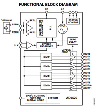
AD9520-0BCPZ Functional Block Diagram
AD9520-0BCPZ Application
Low jitter, low phase noise clock distribution
Clock generation and translation for SONET, 10Ge, 10GFC, Synchronous Ethernet, OTU2/3/4 Forward error correction (G.710)
Clocking high-speed ADCs, DACs, DDSs, DDCs, DUCs, MxFEs
High-performance wireless transceivers
ATE and high-performance instrumentation
Broadband infrastructures
Parts with Similar Specs
- ImagePart NumberManufacturerPackage / CaseNumber of PinsPLLInputFrequency (Max)Number of OutputsSupply VoltageTerminal PitchView Compare
![AD9520-0BCPZ]()
AD9520-0BCPZ
64-VFQFN Exposed Pad, CSP
64
Yes
CMOS, LVDS, LVPECL
2.95GHz
12
3.3 V
0.5 mm
![AD9517-0ABCPZ]()
64-VFQFN Exposed Pad, CSP
64
Yes
CMOS, LVDS, LVPECL
-
12
3.3 V
0.5 mm
![AD9522-0BCPZ]()
64-VFQFN Exposed Pad, CSP
64
Yes
CMOS, LVDS, LVPECL
-
12
3.3 V
0.5 mm
![AD9522-5BCPZ]()
48-VFQFN Exposed Pad, CSP
48
Yes
CMOS, LVDS, LVPECL
-
12
3.3 V
0.5 mm


AD9520-0BCPZ Manufacture
Analog Devices (NASDAQ: ADI) is a world leader in the design, manufacture, and marketing of a broad portfolio of high performance analog, mixed-signal, and digital signal processing (DSP) integrated circuits (ICs) used in virtually all types of electronic equipment. Since our inception in 1965, we have focused on solving the engineering challenges associated with signal processing in electronic equipment. Used by over 100,000 customers worldwide, our signal processing products play a fundamental role in converting, conditioning, and processing real-world phenomena such as temperature, pressure, sound, light, speed, and motion into electrical signals to be used in a wide array of electronic devices.
Trend Analysis
Datasheet PDF
- Datasheets :
- Design Resources :
- PCN Design/Specification :
- ConflictMineralStatement :
1.What happens if I run the part in an ambient environment which exceeds 85°C?
ADI does not guarantee specs on parts operating outside the temperature range listed in the product datasheet. The user may find that devices operate outside rated temperatures, but ADI does not recommend exceeding datasheet limits.
2.What is the difference between the coarse phase adjust and the fine delay adjust?
On the AD951x clock ICs, each output has a divider which features a coarse phase (or delay) adjust which allows for the selection of a given clock edge within the divide period as a delay or phase offset for that output. This feature adds no jitter to the clock output, but only allows for discrete delays in steps the size of the input clock period. However, certain outputs also have a feature called a fine delay adjust. This feature is only available on certain LVDS/CMOS outputs, and never on an LVPECL output.
3.What is the effect of distributing harmonically related clocks (on chip or on board) in terms of jitter?
Harmonically related clocks in general do not produce extra jitter. However, the variation in propagation times can cause edges to occur noncoincidentally. This can possibly produce jitter if the amplitudes of the various edges are too high at a given node.
4.May I use the AD9540 for spread spectrum clocking?
The AD9540 is capable of doing a frequency sweep function which can be used for the EMI reduction technique called Spread Spectrum Clock Generation. A triangular waveform is easy to achieve using the frequency accumulator available on that product. Non-triangular waveforms can also be constructed using the profile registers to drive changes to the "Delta Frequency Tuning" word which is used by the frequency accumulator.
5.My application has pretty tight power consumption requirements. I am very interested in the capabilities of the AD9510, but I don't need every feature. Is it possible to turn off the unused features and save power?
Yes. It is very possible to turn off unused sections of the AD951x chips. There is a high degree of configuration which allows unused inputs, outputs, and the PLL to be powered off when not needed or not used. The programming register table shows the bits which control these power downs.
 2SA1302 PNP Transistor, 15A, 200V, TO-3PL Silicon Transistor, 2SA1302 Pinout
29 December 20213223
 IR2153 Half-Bridge Driver: Datasheet, Circuit and Equivalent
14 October 202116107
 SS14 Diode: Package, Pinout and Datasheet
24 August 20219181
 ISL80103IRAJZ Linear Regulator: Diagram, Pinout, and Datasheet
28 February 2022794
 DS3232 RTC: Pinout, Datasheet and DS3232 vs. DS3231
28 March 20245798
 1N4148W-7-F Switching Diode: Features, Pinout, and Datasheet
23 April 2022701
 L7805ACV Voltage Regulator: Pinout, Applications and Datasheet
21 November 20231607
 What’s the relationship between CR1616 and CR1632?
31 May 202230854
 Varistor: Definition, Function, Working and Testing
03 April 202584538
 H-bridge: Working, Circuits and Applications
03 December 202146479
 What is a PIN Diode?
04 February 202110280
 What is 3D Printing Technology (3DP)?
18 January 20224255
 How to Choose the Right Spade Connector for Any Project
18 July 20259910
 Advanced Wide-Bandgap Semiconductor Ultraviolet Photodetectors for Enhanced Detection and Imaging
04 December 20231964
 What Makes Rocker Switches Unique
18 July 20251291
 Coping with Radiation-Induced Deterioration in Wide and UltraWide Bandgap Semiconductors
01 December 20232120
Analog Devices Inc.
In Stock
United States
China
Canada
Japan
Russia
Germany
United Kingdom
Singapore
Italy
Hong Kong(China)
Taiwan(China)
France
Korea
Mexico
Netherlands
Malaysia
Austria
Spain
Switzerland
Poland
Thailand
Vietnam
India
United Arab Emirates
Afghanistan
Åland Islands
Albania
Algeria
American Samoa
Andorra
Angola
Anguilla
Antigua & Barbuda
Argentina
Armenia
Aruba
Australia
Azerbaijan
Bahamas
Bahrain
Bangladesh
Barbados
Belarus
Belgium
Belize
Benin
Bermuda
Bhutan
Bolivia
Bonaire, Sint Eustatius and Saba
Bosnia & Herzegovina
Botswana
Brazil
British Indian Ocean Territory
British Virgin Islands
Brunei
Bulgaria
Burkina Faso
Burundi
Cabo Verde
Cambodia
Cameroon
Cayman Islands
Central African Republic
Chad
Chile
Christmas Island
Cocos (Keeling) Islands
Colombia
Comoros
Congo
Congo (DRC)
Cook Islands
Costa Rica
Côte d’Ivoire
Croatia
Cuba
Curaçao
Cyprus
Czechia
Denmark
Djibouti
Dominica
Dominican Republic
Ecuador
Egypt
El Salvador
Equatorial Guinea
Eritrea
Estonia
Eswatini
Ethiopia
Falkland Islands
Faroe Islands
Fiji
Finland
French Guiana
French Polynesia
Gabon
Gambia
Georgia
Ghana
Gibraltar
Greece
Greenland
Grenada
Guadeloupe
Guam
Guatemala
Guernsey
Guinea
Guinea-Bissau
Guyana
Haiti
Honduras
Hungary
Iceland
Indonesia
Iran
Iraq
Ireland
Isle of Man
Israel
Jamaica
Jersey
Jordan
Kazakhstan
Kenya
Kiribati
Kosovo
Kuwait
Kyrgyzstan
Laos
Latvia
Lebanon
Lesotho
Liberia
Libya
Liechtenstein
Lithuania
Luxembourg
Macao(China)
Madagascar
Malawi
Maldives
Mali
Malta
Marshall Islands
Martinique
Mauritania
Mauritius
Mayotte
Micronesia
Moldova
Monaco
Mongolia
Montenegro
Montserrat
Morocco
Mozambique
Myanmar
Namibia
Nauru
Nepal
New Caledonia
New Zealand
Nicaragua
Niger
Nigeria
Niue
Norfolk Island
North Korea
North Macedonia
Northern Mariana Islands
Norway
Oman
Pakistan
Palau
Palestinian Authority
Panama
Papua New Guinea
Paraguay
Peru
Philippines
Pitcairn Islands
Portugal
Puerto Rico
Qatar
Réunion
Romania
Rwanda
Samoa
San Marino
São Tomé & Príncipe
Saudi Arabia
Senegal
Serbia
Seychelles
Sierra Leone
Sint Maarten
Slovakia
Slovenia
Solomon Islands
Somalia
South Africa
South Sudan
Sri Lanka
St Helena, Ascension, Tristan da Cunha
St. Barthélemy
St. Kitts & Nevis
St. Lucia
St. Martin
St. Pierre & Miquelon
St. Vincent & Grenadines
Sudan
Suriname
Svalbard & Jan Mayen
Sweden
Syria
Tajikistan
Tanzania
Timor-Leste
Togo
Tokelau
Tonga
Trinidad & Tobago
Tunisia
Turkey
Turkmenistan
Turks & Caicos Islands
Tuvalu
U.S. Outlying Islands
U.S. Virgin Islands
Uganda
Ukraine
Uruguay
Uzbekistan
Vanuatu
Vatican City
Venezuela
Wallis & Futuna
Yemen
Zambia
Zimbabwe
![ADF4118BRU-REEL7]() ADF4118BRU-REEL7
ADF4118BRU-REEL7Analog Devices Inc.
![AD9522-3BCPZ]() AD9522-3BCPZ
AD9522-3BCPZAnalog Devices Inc.
![AD9518-4ABCPZ]() AD9518-4ABCPZ
AD9518-4ABCPZAnalog Devices Inc.
![AD9517-3ABCPZ]() AD9517-3ABCPZ
AD9517-3ABCPZAnalog Devices Inc.
![AD9542BCPZ-REEL7]() AD9542BCPZ-REEL7
AD9542BCPZ-REEL7Analog Devices Inc.
![AD9574BCPZ]() AD9574BCPZ
AD9574BCPZAnalog Devices Inc.
![ADF4110BCPZ]() ADF4110BCPZ
ADF4110BCPZAnalog Devices Inc.
![ADF4113HVBRUZ]() ADF4113HVBRUZ
ADF4113HVBRUZAnalog Devices Inc.
![ADF4150HVBCPZ]() ADF4150HVBCPZ
ADF4150HVBCPZAnalog Devices Inc.


