
2N3055 NPN Power Transistor: Datasheet, Pinout and Specifications

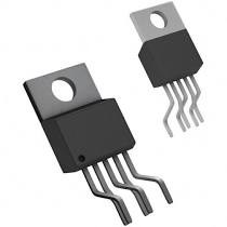
STMICROELECTRONICS 2N3055 Bipolar (BJT) Single Transistor, NPN, 60 V, 3 MHz, 115 W, 15 A, 70 hFE


STMICROELECTRONICS 2N3055 Bipolar (BJT) Single Transistor, NPN, 60 V, 3 MHz, 115 W, 15 A, 70 hFE
2N3055 is a complementary silicon power transistor. This article mainly introduces pinout, specifications, features, and other detailed information about STMicroelectronics 2N3055.

2N3055 Power Transistor Test
2N3055 Description
The 2N3055 is a silicon Epitaxial-Base Planar NPN transistor mounted in Jedec TO-3 metal case. It is intended for power switching circuits, series and shunt regulators, output stages, and high fidelity amplifiers. The complementary PNP type is MJ2955.
2N3055 Pinout


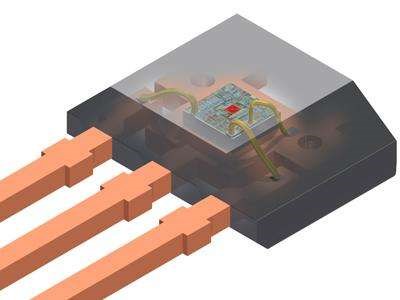
2N3055 CAD model

2N3055 symbol

2N3055 footprint

2N3055 3D model
2N3055 Features
Medium power transistor
Excellent safe operating area
Complementary NPN - PNP transistors
Low collector-emitter saturation voltage
Pb−free packages are available
DC current gain (hFE) up to 70
With hfe improved linearity
Maximum voltage across collector and emitter: 60V DC
Maximum current allowed trough collector: 15A DC
Maximum voltage across base and emitter: 7V DC
Maximum current allowed through base: 7A DC
Maximum voltage across collector and base: 100V DC
Operating temperature range: -65ºC to +200ºC
Total power dissipation: 115W
Parts with Similar Specs
Specifications
- TypeParameter
- Mount
In electronic components, the term "Mount" typically refers to the method or process of physically attaching or fixing a component onto a circuit board or other electronic device. This can involve soldering, adhesive bonding, or other techniques to secure the component in place. The mounting process is crucial for ensuring proper electrical connections and mechanical stability within the electronic system. Different components may have specific mounting requirements based on their size, shape, and function, and manufacturers provide guidelines for proper mounting procedures to ensure optimal performance and reliability of the electronic device.
Chassis Mount, Through Hole - Mounting Type
The "Mounting Type" in electronic components refers to the method used to attach or connect a component to a circuit board or other substrate, such as through-hole, surface-mount, or panel mount.
Chassis Mount - Package / Case
refers to the protective housing that encases an electronic component, providing mechanical support, electrical connections, and thermal management.
TO-204AA, TO-3 - Number of Pins2
- Weight4.535924g
- Transistor Element Material
The "Transistor Element Material" parameter in electronic components refers to the material used to construct the transistor within the component. Transistors are semiconductor devices that amplify or switch electronic signals and are a fundamental building block in electronic circuits. The material used for the transistor element can significantly impact the performance and characteristics of the component. Common materials used for transistor elements include silicon, germanium, and gallium arsenide, each with its own unique properties and suitability for different applications. The choice of transistor element material is crucial in designing electronic components to meet specific performance requirements such as speed, power efficiency, and temperature tolerance.
SILICON - Collector-Emitter Breakdown Voltage60V
- Collector-Emitter Saturation Voltage1V
- Number of Elements1
- hFEMin20
- Operating Temperature
The operating temperature is the range of ambient temperature within which a power supply, or any other electrical equipment, operate in. This ranges from a minimum operating temperature, to a peak or maximum operating temperature, outside which, the power supply may fail.
200°C TJ - Packaging
Semiconductor package is a carrier / shell used to contain and cover one or more semiconductor components or integrated circuits. The material of the shell can be metal, plastic, glass or ceramic.
Tray - JESD-609 Code
The "JESD-609 Code" in electronic components refers to a standardized marking code that indicates the lead-free solder composition and finish of electronic components for compliance with environmental regulations.
e3 - Pbfree Code
The "Pbfree Code" parameter in electronic components refers to the code or marking used to indicate that the component is lead-free. Lead (Pb) is a toxic substance that has been widely used in electronic components for many years, but due to environmental concerns, there has been a shift towards lead-free alternatives. The Pbfree Code helps manufacturers and users easily identify components that do not contain lead, ensuring compliance with regulations and promoting environmentally friendly practices. It is important to pay attention to the Pbfree Code when selecting electronic components to ensure they meet the necessary requirements for lead-free applications.
yes - Part Status
Parts can have many statuses as they progress through the configuration, analysis, review, and approval stages.
Obsolete - Moisture Sensitivity Level (MSL)
Moisture Sensitivity Level (MSL) is a standardized rating that indicates the susceptibility of electronic components, particularly semiconductors, to moisture-induced damage during storage and the soldering process, defining the allowable exposure time to ambient conditions before they require special handling or baking to prevent failures
1 (Unlimited) - Number of Terminations2
- ECCN Code
An ECCN (Export Control Classification Number) is an alphanumeric code used by the U.S. Bureau of Industry and Security to identify and categorize electronic components and other dual-use items that may require an export license based on their technical characteristics and potential for military use.
EAR99 - Terminal Finish
Terminal Finish refers to the surface treatment applied to the terminals or leads of electronic components to enhance their performance and longevity. It can improve solderability, corrosion resistance, and overall reliability of the connection in electronic assemblies. Common finishes include nickel, gold, and tin, each possessing distinct properties suitable for various applications. The choice of terminal finish can significantly impact the durability and effectiveness of electronic devices.
Tin (Sn) - Voltage - Rated DC
Voltage - Rated DC is a parameter that specifies the maximum direct current (DC) voltage that an electronic component can safely handle without being damaged. This rating is crucial for ensuring the proper functioning and longevity of the component in a circuit. Exceeding the rated DC voltage can lead to overheating, breakdown, or even permanent damage to the component. It is important to carefully consider this parameter when designing or selecting components for a circuit to prevent any potential issues related to voltage overload.
60V - Max Power Dissipation
The maximum power that the MOSFET can dissipate continuously under the specified thermal conditions.
115W - Terminal Position
In electronic components, the term "Terminal Position" refers to the physical location of the connection points on the component where external electrical connections can be made. These connection points, known as terminals, are typically used to attach wires, leads, or other components to the main body of the electronic component. The terminal position is important for ensuring proper connectivity and functionality of the component within a circuit. It is often specified in technical datasheets or component specifications to help designers and engineers understand how to properly integrate the component into their circuit designs.
BOTTOM - Terminal Form
Occurring at or forming the end of a series, succession, or the like; closing; concluding.
PIN/PEG - Current Rating
Current rating is the maximum current that a fuse will carry for an indefinite period without too much deterioration of the fuse element.
15A - Base Part Number
The "Base Part Number" (BPN) in electronic components serves a similar purpose to the "Base Product Number." It refers to the primary identifier for a component that captures the essential characteristics shared by a group of similar components. The BPN provides a fundamental way to reference a family or series of components without specifying all the variations and specific details.
2N30 - Pin Count
a count of all of the component leads (or pins)
2 - Voltage
Voltage is a measure of the electric potential difference between two points in an electrical circuit. It is typically represented by the symbol "V" and is measured in volts. Voltage is a crucial parameter in electronic components as it determines the flow of electric current through a circuit. It is responsible for driving the movement of electrons from one point to another, providing the energy needed for electronic devices to function properly. In summary, voltage is a fundamental concept in electronics that plays a key role in the operation and performance of electronic components.
60V - Element Configuration
The distribution of electrons of an atom or molecule (or other physical structure) in atomic or molecular orbitals.
Single - Current
In electronic components, "Current" refers to the flow of electric charge through a conductor or semiconductor material. It is measured in amperes (A) and represents the rate at which electric charge is moving past a specific point in a circuit. Current is a crucial parameter in electronics as it determines the amount of power being consumed or delivered by a component. Understanding and controlling current is essential for designing and operating electronic circuits efficiently and safely. In summary, current is a fundamental electrical quantity that plays a key role in the functionality and performance of electronic components.
15A - Power Dissipation
the process by which an electronic or electrical device produces heat (energy loss or waste) as an undesirable derivative of its primary action.
115W - Case Connection
Case Connection refers to the method by which an electronic component's case or housing is connected to the electrical circuit. This connection is important for grounding purposes, mechanical stability, and heat dissipation. The case connection can vary depending on the type of component and its intended application. It is crucial to ensure a secure and reliable case connection to maintain the overall performance and safety of the electronic device.
COLLECTOR - Transistor Application
In the context of electronic components, the parameter "Transistor Application" refers to the specific purpose or function for which a transistor is designed and used. Transistors are semiconductor devices that can amplify or switch electronic signals and are commonly used in various electronic circuits. The application of a transistor can vary widely depending on its design and characteristics, such as whether it is intended for audio amplification, digital logic, power control, or radio frequency applications. Understanding the transistor application is important for selecting the right type of transistor for a particular circuit or system to ensure optimal performance and functionality.
SWITCHING - Gain Bandwidth Product
The gain–bandwidth product (designated as GBWP, GBW, GBP, or GB) for an amplifier is the product of the amplifier's bandwidth and the gain at which the bandwidth is measured.
3MHz - Polarity/Channel Type
In electronic components, the parameter "Polarity/Channel Type" refers to the characteristic that determines the direction of current flow or the type of signal that can be accommodated by the component. For components like diodes and transistors, polarity indicates the direction in which current can flow through the component, such as forward bias or reverse bias for diodes. For components like MOSFETs or JFETs, the channel type refers to whether the component is an N-channel or P-channel device, which determines the type of charge carriers that carry current through the component. Understanding the polarity or channel type of a component is crucial for proper circuit design and ensuring that the component is connected correctly to achieve the desired functionality.
NPN - Transistor Type
Transistor type refers to the classification of transistors based on their operation and construction. The two primary types are bipolar junction transistors (BJTs) and field-effect transistors (FETs). BJTs use current to control the flow of current, while FETs utilize voltage to control current flow. Each type has its own subtypes, such as NPN and PNP for BJTs, and MOSFETs and JFETs for FETs, impacting their applications and characteristics in electronic circuits.
NPN - Collector Emitter Voltage (VCEO)
Collector-Emitter Voltage (VCEO) is a key parameter in electronic components, particularly in transistors. It refers to the maximum voltage that can be applied between the collector and emitter terminals of a transistor while the base terminal is open or not conducting. Exceeding this voltage limit can lead to breakdown and potential damage to the transistor. VCEO is crucial for ensuring the safe and reliable operation of the transistor within its specified limits. Designers must carefully consider VCEO when selecting transistors for a circuit to prevent overvoltage conditions that could compromise the performance and longevity of the component.
60V - Max Collector Current
Max Collector Current is a parameter used to specify the maximum amount of current that can safely flow through the collector terminal of a transistor or other electronic component without causing damage. It is typically expressed in units of amperes (A) and is an important consideration when designing circuits to ensure that the component operates within its safe operating limits. Exceeding the specified max collector current can lead to overheating, degradation of performance, or even permanent damage to the component. Designers must carefully consider this parameter when selecting components and designing circuits to ensure reliable and safe operation.
15A - DC Current Gain (hFE) (Min) @ Ic, Vce
The parameter "DC Current Gain (hFE) (Min) @ Ic, Vce" in electronic components refers to the minimum value of the DC current gain, denoted as hFE, under specific operating conditions of collector current (Ic) and collector-emitter voltage (Vce). The DC current gain hFE represents the ratio of the collector current to the base current in a bipolar junction transistor (BJT), indicating the amplification capability of the transistor. The minimum hFE value at a given Ic and Vce helps determine the transistor's performance and efficiency in amplifying signals within a circuit. Designers use this parameter to ensure proper transistor selection and performance in various electronic applications.
20 @ 4A 4V - Current - Collector Cutoff (Max)
The parameter "Current - Collector Cutoff (Max)" refers to the maximum current at which a transistor or other electronic component will cease to conduct current between the collector and emitter terminals. This parameter is important in determining the maximum current that can flow through the component when it is in the cutoff state. Exceeding this maximum cutoff current can lead to malfunction or damage of the component. It is typically specified in the component's datasheet and is crucial for proper circuit design and operation.
700μA - Vce Saturation (Max) @ Ib, Ic
The parameter "Vce Saturation (Max) @ Ib, Ic" in electronic components refers to the maximum voltage drop across the collector-emitter junction when the transistor is in saturation mode. This parameter is specified at a certain base current (Ib) and collector current (Ic) levels. It indicates the minimum voltage required to keep the transistor fully conducting in saturation mode, ensuring that the transistor operates efficiently and does not enter the cutoff region. Designers use this parameter to ensure proper transistor operation and to prevent overheating or damage to the component.
3V @ 3.3A, 10A - Transition Frequency
Transition Frequency in electronic components refers to the frequency at which a device can transition from one state to another, typically defining the upper limit of its operating frequency. It is a critical parameter in determining the speed and performance of active components like transistors and integrated circuits. This frequency is influenced by factors such as capacitance, resistance, and the inherent characteristics of the materials used in the component's construction. Understanding transition frequency is essential for optimizing circuit designs and ensuring reliable signal processing in various applications.
3MHz - Max Breakdown Voltage
The "Max Breakdown Voltage" of an electronic component refers to the maximum voltage that the component can withstand across its terminals before it breaks down and allows current to flow uncontrollably. This parameter is crucial in determining the operating limits and safety margins of the component in a circuit. Exceeding the maximum breakdown voltage can lead to permanent damage or failure of the component. It is typically specified by the manufacturer in datasheets to guide engineers and designers in selecting the appropriate components for their applications.
100V - Collector Base Voltage (VCBO)
Collector Base Voltage (VCBO) is the maximum allowable voltage that can be applied between the collector and base terminals of a bipolar junction transistor when the emitter is open. It is a critical parameter that determines the voltage rating of the transistor and helps prevent breakdown in the collector-base junction. Exceeding this voltage can lead to permanent damage or failure of the component.
100V - Emitter Base Voltage (VEBO)
Emitter Base Voltage (VEBO) is a parameter used in electronic components, particularly in transistors. It refers to the maximum voltage that can be applied between the emitter and base terminals of a transistor without causing damage to the device. Exceeding this voltage limit can lead to breakdown of the transistor and potential failure. VEBO is an important specification to consider when designing circuits to ensure the proper operation and reliability of the components. It is typically provided in the datasheet of the transistor and should be carefully observed to prevent any potential damage during operation.
7V - VCEsat-Max
VCEsat-Max refers to the maximum collector-emitter saturation voltage of a bipolar junction transistor (BJT) or an insulated gate bipolar transistor (IGBT). It is a crucial parameter that indicates the minimum voltage drop across the collector-emitter junction when the transistor is in saturation mode. This parameter is important for determining the efficiency and performance of the transistor in switching applications. A lower VCEsat-Max value indicates better performance and reduced power losses in the transistor during operation. Designers often consider this parameter when selecting transistors for applications where minimizing power dissipation is critical.
3 V - Height8.7mm
- Length39.5mm
- Width26.2mm
- REACH SVHC
The parameter "REACH SVHC" in electronic components refers to the compliance with the Registration, Evaluation, Authorization, and Restriction of Chemicals (REACH) regulation regarding Substances of Very High Concern (SVHC). SVHCs are substances that may have serious effects on human health or the environment, and their use is regulated under REACH to ensure their safe handling and minimize their impact.Manufacturers of electronic components need to declare if their products contain any SVHCs above a certain threshold concentration and provide information on the safe use of these substances. This information allows customers to make informed decisions about the potential risks associated with using the components and take appropriate measures to mitigate any hazards.Ensuring compliance with REACH SVHC requirements is essential for electronics manufacturers to meet regulatory standards, protect human health and the environment, and maintain transparency in their supply chain. It also demonstrates a commitment to sustainability and responsible manufacturing practices in the electronics industry.
No SVHC - Radiation Hardening
Radiation hardening is the process of making electronic components and circuits resistant to damage or malfunction caused by high levels of ionizing radiation, especially for environments in outer space (especially beyond the low Earth orbit), around nuclear reactors and particle accelerators, or during nuclear accidents or nuclear warfare.
No - RoHS Status
RoHS means “Restriction of Certain Hazardous Substances” in the “Hazardous Substances Directive” in electrical and electronic equipment.
ROHS3 Compliant - Lead Free
Lead Free is a term used to describe electronic components that do not contain lead as part of their composition. Lead is a toxic material that can have harmful effects on human health and the environment, so the electronics industry has been moving towards lead-free components to reduce these risks. Lead-free components are typically made using alternative materials such as silver, copper, and tin. Manufacturers must comply with regulations such as the Restriction of Hazardous Substances (RoHS) directive to ensure that their products are lead-free and environmentally friendly.
Lead Free
2N3055 Alternatives
Part Number | Description | Manufacturer |
BDX10 TRANSISTORS | Power Bipolar Transistor, 15A I(C), 60V V(BR)CEO, 1-Element, NPN, Silicon, TO-204AA, Metal, 2 Pin, HERMETIC SEALED, METAL, TO-3, 2 PIN | TT Electronics Resistors |
2N3055A TRANSISTORS | Power Bipolar Transistor, 15A I(C), 60V V(BR)CEO, 1-Element, NPN, Silicon, TO-204AA, Metal, 2 Pin, TO-3, 2 PIN | Motorola Semiconductor Products |
JANTX2N3055 TRANSISTORS | Transistor | Vishay HiRel Systems |
2N3055R1 TRANSISTORS | 15A, 60V, NPN, Si, POWER TRANSISTOR, TO-204AA, HERMETIC SEALED, METAL, TO-3, 2 PIN | TT Electronics Power and Hybrid / Semelab Limited |
2N3055G TRANSISTORS | 15 A, 60 V NPN Bipolar Power Transistor, TO-204 (TO-3), 100-FTRAY | ON Semiconductor |
2N3055E3 TRANSISTORS | Power Bipolar Transistor, 15A I(C), 60V V(BR)CEO, 1-Element, NPN, Silicon, TO-204AA, Metal, 2 Pin, | Microsemi Corporation |
JANTXV2N3055 TRANSISTORS | Power Bipolar Transistor, 15A I(C), 70V V(BR)CEO, 1-Element, NPN, Silicon, TO-3, Metal, 2 Pin, TO-3, 2 PIN | Cobham Semiconductor Solutions |
2N3055AR1 TRANSISTORS | Power Bipolar Transistor, 15A I(C), 60V V(BR)CEO, 1-Element, NPN, Silicon, TO-204AA, Metal, 2 Pin, HERMETIC SEALED, METAL, TO-3, 2 PIN | TT Electronics Resistors |
2N3055AG TRANSISTORS | 15A, 60V, NPN, Si, POWER TRANSISTOR, TO-204AA, ROHS COMPLIANT, CASE 1-07, TO-3, 2 PIN | Rochester Electronics LLC |
BDX10C TRANSISTORS | Power Bipolar Transistor, 15A I(C), 60V V(BR)CEO, 1-Element, NPN, Silicon, TO-3, Metal, 2 Pin, | Crimson Semiconductor Inc |
How to use 2N3055?
As previously mentioned, the 2N3055 can be used in any NPN transistor application, but let us consider a basic application circuit as shown below to better understand how the system works. We'll use a 2N3055 as a simple switching device to drive a motor in this example, which has a common emitter configuration.

As shown in the circuit, the load is a motor, and the gate signal for turning on the transistor is given by a 5V source, with the triggering device being a button. For the circuit to operate, the trigger source and power source must share a common ground. The 100-ohm resistor is used to restrict the current flowing through the base.
The button will be open at first, and no current will pass through the transistor's foundation. The transistor operates as an open circuit when there is no base current, and the entire supply voltage V1 appears through it.
As seen in the circuit diagram, when the button is pressed at a specific time, the voltage V2 forms a closed loop with the transistor's base-emitter. A current flows through the base of the transistor in this closed-loop, and the transistor is turned on as a result of the base current flow. When a transistor is in the ON mode, it acts as a short circuit, causing the collector current to pass through the motor, causing it to rotate. This motor will continue to rotate until the base current is reached.
When the button is released after a certain amount of time, the base current drops to zero, and the transistor is switched off. The collector current becomes zero when the transistor is switched to a high resistance state in OFF mode, bringing the motor to a halt.
The use of 2N3055 as a switching system is realized by controlling a power motor with a simple push-button, and we can use 2N3055 in other transistor circuits in the same way.
2N3055 Applications
Power switching circuits
Amplifier circuits
PWM applications
Regulator circuits
Switch-mode power supply
Signal Amplifiers
2N3055 Dimension

2N3055 dimension

TO-3 MECHANICAL DATA
2N3055 Manufacturer
STMicroelectronics is a global independent semiconductor company and is a leader in developing and delivering semiconductor solutions across the spectrum of microelectronics applications. An unrivaled combination of silicon and system expertise, manufacturing strength, Intellectual Property (IP) portfolio, and strategic partners positions the Company at the forefront of System-on-Chip (SoC) technology, and its products play a key role in enabling today's convergence trends.
Datasheet PDF
- Datasheets :
Trend Analysis
1.What is 2N3055 transistor?
The 2N3055 is a silicon NPN power transistor intended for general purpose applications. It was introduced in the early 1960s by RCA using a hometaxial power transistor process, transitioned to an epitaxial base in the mid-1970s. Its numbering follows the JEDEC standard. It is a transistor type of enduring popularity.
2.What is the function of the transistor 2N3055 in the circuit?
2N3055 is a general purpose NPN power transistor manufactured with the epitaxial base process, mounted in a hermetically sealed metal case. The device is designed for general purpose switching and amplifier applications.
3.Why do we use a 2N3055 transistor in a regulator?
12V DC regulator circuit using 2N3055. It is a series voltage regulator because the load current passes through the series transistor. As the circuit diagram below, The input terminal wants an unregulated DC supply,15V to 20V. Then, the regulated voltage will come out to the load.
4.What does a transistor do?
A transistor, also known as a BJT (Bipolar Junction Transistor), is a current driven semiconductor device which can be used to control the flow of electric current in which a small amount of current in the Base lead controls a larger current between the Collector and Emitter.
 LM1875T/NOPB Audio Amplifier: Feature,Specification,Datasheet
17 May 20214026
 BC337 NPN Transistor: Pinout, Datasheet, and Equivalents
10 August 202139515
 BC817-40 NPN Transistor: Pinout, Equivalent and Datasheet
26 March 20225296
 How STMicroelectronics BCP53-16 Became a PNP Favorite
19 August 2025180
 MJE340 Transistor:Pinout, Equivalent, Datasheet
04 December 20217958
 Navigating VN31 (VIPower) Obsolescence: Specs, Pinout, and Modern Replacements
12 February 202652
 SP2502LBTG TVS Diode: Pinout, Datasheet, Schematic
30 August 2021468
 TMC2130 Driver IC: Datasheet, Pinout and Application
01 September 20212690
 What is Instrument Transformer?
08 January 20225653
 Bridge Rectifier: Functions, Circuits and Applications
03 November 202013281
 What is a Switched Reluctance Motor?
09 July 20246769
 An Artificial Brain Chip With 86 Billion Physical Neurons
31 March 20223684
 How to Choose MOSFET for Switching Power Supply?
02 March 20228415
 Basic Introduction to Hall Effect Sensors
13 November 20258414
 Introduction to BGA Package
07 December 20214970
 Introduction to Tantalum Capacitors
16 October 202511640
STMicroelectronics
In Stock: 25500
United States
China
Canada
Japan
Russia
Germany
United Kingdom
Singapore
Italy
Hong Kong(China)
Taiwan(China)
France
Korea
Mexico
Netherlands
Malaysia
Austria
Spain
Switzerland
Poland
Thailand
Vietnam
India
United Arab Emirates
Afghanistan
Åland Islands
Albania
Algeria
American Samoa
Andorra
Angola
Anguilla
Antigua & Barbuda
Argentina
Armenia
Aruba
Australia
Azerbaijan
Bahamas
Bahrain
Bangladesh
Barbados
Belarus
Belgium
Belize
Benin
Bermuda
Bhutan
Bolivia
Bonaire, Sint Eustatius and Saba
Bosnia & Herzegovina
Botswana
Brazil
British Indian Ocean Territory
British Virgin Islands
Brunei
Bulgaria
Burkina Faso
Burundi
Cabo Verde
Cambodia
Cameroon
Cayman Islands
Central African Republic
Chad
Chile
Christmas Island
Cocos (Keeling) Islands
Colombia
Comoros
Congo
Congo (DRC)
Cook Islands
Costa Rica
Côte d’Ivoire
Croatia
Cuba
Curaçao
Cyprus
Czechia
Denmark
Djibouti
Dominica
Dominican Republic
Ecuador
Egypt
El Salvador
Equatorial Guinea
Eritrea
Estonia
Eswatini
Ethiopia
Falkland Islands
Faroe Islands
Fiji
Finland
French Guiana
French Polynesia
Gabon
Gambia
Georgia
Ghana
Gibraltar
Greece
Greenland
Grenada
Guadeloupe
Guam
Guatemala
Guernsey
Guinea
Guinea-Bissau
Guyana
Haiti
Honduras
Hungary
Iceland
Indonesia
Iran
Iraq
Ireland
Isle of Man
Israel
Jamaica
Jersey
Jordan
Kazakhstan
Kenya
Kiribati
Kosovo
Kuwait
Kyrgyzstan
Laos
Latvia
Lebanon
Lesotho
Liberia
Libya
Liechtenstein
Lithuania
Luxembourg
Macao(China)
Madagascar
Malawi
Maldives
Mali
Malta
Marshall Islands
Martinique
Mauritania
Mauritius
Mayotte
Micronesia
Moldova
Monaco
Mongolia
Montenegro
Montserrat
Morocco
Mozambique
Myanmar
Namibia
Nauru
Nepal
New Caledonia
New Zealand
Nicaragua
Niger
Nigeria
Niue
Norfolk Island
North Korea
North Macedonia
Northern Mariana Islands
Norway
Oman
Pakistan
Palau
Palestinian Authority
Panama
Papua New Guinea
Paraguay
Peru
Philippines
Pitcairn Islands
Portugal
Puerto Rico
Qatar
Réunion
Romania
Rwanda
Samoa
San Marino
São Tomé & Príncipe
Saudi Arabia
Senegal
Serbia
Seychelles
Sierra Leone
Sint Maarten
Slovakia
Slovenia
Solomon Islands
Somalia
South Africa
South Sudan
Sri Lanka
St Helena, Ascension, Tristan da Cunha
St. Barthélemy
St. Kitts & Nevis
St. Lucia
St. Martin
St. Pierre & Miquelon
St. Vincent & Grenadines
Sudan
Suriname
Svalbard & Jan Mayen
Sweden
Syria
Tajikistan
Tanzania
Timor-Leste
Togo
Tokelau
Tonga
Trinidad & Tobago
Tunisia
Turkey
Turkmenistan
Turks & Caicos Islands
Tuvalu
U.S. Outlying Islands
U.S. Virgin Islands
Uganda
Ukraine
Uruguay
Uzbekistan
Vanuatu
Vatican City
Venezuela
Wallis & Futuna
Yemen
Zambia
Zimbabwe


