
 Product
 Brand
Brand Articles
 Tools
Tools
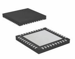
A Comprehensive Guide to LTC6409CUDB#TRMPBF ADC Driver


0.5mm 10 Amplifier LTC6409 5V 10-VFQFN Exposed Pad
This article provides a detailed overview of the LTC6409CUDB#TRMPBF ADC Driver, manufactured by Linear Technology/Analog Devices. It covers the product description, key features, primary and secondary applications, reference designs, alternative parts, and frequently asked questions to help readers understand the capabilities and potential uses of this specialized amplifier.
Product Introduction
Description:
The LTC6409CUDB#TRMPBF is a high-performance ADC driver designed for data acquisition applications. It is a specialized linear amplifier with a supply voltage of 5V and a maximum operating temperature of 70°C. With a compact 10-VFQFN Exposed Pad package and surface mount mounting type, this ADC driver offers ease of integration into various electronic systems.
Features:
- Slew Rate: 1720 V/μs
- Unity Gain Bandwidth: 8,000,000 kHz
- Average Bias Current: 160μA
- Supply Voltage Limit: 5.5V
- Input Offset Voltage: 1400μV
Applications:
Primary Applications:
1. Data Acquisition Systems: The LTC6409CUDB#TRMPBF is ideal for driving analog-to-digital converters in data acquisition systems, ensuring high-speed and accurate signal processing.
2. Communication Systems: This ADC driver can be used in communication systems to amplify signals for transmission and reception, improving overall system performance.
Secondary Applications:
1. Test and Measurement Equipment: The LTC6409CUDB#TRMPBF can enhance the performance of test and measurement instruments by providing high-speed signal amplification.
2. Industrial Automation: In industrial automation applications, this ADC driver can be used for signal conditioning and processing in control systems.
Applicable Specific Modules:
- Data acquisition modules
- Communication modules
- Test and measurement modules
- Industrial automation modules
Reference Designs:
1. Data Acquisition Board: A reference design featuring the LTC6409CUDB#TRMPBF as the ADC driver in a high-speed data acquisition board for precision measurements.
2. Communication System Module: An example reference design showcasing the integration of the LTC6409CUDB#TRMPBF in a communication system module for signal amplification.
Alternative Parts:
For applications requiring similar functionality, alternative parts to the LTC6409CUDB#TRMPBF include:
1. LTC6409-1
2. LTC6409-2
3. LTC6409-3
FAQs:
Q: What is the maximum supply voltage supported by the LTC6409CUDB#TRMPBF?
A: The LTC6409CUDB#TRMPBF has a supply voltage limit of 5.5V.
Q: What are the primary applications of the LTC6409CUDB#TRMPBF?
A: The primary applications include data acquisition systems and communication systems.
Q: Is the LTC6409CUDB#TRMPBF RoHS compliant?
A: Yes, the LTC6409CUDB#TRMPBF is RoHS3 compliant, ensuring environmental sustainability.
In conclusion, the LTC6409CUDB#TRMPBF ADC driver offers high performance and versatility for a range of applications in data acquisition, communication, test and measurement, and industrial automation systems. Its compact design, high slew rate, and low bias current make it a valuable component in modern electronic designs.
Specifications
- TypeParameter
- Factory Lead Time20 Weeks
- Mounting Type
The "Mounting Type" in electronic components refers to the method used to attach or connect a component to a circuit board or other substrate, such as through-hole, surface-mount, or panel mount.
Surface Mount - Package / Case
refers to the protective housing that encases an electronic component, providing mechanical support, electrical connections, and thermal management.
10-VFQFN Exposed Pad - Surface Mount
having leads that are designed to be soldered on the side of a circuit board that the body of the component is mounted on.
YES - Operating Temperature (Max.)70°C
- Packaging
Semiconductor package is a carrier / shell used to contain and cover one or more semiconductor components or integrated circuits. The material of the shell can be metal, plastic, glass or ceramic.
Tape & Reel (TR) - Published2010
- JESD-609 Code
The "JESD-609 Code" in electronic components refers to a standardized marking code that indicates the lead-free solder composition and finish of electronic components for compliance with environmental regulations.
e3 - Part Status
Parts can have many statuses as they progress through the configuration, analysis, review, and approval stages.
Active - Moisture Sensitivity Level (MSL)
Moisture Sensitivity Level (MSL) is a standardized rating that indicates the susceptibility of electronic components, particularly semiconductors, to moisture-induced damage during storage and the soldering process, defining the allowable exposure time to ambient conditions before they require special handling or baking to prevent failures
1 (Unlimited) - Number of Terminations10
- ECCN Code
An ECCN (Export Control Classification Number) is an alphanumeric code used by the U.S. Bureau of Industry and Security to identify and categorize electronic components and other dual-use items that may require an export license based on their technical characteristics and potential for military use.
EAR99 - TypeADC Driver
- Terminal Finish
Terminal Finish refers to the surface treatment applied to the terminals or leads of electronic components to enhance their performance and longevity. It can improve solderability, corrosion resistance, and overall reliability of the connection in electronic assemblies. Common finishes include nickel, gold, and tin, each possessing distinct properties suitable for various applications. The choice of terminal finish can significantly impact the durability and effectiveness of electronic devices.
Matte Tin (Sn) - Applications
The parameter "Applications" in electronic components refers to the specific uses or functions for which a component is designed. It encompasses various fields such as consumer electronics, industrial automation, telecommunications, automotive, and medical devices. Understanding the applications helps in selecting the right components for a particular design based on performance, reliability, and compatibility requirements. This parameter also guides manufacturers in targeting their products to relevant markets and customer needs.
Data Acquisition - HTS Code
HTS (Harmonized Tariff Schedule) codes are product classification codes between 8-1 digits. The first six digits are an HS code, and the countries of import assign the subsequent digits to provide additional classification. U.S. HTS codes are 1 digits and are administered by the U.S. International Trade Commission.
8542.33.00.01 - Terminal Position
In electronic components, the term "Terminal Position" refers to the physical location of the connection points on the component where external electrical connections can be made. These connection points, known as terminals, are typically used to attach wires, leads, or other components to the main body of the electronic component. The terminal position is important for ensuring proper connectivity and functionality of the component within a circuit. It is often specified in technical datasheets or component specifications to help designers and engineers understand how to properly integrate the component into their circuit designs.
QUAD - Terminal Form
Occurring at or forming the end of a series, succession, or the like; closing; concluding.
NO LEAD - Peak Reflow Temperature (Cel)
Peak Reflow Temperature (Cel) is a parameter that specifies the maximum temperature at which an electronic component can be exposed during the reflow soldering process. Reflow soldering is a common method used to attach electronic components to a circuit board. The Peak Reflow Temperature is crucial because it ensures that the component is not damaged or degraded during the soldering process. Exceeding the specified Peak Reflow Temperature can lead to issues such as component failure, reduced performance, or even permanent damage to the component. It is important for manufacturers and assemblers to adhere to the recommended Peak Reflow Temperature to ensure the reliability and functionality of the electronic components.
NOT SPECIFIED - Number of Functions1
- Supply Voltage
Supply voltage refers to the electrical potential difference provided to an electronic component or circuit. It is crucial for the proper operation of devices, as it powers their functions and determines performance characteristics. The supply voltage must be within specified limits to ensure reliability and prevent damage to components. Different electronic devices have specific supply voltage requirements, which can vary widely depending on their design and intended application.
5V - Terminal Pitch
The center distance from one pole to the next.
0.5mm - Time@Peak Reflow Temperature-Max (s)
Time@Peak Reflow Temperature-Max (s) refers to the maximum duration that an electronic component can be exposed to the peak reflow temperature during the soldering process, which is crucial for ensuring reliable solder joint formation without damaging the component.
NOT SPECIFIED - Base Part Number
The "Base Part Number" (BPN) in electronic components serves a similar purpose to the "Base Product Number." It refers to the primary identifier for a component that captures the essential characteristics shared by a group of similar components. The BPN provides a fundamental way to reference a family or series of components without specifying all the variations and specific details.
LTC6409 - Pin Count
a count of all of the component leads (or pins)
10 - JESD-30 Code
JESD-30 Code refers to a standardized descriptive designation system established by JEDEC for semiconductor-device packages. This system provides a systematic method for generating designators that convey essential information about the package's physical characteristics, such as size and shape, which aids in component identification and selection. By using JESD-30 codes, manufacturers and engineers can ensure consistency and clarity in the specification of semiconductor packages across various applications and industries.
R-PQCC-N10 - Qualification Status
An indicator of formal certification of qualifications.
Not Qualified - Temperature Grade
Temperature grades represent a tire's resistance to heat and its ability to dissipate heat when tested under controlled laboratory test conditions.
COMMERCIAL - Slew Rate
the maximum rate of output voltage change per unit time.
1720 V/us - Unity Gain BW-Nom
Unity Gain Bandwidth, often abbreviated as Unity Gain BW or UGBW, refers to the frequency at which an amplifier can provide a gain of one (0 dB). It is a critical parameter in assessing the performance of operational amplifiers and other amplifying devices, indicating the range of frequencies over which the amplifier can operate without distortion. Unity Gain BW is particularly important in applications where signal fidelity is crucial, as it helps determine the maximum frequency of operation for a given gain level. As the gain is reduced, the bandwidth typically increases, ensuring that the amplifier can still operate effectively across various signal frequencies.
8000000 kHz - Average Bias Current-Max (IIB)
The parameter "Average Bias Current-Max (IIB)" in electronic components refers to the maximum average bias current that the component can handle without exceeding its specified operating limits. Bias current is the current that flows through a component when it is in its quiescent state or when it is not actively processing a signal. Exceeding the maximum average bias current can lead to overheating, reduced performance, or even damage to the component. Therefore, it is important to ensure that the bias current does not exceed the specified maximum value to maintain the reliability and longevity of the electronic component.
160μA - Supply Voltage Limit-Max
The parameter "Supply Voltage Limit-Max" in electronic components refers to the maximum voltage that the component can safely handle without getting damaged. This specification is crucial for ensuring the reliable operation and longevity of the component within a given electrical system. Exceeding the maximum supply voltage limit can lead to overheating, electrical breakdown, or permanent damage to the component. It is important to carefully adhere to this limit when designing and operating electronic circuits to prevent potential failures and ensure the overall system's performance and safety.
5.5V - Input Offset Voltage-Max
The parameter "Input Offset Voltage-Max" in electronic components refers to the maximum allowable difference in voltage between the input terminals of an operational amplifier or other analog circuitry before the output is affected. It is a measure of the device's ability to maintain precise and accurate signal processing. A higher Input Offset Voltage-Max value indicates a greater potential for error in the output signal due to input voltage differences. Designers must consider this parameter when selecting components to ensure the desired level of accuracy and performance in their circuits.
1400μV - Length3mm
- Height Seated (Max)
Height Seated (Max) is a parameter in electronic components that refers to the maximum allowable height of the component when it is properly seated or installed on a circuit board or within an enclosure. This specification is crucial for ensuring proper fit and alignment within the overall system design. Exceeding the maximum seated height can lead to mechanical interference, electrical shorts, or other issues that may impact the performance and reliability of the electronic device. Manufacturers provide this information to help designers and engineers select components that will fit within the designated space and function correctly in the intended application.
0.85mm - Width2mm
- RoHS Status
RoHS means “Restriction of Certain Hazardous Substances” in the “Hazardous Substances Directive” in electrical and electronic equipment.
ROHS3 Compliant
Parts with Similar Specs
Datasheet PDF
- Datasheets :
 LM7805CT Voltage Regulator: Feature, Specification, and Datasheet
16 June 20215163
 LPS53 vs NPS63-M-006
11 January 2022409
 OPTIREG™ linear TLE4267 400mA LDO: Solving Automotive Power Stability and Thermal Challenges
04 June 2026329
 CS43131 High-Performance DAC, 32-Bit Audio D/A Converters and Pinout
10 January 20229632
 KSZ8081MNX Transceiver: Pinout, Equivalent and Datasheet
24 January 20223037
 TIP117 PNP Power Transistor: Datasheet pdf, STM Darlington transistor
21 December 20213073
![IRF9540 Power MOSFET: IRF9540 Datasheet, Pinout, Equivalent [FAQ&Video]](https://res.utmel.com/Images/Article/12c54825-fa2a-4d26-a483-fcf810425cd9.jpg) IRF9540 Power MOSFET: IRF9540 Datasheet, Pinout, Equivalent [FAQ&Video]
IRF9540 Power MOSFET: IRF9540 Datasheet, Pinout, Equivalent [FAQ&Video]17 December 202114710
 PT4115 High Brightness LED Driver: 30A, 1.2V Step-down Driver, Equivalent and Pinout
06 January 202215607
 New Crisis in Semiconductors: Neon Gas Prices Soar 9 Times
21 March 20229292
 15 Key Elements of Diode Selection
26 November 202118867
 SR626SW Battery Equivalent: Technical Specs, Chemistries, and Selection Guide
26 May 2026817
 A $39 Billion Investment Wave Expected to Boost AI and Semiconductor Stocks
26 September 20232645
 The Difference and Application of SPI, UART, I2C Communication
15 October 202511839
 How Many Smart Sensors Should a Car Be Equipped With?
28 March 20224725
 Semiconductor Veteran Kevin Conley Takes Helm as CEO of Applied Brain Research
13 September 20233703
 How Do We Seize Investment Opportunities on the Eve of the Ultimate Human Energy Final?
12 July 20222226
Linear Technology/Analog Devices
In Stock
United States
China
Canada
Japan
Russia
Germany
United Kingdom
Singapore
Italy
Hong Kong(China)
Taiwan(China)
France
Korea
Mexico
Netherlands
Malaysia
Austria
Spain
Switzerland
Poland
Thailand
Vietnam
India
United Arab Emirates
Afghanistan
Åland Islands
Albania
Algeria
American Samoa
Andorra
Angola
Anguilla
Antigua & Barbuda
Argentina
Armenia
Aruba
Australia
Azerbaijan
Bahamas
Bahrain
Bangladesh
Barbados
Belarus
Belgium
Belize
Benin
Bermuda
Bhutan
Bolivia
Bonaire, Sint Eustatius and Saba
Bosnia & Herzegovina
Botswana
Brazil
British Indian Ocean Territory
British Virgin Islands
Brunei
Bulgaria
Burkina Faso
Burundi
Cabo Verde
Cambodia
Cameroon
Cayman Islands
Central African Republic
Chad
Chile
Christmas Island
Cocos (Keeling) Islands
Colombia
Comoros
Congo
Congo (DRC)
Cook Islands
Costa Rica
Côte d’Ivoire
Croatia
Cuba
Curaçao
Cyprus
Czechia
Denmark
Djibouti
Dominica
Dominican Republic
Ecuador
Egypt
El Salvador
Equatorial Guinea
Eritrea
Estonia
Eswatini
Ethiopia
Falkland Islands
Faroe Islands
Fiji
Finland
French Guiana
French Polynesia
Gabon
Gambia
Georgia
Ghana
Gibraltar
Greece
Greenland
Grenada
Guadeloupe
Guam
Guatemala
Guernsey
Guinea
Guinea-Bissau
Guyana
Haiti
Honduras
Hungary
Iceland
Indonesia
Iran
Iraq
Ireland
Isle of Man
Israel
Jamaica
Jersey
Jordan
Kazakhstan
Kenya
Kiribati
Kosovo
Kuwait
Kyrgyzstan
Laos
Latvia
Lebanon
Lesotho
Liberia
Libya
Liechtenstein
Lithuania
Luxembourg
Macao(China)
Madagascar
Malawi
Maldives
Mali
Malta
Marshall Islands
Martinique
Mauritania
Mauritius
Mayotte
Micronesia
Moldova
Monaco
Mongolia
Montenegro
Montserrat
Morocco
Mozambique
Myanmar
Namibia
Nauru
Nepal
New Caledonia
New Zealand
Nicaragua
Niger
Nigeria
Niue
Norfolk Island
North Korea
North Macedonia
Northern Mariana Islands
Norway
Oman
Pakistan
Palau
Palestinian Authority
Panama
Papua New Guinea
Paraguay
Peru
Philippines
Pitcairn Islands
Portugal
Puerto Rico
Qatar
Réunion
Romania
Rwanda
Samoa
San Marino
São Tomé & Príncipe
Saudi Arabia
Senegal
Serbia
Seychelles
Sierra Leone
Sint Maarten
Slovakia
Slovenia
Solomon Islands
Somalia
South Africa
South Sudan
Sri Lanka
St Helena, Ascension, Tristan da Cunha
St. Barthélemy
St. Kitts & Nevis
St. Lucia
St. Martin
St. Pierre & Miquelon
St. Vincent & Grenadines
Sudan
Suriname
Svalbard & Jan Mayen
Sweden
Syria
Tajikistan
Tanzania
Timor-Leste
Togo
Tokelau
Tonga
Trinidad & Tobago
Tunisia
Turkey
Turkmenistan
Turks & Caicos Islands
Tuvalu
U.S. Outlying Islands
U.S. Virgin Islands
Uganda
Ukraine
Uruguay
Uzbekistan
Vanuatu
Vatican City
Venezuela
Wallis & Futuna
Yemen
Zambia
Zimbabwe
![AD8138ARZ]() AD8138ARZ
AD8138ARZAnalog Devices Inc.
![AD8138ARMZ]() AD8138ARMZ
AD8138ARMZAnalog Devices Inc.
![AD8310ARMZ]() AD8310ARMZ
AD8310ARMZAnalog Devices Inc.
![ADA4941-1YRZ]() ADA4941-1YRZ
ADA4941-1YRZAnalog Devices Inc.
![AD8309ARUZ]() AD8309ARUZ
AD8309ARUZAnalog Devices Inc.
![AD8331ARQZ]() AD8331ARQZ
AD8331ARQZAnalog Devices Inc.
![AD8138ARZ-R7]() AD8138ARZ-R7
AD8138ARZ-R7Analog Devices Inc.
![AD8138ARMZ-REEL7]() AD8138ARMZ-REEL7
AD8138ARMZ-REEL7Analog Devices Inc.
![AD8310ARMZ-REEL7]() AD8310ARMZ-REEL7
AD8310ARMZ-REEL7Analog Devices Inc.
![AD8307ARZ]() AD8307ARZ
AD8307ARZAnalog Devices Inc.


