
 Product
 Brand
Brand Articles
 Tools
Tools
MX25R8035FZUIL0 Flash Memory: Features, Pinout, and Datasheet


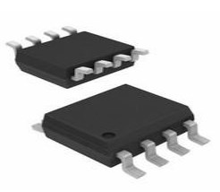
MXSMIO™ Memory IC MXSMIO™ Series 3mm mm
MX25R8035F is an 8MB Serial NOR Flash memory with an internal configuration of 1,048,576 x 8. The structure becomes 2,097,152 bits x 4 or 4,194,304 bits x 2 when it is in four I/O modes. This article mainly introduces features, pinout, datasheet and other detailed information about Macronix MX25R8035FZUIL0.

What Is Flash Memory?
MX25R8035FZUIL0 Description
MX25R8035F is an 8MB Serial NOR Flash memory with an internal configuration of 1,048,576 x 8. The structure becomes 2,097,152 bits x 4 or 4,194,304 bits x 2 when it is in four I/O mode.
In single I/O mode, the MX25R8035F has a serial peripheral interface and software protocol that allows it to operate on a basic 3-wire bus. A clock input (SCLK), a serial data input (SI), and a serial data output (SDO) are the three bus signals (SO). CS# input allows serial access to the device.
The SI and SO pins become SIO0 and SIO1 pins for address/dummy bits input and data output when it is in two I/O read modes. The SI pin, SO pin, WP# pin, and RESET#/HOLD# pin become SIO0 pin, SIO1 pin, SIO2 pin, and SIO3 pin for address/dummy bits input and data output when it is in four I/O read mode.
On the full chip, the MX25R8035F MXSMIO® (Serial Multi I/O) allows sequential read operation.
After issuing the program/erase command, auto program/erase algorithms will be executed, which will program/erase and validate the given page, sector, or block locations. The program command is carried out on a byte, page (256 bytes), or word basis. The Erase command can be used to erase a 4K-byte sector, a 32K-byte block, a 64K-byte block, or the entire chip.
A status register is included to improve user convenience by indicating the chip's status. The status read command can be used to determine whether a program or erase operation is complete using the WIP bit.
Advanced security features improve the protection and security functions; for more information, read the security features section .
The MX25R8035F utilizes Macronix 's proprietary memory cell, which reliably stores memory contents even after 100,000 program and erase cycles.
MX25R8035FZUIL0 Pinout
The following figure is MX25R8035FZUIL0 Pinout.

Pinout
| Pin Number | Pin Name | Description |
| 1 | CS# | Chip Select |
| 5 | SI/SIO0 | Serial Data Input (for 1 x I/O)/ Serial Data Input & Output (for 4xI/O read mode) |
| 2 | SO/SIO1 | Serial Data Output (for 1 x I/O)/ Serial Data Input & Output (for 4xI/O read mode) |
| 6 | SCLK | Clock Input |
| 3 | WP#/SIO2 | Write Protection Active Low or Serial Data Input & Output (for 4xI/O read mode) |
| 7 | RESET#/SIO3 * | Hardware Reset Pin Active low or Serial Data Input & Output (for 4xI/O read mode) |
| HOLD#/SIO3 * | To pause the device without deselecting the device or Serial Data Input & Output (for 4xI/O read m | |
| 8 | VCC | Power Supply |
| 4 | GND | Ground |
MX25R8035FZUIL0 CAD Model


MX25R8035FZUIL0 Features
• Ultra-Low Power Mode and High-Performance Mode
• Wide Range VCC 1.65V-3.6V for Read, Erase and Program Operations
• Unique ID and Secure OTP Support
• Multi I/O Support - Single I/O, Dual I/O and Quad I/O
• Program Suspend/Resume & Erase Suspend/Resume
Specifications
- TypeParameter
- Factory Lead Time10 Weeks
- Mounting Type
The "Mounting Type" in electronic components refers to the method used to attach or connect a component to a circuit board or other substrate, such as through-hole, surface-mount, or panel mount.
Surface Mount - Package / Case
refers to the protective housing that encases an electronic component, providing mechanical support, electrical connections, and thermal management.
8-UFDFN Exposed Pad - Surface Mount
having leads that are designed to be soldered on the side of a circuit board that the body of the component is mounted on.
YES - Memory TypesNon-Volatile
- Operating Temperature
The operating temperature is the range of ambient temperature within which a power supply, or any other electrical equipment, operate in. This ranges from a minimum operating temperature, to a peak or maximum operating temperature, outside which, the power supply may fail.
-40°C~85°C TA - Packaging
Semiconductor package is a carrier / shell used to contain and cover one or more semiconductor components or integrated circuits. The material of the shell can be metal, plastic, glass or ceramic.
Cut Tape (CT) - Series
In electronic components, the "Series" refers to a group of products that share similar characteristics, designs, or functionalities, often produced by the same manufacturer. These components within a series typically have common specifications but may vary in terms of voltage, power, or packaging to meet different application needs. The series name helps identify and differentiate between various product lines within a manufacturer's catalog.
MXSMIO™ - Published2017
- Part Status
Parts can have many statuses as they progress through the configuration, analysis, review, and approval stages.
Active - Moisture Sensitivity Level (MSL)
Moisture Sensitivity Level (MSL) is a standardized rating that indicates the susceptibility of electronic components, particularly semiconductors, to moisture-induced damage during storage and the soldering process, defining the allowable exposure time to ambient conditions before they require special handling or baking to prevent failures
3 (168 Hours) - Number of Terminations8
- Additional Feature
Any Feature, including a modified Existing Feature, that is not an Existing Feature.
IT IS ALSO CONFIGURED AS 8M X 1 - Voltage - Supply
Voltage - Supply refers to the range of voltage levels that an electronic component or circuit is designed to operate with. It indicates the minimum and maximum supply voltage that can be applied for the device to function properly. Providing supply voltages outside this range can lead to malfunction, damage, or reduced performance. This parameter is critical for ensuring compatibility between different components in a circuit.
1.65V~3.6V - Terminal Position
In electronic components, the term "Terminal Position" refers to the physical location of the connection points on the component where external electrical connections can be made. These connection points, known as terminals, are typically used to attach wires, leads, or other components to the main body of the electronic component. The terminal position is important for ensuring proper connectivity and functionality of the component within a circuit. It is often specified in technical datasheets or component specifications to help designers and engineers understand how to properly integrate the component into their circuit designs.
DUAL - Peak Reflow Temperature (Cel)
Peak Reflow Temperature (Cel) is a parameter that specifies the maximum temperature at which an electronic component can be exposed during the reflow soldering process. Reflow soldering is a common method used to attach electronic components to a circuit board. The Peak Reflow Temperature is crucial because it ensures that the component is not damaged or degraded during the soldering process. Exceeding the specified Peak Reflow Temperature can lead to issues such as component failure, reduced performance, or even permanent damage to the component. It is important for manufacturers and assemblers to adhere to the recommended Peak Reflow Temperature to ensure the reliability and functionality of the electronic components.
NOT SPECIFIED - Number of Functions1
- Supply Voltage
Supply voltage refers to the electrical potential difference provided to an electronic component or circuit. It is crucial for the proper operation of devices, as it powers their functions and determines performance characteristics. The supply voltage must be within specified limits to ensure reliability and prevent damage to components. Different electronic devices have specific supply voltage requirements, which can vary widely depending on their design and intended application.
1.8V - Terminal Pitch
The center distance from one pole to the next.
0.5mm - Time@Peak Reflow Temperature-Max (s)
Time@Peak Reflow Temperature-Max (s) refers to the maximum duration that an electronic component can be exposed to the peak reflow temperature during the soldering process, which is crucial for ensuring reliable solder joint formation without damaging the component.
NOT SPECIFIED - JESD-30 Code
JESD-30 Code refers to a standardized descriptive designation system established by JEDEC for semiconductor-device packages. This system provides a systematic method for generating designators that convey essential information about the package's physical characteristics, such as size and shape, which aids in component identification and selection. By using JESD-30 codes, manufacturers and engineers can ensure consistency and clarity in the specification of semiconductor packages across various applications and industries.
R-PDSO-N8 - Supply Voltage-Max (Vsup)
The parameter "Supply Voltage-Max (Vsup)" in electronic components refers to the maximum voltage that can be safely applied to the component without causing damage. It is an important specification to consider when designing or using electronic circuits to ensure the component operates within its safe operating limits. Exceeding the maximum supply voltage can lead to overheating, component failure, or even permanent damage. It is crucial to adhere to the specified maximum supply voltage to ensure the reliable and safe operation of the electronic component.
3.6V - Supply Voltage-Min (Vsup)
The parameter "Supply Voltage-Min (Vsup)" in electronic components refers to the minimum voltage level required for the component to operate within its specified performance range. This parameter indicates the lowest voltage that can be safely applied to the component without risking damage or malfunction. It is crucial to ensure that the supply voltage provided to the component meets or exceeds this minimum value to ensure proper functionality and reliability. Failure to adhere to the specified minimum supply voltage may result in erratic behavior, reduced performance, or even permanent damage to the component.
1.65V - Memory Size
The memory capacity is the amount of data a device can store at any given time in its memory.
8Mb 1M x 8 - Operating Mode
A phase of operation during the operation and maintenance stages of the life cycle of a facility.
SYNCHRONOUS - Clock Frequency
Clock frequency, also known as clock speed, refers to the rate at which a processor or electronic component can execute instructions. It is measured in hertz (Hz) and represents the number of cycles per second that the component can perform. A higher clock frequency typically indicates a faster processing speed and better performance. However, it is important to note that other factors such as architecture, efficiency, and workload also play a significant role in determining the overall performance of a component. In summary, clock frequency is a crucial parameter that influences the speed and efficiency of electronic components in processing data and executing tasks.
33MHz - Access Time
Access time in electronic components refers to the amount of time it takes for a system to retrieve data from memory or storage once a request has been made. It is typically measured in nanoseconds or microseconds and indicates the speed at which data can be accessed. Lower access time values signify faster performance, allowing for more efficient processing in computing systems. Access time is a critical parameter in determining the overall responsiveness of electronic devices, particularly in applications requiring quick data retrieval.
12 ns - Memory Format
Memory Format in electronic components refers to the specific organization and structure of data storage within a memory device. It defines how data is stored, accessed, and managed within the memory module. Different memory formats include RAM (Random Access Memory), ROM (Read-Only Memory), and various types of flash memory. The memory format determines the speed, capacity, and functionality of the memory device, and it is crucial for compatibility with other components in a system. Understanding the memory format is essential for selecting the right memory module for a particular application or device.
FLASH - Memory Interface
An external memory interface is a bus protocol for communication from an integrated circuit, such as a microprocessor, to an external memory device located on a circuit board.
SPI - Organization
In the context of electronic components, the parameter "Organization" typically refers to the arrangement or structure of the internal components within a device or system. It can describe how various elements such as transistors, resistors, capacitors, and other components are physically arranged and interconnected on a circuit board or within a semiconductor chip.The organization of electronic components plays a crucial role in determining the functionality, performance, and efficiency of a device. It can impact factors such as signal propagation, power consumption, thermal management, and overall system complexity. Engineers carefully design the organization of components to optimize the operation of electronic devices and ensure reliable performance.Different types of electronic components may have specific organizational requirements based on the intended application and design considerations. For example, integrated circuits may have a highly compact and intricate organization to maximize functionality within a small footprint, while larger electronic systems may have a more modular and distributed organization to facilitate maintenance and scalability.
2MX4 - Memory Width
Memory width refers to the number of bits that can be read or written to memory at one time. It is an important specification in electronic components, particularly in memory devices like RAM and cache. A wider memory width allows for greater data throughput, enabling faster performance as more data can be processed simultaneously. Memory width can vary among different types of memory and can impact both the complexity and efficiency of data handling within electronic systems.
4 - Write Cycle Time - Word, Page
Write Cycle Time - Word, Page refers to the duration required to write data to a specific memory cell or a page of memory in electronic components, particularly in non-volatile memories like Flash or EEPROM. It indicates the time taken to complete a writing operation for a single word or an entire page of data. This parameter is crucial for determining the performance and speed of memory devices in applications where quick data storage is essential. It impacts the overall efficiency in data handling, affecting both read and write speeds in memory-related operations.
100μs, 10ms - Memory Density
Memory density in electronic components refers to the amount of data that can be stored in a given physical space or memory module. It is typically measured in bits or bytes per unit area, such as bits per square inch. Higher memory density means that more data can be stored in a smaller space, which is important for devices with limited physical size or power constraints. Memory density is a key factor in determining the capacity and performance of memory devices, such as RAM, ROM, and flash memory, and is a critical consideration in the design and manufacturing of electronic products.
8388608 bit - Parallel/Serial
The parameter "Parallel/Serial" in electronic components refers to the method of data transmission or communication within the component. In parallel communication, multiple bits of data are transmitted simultaneously over multiple channels or wires. This allows for faster data transfer rates but requires more physical connections and can be more susceptible to signal interference.On the other hand, in serial communication, data is transmitted sequentially over a single channel or wire. While serial communication may have slower data transfer rates compared to parallel communication, it is more cost-effective, requires fewer connections, and is less prone to signal interference.The choice between parallel and serial communication depends on the specific requirements of the electronic component and the overall system design, balancing factors such as speed, cost, complexity, and reliability.
SERIAL - Programming Voltage
A special high-voltage supply that supplies the potential and energy for altering the state of certain nonvolatile memory arrays. On some devices, the presence of VPP also acts as a program enable signal (P).
1.8V - Alternate Memory Width
Alternate Memory Width is a parameter in electronic components that refers to the ability of a memory device to operate with different data bus widths. This means that the memory device can support various configurations of data bus widths, allowing for flexibility in system design and compatibility with different applications. By offering alternate memory widths, the device can be used in a wider range of systems without requiring significant changes to the overall design. This parameter is important for optimizing performance and efficiency in electronic systems by providing options for data transfer and storage based on specific requirements.
2 - Ambient Temperature Range High
This varies from person to person, but it is somewhere between 68 and 77 degrees F on average. The temperature setting that is comfortable for an individual may fluctuate with humidity and outside temperature as well. The temperature of an air conditioned room can also be considered ambient temperature.
85°C - Height600μm
- Length3mm
- Width2mm
- RoHS Status
RoHS means “Restriction of Certain Hazardous Substances” in the “Hazardous Substances Directive” in electrical and electronic equipment.
ROHS3 Compliant - Lead Free
Lead Free is a term used to describe electronic components that do not contain lead as part of their composition. Lead is a toxic material that can have harmful effects on human health and the environment, so the electronics industry has been moving towards lead-free components to reduce these risks. Lead-free components are typically made using alternative materials such as silver, copper, and tin. Manufacturers must comply with regulations such as the Restriction of Hazardous Substances (RoHS) directive to ensure that their products are lead-free and environmentally friendly.
Lead Free
MX25R8035FZUIL0 Functional Block Diagram
MX25R8035FZUIL0 Functional Block Diagram is shown as follows.

Functional Block Diagram
MX25R8035FZUIL0 Part Name Description

MX25R8035FZUIL0 Package

MX25R8035FZUIL0 Manufacturer
Macronix, a prominent non-volatile memory (NVM) integrated device maker, offers a full range of NOR Flash, NAND Flash, and ROM solutions. Macronix continues to provide high-quality, innovative, and performance-driven products to its clients in the consumer, communication, computer, automotive, networking, and other segment markets, thanks to its world-class R&D and manufacturing capabilities.
Trend Analysis
Datasheet PDF
- PCN Packaging :
- Datasheets :
Is flash memory RAM or ROM?
Is Flash memory RAM or ROM? RAM is Read-Only Memory. Unlike RAM, ROM is persistent storage. Flash Memory is one category of ROM i.e Electrically Erasable Read Only Memory (EEPROM).
What is flash memory and how does it work?
Flash memory is a type of erasable read-only memory (EEPROM) that clears and rewrites data in chunks for fast, energy-efficient access and rewriting. Flash memory, or flash storage, is non-volatile, which means it remains viable even without an active power source.
Why is it called flash memory?
According to Toshiba, the name "flash" was suggested by Masuoka's colleague, Shōji Ariizumi, because the erasure process of the memory contents reminded him of the flash of a camera.
 Arduino Uno R4 WiFi: Description, Features and applications
06 October 20235449
 NTE987 Operational Amplifier: Datasheet, Pinout and Equivalent
16 September 20212444
 MMBT2222A NPN Purpose Transistor: Datasheet, Pinout and Equivalents
14 October 20213173
 STM32G0 Microcontroller: Pinout, Diagram and Datasheet
29 September 20218309
 ATTINY45 Microcontroller: Pinout, Specifications and Datasheet
19 October 20215464
 STSPIN32F0 BLDC Controller: Features, Applications and Datasheet
20 November 20231643
 AD260BND-1 Digital Isolators: Pinout, Specification, Datasheet
14 August 2024453
 Exploring the STM32L083xx Ultra-Low-Power 32-bit MCU
29 February 2024165
 Diodes Tutorial: How to Test Diodes?
22 October 20259884
 Basic Introduction to Metal Film Resistor
28 August 202013073
 A Hybrid SiC and GaN-Based DC-DC Converter for EVs
20 September 20242408
 Varistor: Definition, Function, Working and Testing
03 April 202581587
 SIA's Latest Report: Status and Challenges of US Semiconductors
22 February 20232840
 What is a Switched Reluctance Motor?
09 July 20248033
 Increasing the Efficiency through Wide-Bandgap Semiconductors (SiC & GaN)
24 October 20222419
 Introduction to TTL and CMOS Logic Gate Circuits
24 November 202520406
Macronix
In Stock: 25286
United States
China
Canada
Japan
Russia
Germany
United Kingdom
Singapore
Italy
Hong Kong(China)
Taiwan(China)
France
Korea
Mexico
Netherlands
Malaysia
Austria
Spain
Switzerland
Poland
Thailand
Vietnam
India
United Arab Emirates
Afghanistan
Åland Islands
Albania
Algeria
American Samoa
Andorra
Angola
Anguilla
Antigua & Barbuda
Argentina
Armenia
Aruba
Australia
Azerbaijan
Bahamas
Bahrain
Bangladesh
Barbados
Belarus
Belgium
Belize
Benin
Bermuda
Bhutan
Bolivia
Bonaire, Sint Eustatius and Saba
Bosnia & Herzegovina
Botswana
Brazil
British Indian Ocean Territory
British Virgin Islands
Brunei
Bulgaria
Burkina Faso
Burundi
Cabo Verde
Cambodia
Cameroon
Cayman Islands
Central African Republic
Chad
Chile
Christmas Island
Cocos (Keeling) Islands
Colombia
Comoros
Congo
Congo (DRC)
Cook Islands
Costa Rica
Côte d’Ivoire
Croatia
Cuba
Curaçao
Cyprus
Czechia
Denmark
Djibouti
Dominica
Dominican Republic
Ecuador
Egypt
El Salvador
Equatorial Guinea
Eritrea
Estonia
Eswatini
Ethiopia
Falkland Islands
Faroe Islands
Fiji
Finland
French Guiana
French Polynesia
Gabon
Gambia
Georgia
Ghana
Gibraltar
Greece
Greenland
Grenada
Guadeloupe
Guam
Guatemala
Guernsey
Guinea
Guinea-Bissau
Guyana
Haiti
Honduras
Hungary
Iceland
Indonesia
Iran
Iraq
Ireland
Isle of Man
Israel
Jamaica
Jersey
Jordan
Kazakhstan
Kenya
Kiribati
Kosovo
Kuwait
Kyrgyzstan
Laos
Latvia
Lebanon
Lesotho
Liberia
Libya
Liechtenstein
Lithuania
Luxembourg
Macao(China)
Madagascar
Malawi
Maldives
Mali
Malta
Marshall Islands
Martinique
Mauritania
Mauritius
Mayotte
Micronesia
Moldova
Monaco
Mongolia
Montenegro
Montserrat
Morocco
Mozambique
Myanmar
Namibia
Nauru
Nepal
New Caledonia
New Zealand
Nicaragua
Niger
Nigeria
Niue
Norfolk Island
North Korea
North Macedonia
Northern Mariana Islands
Norway
Oman
Pakistan
Palau
Palestinian Authority
Panama
Papua New Guinea
Paraguay
Peru
Philippines
Pitcairn Islands
Portugal
Puerto Rico
Qatar
Réunion
Romania
Rwanda
Samoa
San Marino
São Tomé & Príncipe
Saudi Arabia
Senegal
Serbia
Seychelles
Sierra Leone
Sint Maarten
Slovakia
Slovenia
Solomon Islands
Somalia
South Africa
South Sudan
Sri Lanka
St Helena, Ascension, Tristan da Cunha
St. Barthélemy
St. Kitts & Nevis
St. Lucia
St. Martin
St. Pierre & Miquelon
St. Vincent & Grenadines
Sudan
Suriname
Svalbard & Jan Mayen
Sweden
Syria
Tajikistan
Tanzania
Timor-Leste
Togo
Tokelau
Tonga
Trinidad & Tobago
Tunisia
Turkey
Turkmenistan
Turks & Caicos Islands
Tuvalu
U.S. Outlying Islands
U.S. Virgin Islands
Uganda
Ukraine
Uruguay
Uzbekistan
Vanuatu
Vatican City
Venezuela
Wallis & Futuna
Yemen
Zambia
Zimbabwe
![MX25L12873FM2I-10G]() MX25L12873FM2I-10G
MX25L12873FM2I-10GMacronix
![MX25L25673GMI-10G]() MX25L25673GMI-10G
MX25L25673GMI-10GMacronix
![MX30UF4G18AC-TI]() MX30UF4G18AC-TI
MX30UF4G18AC-TIMacronix
![MX25L3206EZUI-12G]() MX25L3206EZUI-12G
MX25L3206EZUI-12GMacronix
![MX25L12835FM2I-10G]() MX25L12835FM2I-10G
MX25L12835FM2I-10GMacronix
![MX25L6406EM2I-12G]() MX25L6406EM2I-12G
MX25L6406EM2I-12GMacronix
![MX25R6435FM2IL0]() MX25R6435FM2IL0
MX25R6435FM2IL0Macronix
![MX25L12835FMI-10G]() MX25L12835FMI-10G
MX25L12835FMI-10GMacronix
![MX29GL256FHT2I-90Q]() MX29GL256FHT2I-90Q
MX29GL256FHT2I-90QMacronix
![MX29LV320EBTI-70G]() MX29LV320EBTI-70G
MX29LV320EBTI-70GMacronix


