
 Product
 Brand
Brand Articles
 Tools
Tools
A Comprehensive Guide to S-8333AAEB-T8T1G DC-DC Switching Controller

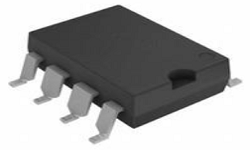
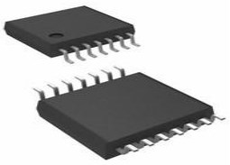
8 Terminals 1.8V~6V DC to DC converter IC SWITCHING CONTROLLER 1 Outputs 280kHz~1.08MHz Transistor Driver
Unit Price: $0.834998
Ext Price: $0.83


8 Terminals 1.8V~6V DC to DC converter IC SWITCHING CONTROLLER 1 Outputs 280kHz~1.08MHz Transistor Driver
This article provides a detailed overview of the S-8333AAEB-T8T1G DC-DC switching controller manufactured by ABLIC U.S.A. Inc. It covers the product description, key features, primary and secondary applications, reference designs, alternative parts, and frequently asked questions related to this voltage regulator.
Product Introduction
Description:
The S-8333AAEB-T8T1G is a DC-DC switching controller designed for step-up applications, with a voltage input range of 1.8V to 6V. It features a boost topology, operating at a switching frequency range of 280kHz to 1.08MHz. The controller incorporates current limit and frequency control functions to regulate the output voltage efficiently.
Features:
- Input Voltage Range: 1.8V to 6V
- Output Type: Transistor Driver
- Control Features: Current Limit, Frequency Control
- Topology: Boost
- Switching Frequency: 280kHz to 1.08MHz
- Duty Cycle: Up to 89%
- Package: 8-TSSOP (Surface Mount)
- RoHS Compliant
Applications:
Primary Applications:
1. Portable Electronic Devices
2. Battery-Powered Systems
3. LED Backlighting
4. IoT Devices
Secondary Applications:
1. Power Banks
2. Wearable Devices
3. Solar-Powered Systems
4. Automotive Electronics
Applicable Specific Modules:
1. Power Management Modules
2. LED Driver Modules
3. Battery Charging Modules
Reference Designs:
1. Portable Solar Charger
2. Wearable Health Monitor
3. LED Flashlight
4. IoT Sensor Node
Alternative Parts:
1. S-8333ABEB-T8T1G
2. S-8333ACDB-T8T1G
3. S-8333AEEB-T8T1G
FAQs:
Q1: What is the maximum input voltage supported by the S-8333AAEB-T8T1G?
A1: The maximum input voltage for this DC-DC switching controller is 6V.
Q2: Does the S-8333AAEB-T8T1G support synchronous rectification?
A2: No, this controller does not feature synchronous rectification.
Q3: What is the duty cycle range of the S-8333AAEB-T8T1G?
A3: The duty cycle can be as high as 89% for this switching controller.
In conclusion, the S-8333AAEB-T8T1G DC-DC switching controller offers a versatile solution for various step-up voltage applications with its compact design and efficient performance. Its features, applications, and compatibility with alternative parts make it a suitable choice for modern electronic systems requiring voltage regulation.
Specifications
- TypeParameter
- Mounting Type
The "Mounting Type" in electronic components refers to the method used to attach or connect a component to a circuit board or other substrate, such as through-hole, surface-mount, or panel mount.
Surface Mount - Package / Case
refers to the protective housing that encases an electronic component, providing mechanical support, electrical connections, and thermal management.
8-TSSOP (0.173, 4.40mm Width) - Surface Mount
having leads that are designed to be soldered on the side of a circuit board that the body of the component is mounted on.
YES - Operating Temperature
The operating temperature is the range of ambient temperature within which a power supply, or any other electrical equipment, operate in. This ranges from a minimum operating temperature, to a peak or maximum operating temperature, outside which, the power supply may fail.
-40°C~85°C TA - Packaging
Semiconductor package is a carrier / shell used to contain and cover one or more semiconductor components or integrated circuits. The material of the shell can be metal, plastic, glass or ceramic.
Tape & Reel (TR) - JESD-609 Code
The "JESD-609 Code" in electronic components refers to a standardized marking code that indicates the lead-free solder composition and finish of electronic components for compliance with environmental regulations.
e6 - Pbfree Code
The "Pbfree Code" parameter in electronic components refers to the code or marking used to indicate that the component is lead-free. Lead (Pb) is a toxic substance that has been widely used in electronic components for many years, but due to environmental concerns, there has been a shift towards lead-free alternatives. The Pbfree Code helps manufacturers and users easily identify components that do not contain lead, ensuring compliance with regulations and promoting environmentally friendly practices. It is important to pay attention to the Pbfree Code when selecting electronic components to ensure they meet the necessary requirements for lead-free applications.
yes - Part Status
Parts can have many statuses as they progress through the configuration, analysis, review, and approval stages.
Not For New Designs - Moisture Sensitivity Level (MSL)
Moisture Sensitivity Level (MSL) is a standardized rating that indicates the susceptibility of electronic components, particularly semiconductors, to moisture-induced damage during storage and the soldering process, defining the allowable exposure time to ambient conditions before they require special handling or baking to prevent failures
1 (Unlimited) - Number of Terminations8
- ECCN Code
An ECCN (Export Control Classification Number) is an alphanumeric code used by the U.S. Bureau of Industry and Security to identify and categorize electronic components and other dual-use items that may require an export license based on their technical characteristics and potential for military use.
EAR99 - Terminal Finish
Terminal Finish refers to the surface treatment applied to the terminals or leads of electronic components to enhance their performance and longevity. It can improve solderability, corrosion resistance, and overall reliability of the connection in electronic assemblies. Common finishes include nickel, gold, and tin, each possessing distinct properties suitable for various applications. The choice of terminal finish can significantly impact the durability and effectiveness of electronic devices.
Tin/Bismuth (Sn/Bi) - Terminal Position
In electronic components, the term "Terminal Position" refers to the physical location of the connection points on the component where external electrical connections can be made. These connection points, known as terminals, are typically used to attach wires, leads, or other components to the main body of the electronic component. The terminal position is important for ensuring proper connectivity and functionality of the component within a circuit. It is often specified in technical datasheets or component specifications to help designers and engineers understand how to properly integrate the component into their circuit designs.
DUAL - Terminal Form
Occurring at or forming the end of a series, succession, or the like; closing; concluding.
GULL WING - Peak Reflow Temperature (Cel)
Peak Reflow Temperature (Cel) is a parameter that specifies the maximum temperature at which an electronic component can be exposed during the reflow soldering process. Reflow soldering is a common method used to attach electronic components to a circuit board. The Peak Reflow Temperature is crucial because it ensures that the component is not damaged or degraded during the soldering process. Exceeding the specified Peak Reflow Temperature can lead to issues such as component failure, reduced performance, or even permanent damage to the component. It is important for manufacturers and assemblers to adhere to the recommended Peak Reflow Temperature to ensure the reliability and functionality of the electronic components.
260 - Terminal Pitch
The center distance from one pole to the next.
0.65mm - Time@Peak Reflow Temperature-Max (s)
Time@Peak Reflow Temperature-Max (s) refers to the maximum duration that an electronic component can be exposed to the peak reflow temperature during the soldering process, which is crucial for ensuring reliable solder joint formation without damaging the component.
10 - JESD-30 Code
JESD-30 Code refers to a standardized descriptive designation system established by JEDEC for semiconductor-device packages. This system provides a systematic method for generating designators that convey essential information about the package's physical characteristics, such as size and shape, which aids in component identification and selection. By using JESD-30 codes, manufacturers and engineers can ensure consistency and clarity in the specification of semiconductor packages across various applications and industries.
R-PDSO-G8 - Function
The parameter "Function" in electronic components refers to the specific role or purpose that the component serves within an electronic circuit. It defines how the component interacts with other elements, influences the flow of electrical signals, and contributes to the overall behavior of the system. Functions can include amplification, signal processing, switching, filtering, and energy storage, among others. Understanding the function of each component is essential for designing effective and efficient electronic systems.
Step-Up - Number of Outputs1
- Output Type
The "Output Type" parameter in electronic components refers to the type of signal or data that is produced by the component as an output. This parameter specifies the nature of the output signal, such as analog or digital, and can also include details about the voltage levels, current levels, frequency, and other characteristics of the output signal. Understanding the output type of a component is crucial for ensuring compatibility with other components in a circuit or system, as well as for determining how the output signal can be utilized or processed further. In summary, the output type parameter provides essential information about the nature of the signal that is generated by the electronic component as its output.
Transistor Driver - Input Voltage-Nom
Input Voltage-Nom refers to the nominal or rated input voltage that an electronic component or device is designed to operate within. This parameter specifies the voltage level at which the component is expected to function optimally and safely. It is important to ensure that the actual input voltage supplied to the component does not exceed this nominal value to prevent damage or malfunction. Manufacturers provide this specification to guide users in selecting the appropriate power supply or input voltage source for the component. It is a critical parameter to consider when designing or using electronic circuits to ensure reliable performance and longevity of the component.
3.3V - Analog IC - Other Type
Analog IC - Other Type is a parameter used to categorize electronic components that are integrated circuits (ICs) designed for analog signal processing but do not fall into more specific subcategories such as amplifiers, comparators, or voltage regulators. These ICs may include specialized analog functions such as analog-to-digital converters (ADCs), digital-to-analog converters (DACs), voltage references, or signal conditioning circuits. They are typically used in various applications where precise analog signal processing is required, such as in audio equipment, instrumentation, communication systems, and industrial control systems. Manufacturers provide detailed specifications for these components to help engineers select the most suitable IC for their specific design requirements.
SWITCHING CONTROLLER - Output Configuration
Output Configuration in electronic components refers to the arrangement or setup of the output pins or terminals of a device. It defines how the output signals are structured and how they interact with external circuits or devices. The output configuration can determine the functionality and compatibility of the component in a circuit design. Common types of output configurations include single-ended, differential, open-drain, and push-pull configurations, each serving different purposes and applications in electronic systems. Understanding the output configuration of a component is crucial for proper integration and operation within a circuit.
Positive - Voltage - Supply (Vcc/Vdd)
Voltage - Supply (Vcc/Vdd) is a key parameter in electronic components that specifies the voltage level required for the proper operation of the device. It represents the power supply voltage that needs to be provided to the component for it to function correctly. This parameter is crucial as supplying the component with the correct voltage ensures that it operates within its specified limits and performance characteristics. It is typically expressed in volts (V) and is an essential consideration when designing and using electronic circuits to prevent damage and ensure reliable operation.
1.8V~6V - Control Features
Control features in electronic components refer to specific functionalities or characteristics that allow users to manage and regulate the operation of the component. These features are designed to provide users with control over various aspects of the component's performance, such as adjusting settings, monitoring parameters, or enabling specific modes of operation. Control features can include options for input/output configurations, power management, communication protocols, and other settings that help users customize and optimize the component's behavior according to their requirements. Overall, control features play a crucial role in enhancing the flexibility, usability, and performance of electronic components in various applications.
Current Limit, Frequency Control - Topology
In the context of electronic components, "topology" refers to the arrangement or configuration of the components within a circuit or system. It defines how the components are connected to each other and how signals flow between them. The choice of topology can significantly impact the performance, efficiency, and functionality of the electronic system. Common topologies include series, parallel, star, mesh, and hybrid configurations, each with its own advantages and limitations. Designers carefully select the appropriate topology based on the specific requirements of the circuit to achieve the desired performance and functionality.
Boost - Frequency - Switching
"Frequency - Switching" in electronic components refers to the rate at which a device, such as a transistor or switching regulator, turns on and off during operation. This parameter is crucial in determining the efficiency and performance of power converters, oscillators, and other circuits that rely on rapid switching. Higher switching frequencies typically allow for smaller component sizes but may require more advanced design considerations to manage heat and electromagnetic interference.
280kHz~1.08MHz - Input Voltage (Max)
Input Voltage (Max) refers to the maximum voltage that an electronic component can safely handle without getting damaged. This parameter is crucial for ensuring the proper functioning and longevity of the component. Exceeding the maximum input voltage can lead to overheating, electrical breakdown, or even permanent damage to the component. It is important to carefully consider and adhere to the specified maximum input voltage when designing or using electronic circuits to prevent any potential issues or failures.
6V - Control Technique
In electronic components, "Control Technique" refers to the method or approach used to regulate and manage the operation of the component. This parameter is crucial in determining how the component functions within a circuit or system. Different control techniques can include analog control, digital control, pulse-width modulation (PWM), and various feedback mechanisms. The choice of control technique can impact the performance, efficiency, and overall functionality of the electronic component. It is important to select the appropriate control technique based on the specific requirements and characteristics of the application in which the component will be used.
PULSE WIDTH MODULATION - Synchronous Rectifier
Synchronous rectification is a technique for improving the efficiency of rectification by replacing diodes with actively controlled switches, usually power MOSFETs or power bipolar junction transistors (BJT).
No - Switcher Configuration
Switcher Configuration in electronic components refers to the arrangement or setup of a switcher circuit, which is a type of power supply that converts one form of electrical energy into another. The configuration of a switcher circuit includes the specific components used, such as transistors, diodes, capacitors, and inductors, as well as their interconnections and control mechanisms. The switcher configuration determines the efficiency, voltage regulation, and other performance characteristics of the power supply. Different switcher configurations, such as buck, boost, buck-boost, and flyback, are used for various applications depending on the desired output voltage and current requirements. Understanding and selecting the appropriate switcher configuration is crucial in designing reliable and efficient power supply systems for electronic devices.
SINGLE - Duty Cycle (Max)
The "Duty Cycle (Max)" parameter in electronic components refers to the maximum percentage of time that a signal is active or on within a specific period. It is commonly used in components such as pulse-width modulation (PWM) controllers, oscillators, and timers. A duty cycle of 100% means the signal is always on, while a duty cycle of 0% means the signal is always off. Understanding the maximum duty cycle is important for ensuring proper operation and performance of the electronic component within its specified limits. It is typically expressed as a percentage and helps determine the amount of power or energy being delivered by the signal.
89% - Length4.4mm
- Width3mm
- RoHS Status
RoHS means “Restriction of Certain Hazardous Substances” in the “Hazardous Substances Directive” in electrical and electronic equipment.
RoHS Compliant
Parts with Similar Specs
Datasheet PDF
- Datasheets :
- PCN Design/Specification :
 IRF830 Power MOSFET: Pinout, Datasheet, and Test Circuit
14 July 20215563
 BC517 Transistor: Pinout, Alternatives and Datasheet
14 August 20215617
 ISO1050DUBR Transceiver: Features, Applications and Datasheet
14 November 2023441
 STM32F407ZGT6 Microcontroller: Feature, Pinout and Datasheet
21 October 202111415
 STM8L151G6U6 vs STM8L152K4: Complete Microcontroller Comparison
11 June 2025176
 A1266 3D Hall-Effect Switch: Datasheet, Equivalent and Pinout
20 October 20212242
 STM8AF6246 8-Bit Automotive Microcontroller Technical Specifications
29 February 2024164
 MIC2042 High-side MOSFET Switch: Pinout, Equivalent and Datasheet
01 April 2022648
 How Nvidia Became a Chip Industry Giant
14 April 20221039
 Rectangular Connectors vs Circular Connectors: Which fits your Project Best
04 July 20252646
 What is an LDO (Low Dropout Regulator)?
29 October 20216360
 Designing a GaN-based Dual Active Bridge for PHEV Chargers
17 May 20242419
 An Overview of Isolation Transformers
17 September 202015018
 An Overview of Photoelectric Sensors
27 October 20259377
 RF Switches Guide: Types, Specifications & Applications
03 July 20254565
 Top 10 Technology Trends in the Global Semiconductor Industry in 2022
08 January 20229267
ABLIC U.S.A. Inc.
In Stock: 50
Minimum: 1 Multiples: 1
Qty
Unit Price
Ext Price
1
$0.834998
$0.83
10
$0.787734
$7.88
100
$0.743146
$74.31
500
$0.701081
$350.54
1000
$0.661397
$661.40
Not the price you want? Send RFQ Now and we'll contact you ASAP.
Inquire for More Quantity
![S-8355M55MC-MDOT2U]() S-8355M55MC-MDOT2U
S-8355M55MC-MDOT2UABLIC U.S.A. Inc.
![S-8352A33MC-K2ST2U]() S-8352A33MC-K2ST2U
S-8352A33MC-K2ST2UABLIC U.S.A. Inc.
![S-8533A25AFT-TB-U]() S-8533A25AFT-TB-U
S-8533A25AFT-TB-UABLIC U.S.A. Inc.
![S-8355Q60MC-OXTT2U]() S-8355Q60MC-OXTT2U
S-8355Q60MC-OXTT2UABLIC U.S.A. Inc.
![S-8357N33MC-O2ST2U]() S-8357N33MC-O2ST2U
S-8357N33MC-O2ST2UABLIC U.S.A. Inc.
![S-8356M33MC-MEST2G]() S-8356M33MC-MEST2G
S-8356M33MC-MEST2GABLIC U.S.A. Inc.
![S-8357E50MC-NLJT2U]() S-8357E50MC-NLJT2U
S-8357E50MC-NLJT2UABLIC U.S.A. Inc.
![S-8520B15MC-ARAT2U]() S-8520B15MC-ARAT2U
S-8520B15MC-ARAT2UABLIC U.S.A. Inc.
![S-8520C31MC-BRQT2U]() S-8520C31MC-BRQT2U
S-8520C31MC-BRQT2UABLIC U.S.A. Inc.
![S-8520F18MC-BNDT2U]() S-8520F18MC-BNDT2U
S-8520F18MC-BNDT2UABLIC U.S.A. Inc.

