
 Product
 Brand
Brand Articles
 Tools
Tools
CSD18543Q3A Power MOSFET: Features, Pinout, and Datasheet


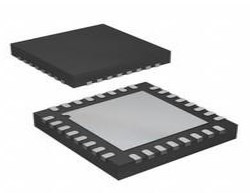
Tape & Reel (TR) ±20V 60V 8-PowerVDFN
The CSD18543Q3A is a 60-V N-Channel NexFET™ Power MOSFET. This article mainly introduces Features, Pinout, Datasheet and other detailed information about Texas Instruments CSD18543Q3A.

Power MOSFET working, structure and characteristics in Power Electronics by Engineering Funda
CSD18543Q3A Description
The CSD18543Q3A is a 60-V, 8.1-m, SON 3.3-mm 3.3-mm NexFETTM power MOSFET designed to reduce losses in power conversion applications.
CSD18543Q3A Pinout

CSD18543Q3A CAD Model


CSD18543Q3A Features
• Ultra-Low Qg and Qgd
• Low RDS(on)
• Low-Thermal Resistance
• Avalanche Rated
• Lead Free
• Halogen Free
• SON 3.3-mm × 3.3-mm Plastic Package
Specifications
- TypeParameter
- Lifecycle Status
Lifecycle Status refers to the current stage of an electronic component in its product life cycle, indicating whether it is active, obsolete, or transitioning between these states. An active status means the component is in production and available for purchase. An obsolete status indicates that the component is no longer being manufactured or supported, and manufacturers typically provide a limited time frame for support. Understanding the lifecycle status is crucial for design engineers to ensure continuity and reliability in their projects.
ACTIVE (Last Updated: 4 days ago) - Factory Lead Time12 Weeks
- Mounting Type
The "Mounting Type" in electronic components refers to the method used to attach or connect a component to a circuit board or other substrate, such as through-hole, surface-mount, or panel mount.
Surface Mount - Package / Case
refers to the protective housing that encases an electronic component, providing mechanical support, electrical connections, and thermal management.
8-PowerVDFN - Surface Mount
having leads that are designed to be soldered on the side of a circuit board that the body of the component is mounted on.
YES - Number of Pins8
- Drive Voltage (Max Rds On, Min Rds On)4.5V 10V
- Number of Elements1
- Turn Off Delay Time
It is the time from when Vgs drops below 90% of the gate drive voltage to when the drain current drops below 90% of the load current. It is the delay before current starts to transition in the load, and depends on Rg. Ciss.
8 ns - Packaging
Semiconductor package is a carrier / shell used to contain and cover one or more semiconductor components or integrated circuits. The material of the shell can be metal, plastic, glass or ceramic.
Tape & Reel (TR) - JESD-609 Code
The "JESD-609 Code" in electronic components refers to a standardized marking code that indicates the lead-free solder composition and finish of electronic components for compliance with environmental regulations.
e3 - Pbfree Code
The "Pbfree Code" parameter in electronic components refers to the code or marking used to indicate that the component is lead-free. Lead (Pb) is a toxic substance that has been widely used in electronic components for many years, but due to environmental concerns, there has been a shift towards lead-free alternatives. The Pbfree Code helps manufacturers and users easily identify components that do not contain lead, ensuring compliance with regulations and promoting environmentally friendly practices. It is important to pay attention to the Pbfree Code when selecting electronic components to ensure they meet the necessary requirements for lead-free applications.
yes - Part Status
Parts can have many statuses as they progress through the configuration, analysis, review, and approval stages.
Active - Moisture Sensitivity Level (MSL)
Moisture Sensitivity Level (MSL) is a standardized rating that indicates the susceptibility of electronic components, particularly semiconductors, to moisture-induced damage during storage and the soldering process, defining the allowable exposure time to ambient conditions before they require special handling or baking to prevent failures
1 (Unlimited) - Number of Terminations5
- ECCN Code
An ECCN (Export Control Classification Number) is an alphanumeric code used by the U.S. Bureau of Industry and Security to identify and categorize electronic components and other dual-use items that may require an export license based on their technical characteristics and potential for military use.
EAR99 - Terminal Finish
Terminal Finish refers to the surface treatment applied to the terminals or leads of electronic components to enhance their performance and longevity. It can improve solderability, corrosion resistance, and overall reliability of the connection in electronic assemblies. Common finishes include nickel, gold, and tin, each possessing distinct properties suitable for various applications. The choice of terminal finish can significantly impact the durability and effectiveness of electronic devices.
Matte Tin (Sn) - Max Operating Temperature
The Maximum Operating Temperature is the maximum body temperature at which the thermistor is designed to operate for extended periods of time with acceptable stability of its electrical characteristics.
150°C - Min Operating Temperature
The "Min Operating Temperature" parameter in electronic components refers to the lowest temperature at which the component is designed to operate effectively and reliably. This parameter is crucial for ensuring the proper functioning and longevity of the component, as operating below this temperature may lead to performance issues or even damage. Manufacturers specify the minimum operating temperature to provide guidance to users on the environmental conditions in which the component can safely operate. It is important to adhere to this parameter to prevent malfunctions and ensure the overall reliability of the electronic system.
-55°C - Additional Feature
Any Feature, including a modified Existing Feature, that is not an Existing Feature.
AVALANCHE RATED - Terminal Position
In electronic components, the term "Terminal Position" refers to the physical location of the connection points on the component where external electrical connections can be made. These connection points, known as terminals, are typically used to attach wires, leads, or other components to the main body of the electronic component. The terminal position is important for ensuring proper connectivity and functionality of the component within a circuit. It is often specified in technical datasheets or component specifications to help designers and engineers understand how to properly integrate the component into their circuit designs.
DUAL - Terminal Form
Occurring at or forming the end of a series, succession, or the like; closing; concluding.
FLAT - Base Part Number
The "Base Part Number" (BPN) in electronic components serves a similar purpose to the "Base Product Number." It refers to the primary identifier for a component that captures the essential characteristics shared by a group of similar components. The BPN provides a fundamental way to reference a family or series of components without specifying all the variations and specific details.
CSD18543 - Number of Channels1
- Element Configuration
The distribution of electrons of an atom or molecule (or other physical structure) in atomic or molecular orbitals.
Single - Operating Mode
A phase of operation during the operation and maintenance stages of the life cycle of a facility.
ENHANCEMENT MODE - Power Dissipation
the process by which an electronic or electrical device produces heat (energy loss or waste) as an undesirable derivative of its primary action.
66W - Case Connection
Case Connection refers to the method by which an electronic component's case or housing is connected to the electrical circuit. This connection is important for grounding purposes, mechanical stability, and heat dissipation. The case connection can vary depending on the type of component and its intended application. It is crucial to ensure a secure and reliable case connection to maintain the overall performance and safety of the electronic device.
DRAIN - Turn On Delay Time
Turn-on delay, td(on), is the time taken to charge the input capacitance of the device before drain current conduction can start.
9 ns - Transistor Application
In the context of electronic components, the parameter "Transistor Application" refers to the specific purpose or function for which a transistor is designed and used. Transistors are semiconductor devices that can amplify or switch electronic signals and are commonly used in various electronic circuits. The application of a transistor can vary widely depending on its design and characteristics, such as whether it is intended for audio amplification, digital logic, power control, or radio frequency applications. Understanding the transistor application is important for selecting the right type of transistor for a particular circuit or system to ensure optimal performance and functionality.
SWITCHING - Drain to Source Voltage (Vdss)
The Drain to Source Voltage (Vdss) is a key parameter in electronic components, particularly in field-effect transistors (FETs) such as MOSFETs. It refers to the maximum voltage that can be applied between the drain and source terminals of the FET without causing damage to the component. Exceeding this voltage limit can lead to breakdown and potentially permanent damage to the device.Vdss is an important specification to consider when designing or selecting components for a circuit, as it determines the operating range and reliability of the FET. It is crucial to ensure that the Vdss rating of the component is higher than the maximum voltage expected in the circuit to prevent failures and ensure proper functionality.In summary, the Drain to Source Voltage (Vdss) is a critical parameter that defines the maximum voltage tolerance of a FET component and plays a significant role in determining the overall performance and reliability of electronic circuits.
60V - Vgs (Max)
Vgs (Max) refers to the maximum gate-source voltage that can be applied to a field-effect transistor (FET) without causing damage to the component. This parameter is crucial in determining the safe operating limits of the FET and helps prevent overvoltage conditions that could lead to device failure. Exceeding the specified Vgs (Max) rating can result in breakdown of the gate oxide layer, leading to permanent damage to the FET. Designers must ensure that the applied gate-source voltage does not exceed the maximum rating to ensure reliable and long-term operation of the electronic component.
±20V - Polarity/Channel Type
In electronic components, the parameter "Polarity/Channel Type" refers to the characteristic that determines the direction of current flow or the type of signal that can be accommodated by the component. For components like diodes and transistors, polarity indicates the direction in which current can flow through the component, such as forward bias or reverse bias for diodes. For components like MOSFETs or JFETs, the channel type refers to whether the component is an N-channel or P-channel device, which determines the type of charge carriers that carry current through the component. Understanding the polarity or channel type of a component is crucial for proper circuit design and ensuring that the component is connected correctly to achieve the desired functionality.
N-CHANNEL - Continuous Drain Current (ID)
Continuous Drain Current (ID) is a key parameter in electronic components, particularly in field-effect transistors (FETs) such as MOSFETs. It refers to the maximum current that can flow continuously through the drain terminal of the FET without causing damage to the component. This parameter is crucial for determining the power handling capability of the FET and is specified by the manufacturer in the component's datasheet. Designers must ensure that the actual operating current does not exceed the specified Continuous Drain Current to prevent overheating and potential failure of the component.
35A - Gate to Source Voltage (Vgs)
The Gate to Source Voltage (Vgs) is a crucial parameter in electronic components, particularly in field-effect transistors (FETs) such as MOSFETs. It refers to the voltage difference between the gate and source terminals of the FET. This voltage determines the conductivity of the FET and controls the flow of current through the device. By varying the Vgs, the FET can be switched on or off, allowing for precise control of electronic circuits. Understanding and properly managing the Vgs is essential for ensuring the reliable and efficient operation of FET-based circuits.
20V - Avalanche Energy Rating (Eas)
Avalanche Energy Rating (Eas) is a parameter that quantifies the energy handling capability of a semiconductor device, particularly during avalanche breakdown conditions. It indicates the maximum energy that the device can withstand without being damaged when it experiences an avalanche effect. This rating is crucial for applications where devices might be exposed to over-voltage or other conditions that could cause unintended breakdown, ensuring reliability and longevity in operation. The Eas value helps designers select appropriate components for circuits that may encounter transient events.
55 mJ - FET Technology
Field-Effect Transistor (FET) technology is a type of semiconductor device commonly used in electronic components such as transistors and integrated circuits. FETs operate by controlling the flow of current through a semiconductor channel using an electric field. There are several types of FETs, including Metal-Oxide-Semiconductor FETs (MOSFETs) and Junction FETs (JFETs), each with its own characteristics and applications. FET technology offers advantages such as high input impedance, low power consumption, and fast switching speeds, making it suitable for a wide range of electronic devices and circuits. Overall, FET technology plays a crucial role in modern electronics by enabling efficient and reliable signal processing and amplification.
METAL-OXIDE SEMICONDUCTOR - Max Junction Temperature (Tj)
Max Junction Temperature (Tj) refers to the maximum allowable temperature at the junction of a semiconductor device, such as a transistor or integrated circuit. It is a critical parameter that influences the performance, reliability, and lifespan of the component. Exceeding this temperature can lead to thermal runaway, breakdown, or permanent damage to the device. Proper thermal management is essential to ensure the junction temperature remains within safe operating limits during device operation.
150°C - Drain to Source Resistance
The Drain to Source Resistance, often denoted as RDS(on), is a crucial parameter in electronic components, particularly in field-effect transistors (FETs) such as MOSFETs. It represents the resistance between the drain and source terminals when the FET is in its on-state, conducting current. A lower RDS(on) value indicates better conductivity and efficiency, as it results in less power dissipation and heat generation in the component. Designers often aim to minimize RDS(on) to improve the performance and overall efficiency of electronic circuits, especially in power applications where minimizing losses is critical.
8.1mOhm - Feedback Cap-Max (Crss)
Feedback Cap-Max (Crss) refers to the maximum capacitance between the output and input of an electronic component, such as a transistor or an operational amplifier. It indicates the level of feedback capacitance that can negatively affect the performance, stability, and bandwidth of the device. A higher Crss value may introduce unintended phase shifts or frequency response issues, making it crucial to consider in circuit design to ensure optimal operation.
6.2 pF - Height900μm
- Length3.3mm
- Width3.3mm
- Thickness
Thickness in electronic components refers to the measurement of how thick a particular material or layer is within the component structure. It can pertain to various aspects, such as the thickness of a substrate, a dielectric layer, or conductive traces. This parameter is crucial as it impacts the electrical, mechanical, and thermal properties of the component, influencing its performance and reliability in electronic circuits.
800μm - RoHS Status
RoHS means “Restriction of Certain Hazardous Substances” in the “Hazardous Substances Directive” in electrical and electronic equipment.
ROHS3 Compliant
CSD18543Q3A Alternatives
| Part Number | Description | Manufacturer |
| NTMFS5844NLT3GTRANSISTORS | 11A, 60V, 0.015ohm, N-CHANNEL, Si, POWER, MOSFET, HALOGEN FREE AND ROHS COMPLIANT, CASE 488AA-01, DFN5, SOP-8 | onsemi |
| TSM120N06LCPROGTRANSISTORS | Power Field-Effect Transistor, 10A I(D), 60V, 0.015ohm, 1-Element, N-Channel, Silicon, Metal-oxide Semiconductor FET, TO-252, DPAK-3/2 | Taiwan Semiconductor |
| NVTFS5C673NLWFTAGTRANSISTORS | Single N-Channel Power MOSFET 60V, 50A, 9.8mΩ 1500 / Tape & Reel. Pb-Free, Wettable Flanks, 1500-REEL | onsemi |
| NVTFS5820NLWFTWGTRANSISTORS | Power MOSFET 60V, 29A, 11.5 mOhm, Single N-Channel, u8FL, Logic Level., WDFN8 3.3x3.3, 0.65P, 5000-REEL | onsemi |
| NVTFS5820NLT1GTRANSISTORS | 11A, 60V, 0.015ohm, N-CHANNEL, Si, POWER, MOSFET, LEAD FREE, CASE 511AB-01, WDFN-8 | onsemi |
| NTMFS5844NLT1GTRANSISTORS | Single N-Channel Power MOSFET 60V, 60A, 12mΩ Power MOSFET 60V 60A 12mOhm Single N-Channel SO-8FL, DFN5 5X6, 1.27P (SO 8FL), 1500-REEL | onsemi |
| NVTFS5C673NLTAGTRANSISTORS | Single N-Channel Power MOSFET 60V, 50A, 9.8mΩ 1500 / Tape & Reel, 1500-REEL | onsemi |
| NVTFS5820NLT3GTRANSISTORS | 11A, 60V, 0.015ohm, N-CHANNEL, Si, POWER, MOSFET, LEAD FREE, CASE 511AB-01, WDFN-8 | onsemi |
| NVTFS5820NLTWGTRANSISTORS | Power MOSFET 60V, 29A, 11.5 mOhm, Single N-Channel, u8FL, Logic Level., WDFN8 3.3x3.3, 0.65P, 5000-REEL | onsemi |
CSD18543Q3A Applications
• Solid State Relay Switch
• DC-DC Conversion
• Secondary Side Synchronous Rectifier
• Isolated Converter Primary Side Switch
• Motor Control
CSD18543Q3A Package

CSD18543Q3A Manufacturer
As a global semiconductor company operating in 35 countries, Texas Instruments (TI) is first and foremost a reflection of its people. From the TIer who unveiled the first working integrated circuit in 1958 to the more than 30,000 TIers around the world today who design, manufacture and sell analog and embedded processing chips, we are problem-solvers collaborating to change the world through technology.
Trend Analysis
What is a power MOSFET used for?
A type of metal oxide semiconductor field-effect transistor (MOSFET) is used to switch large amounts of current. Power MOSFETs use a vertical structure with source and drain terminals at opposite sides of the chip. The vertical orientation eliminates crowding at the gate and offers larger channel widths.
What is the difference between MOSFET and power MOSFET?
Normal MOSFET handles low power but power MOSFET can handle much higher power. Power MOSFET is used in Power Electronics.
What are the advantages of power MOSFET?
Ability to scale down in size.
It has low power consumption to allow more components per chip surface area.
MOSFET has no gate diode.
It read directly with a very thin active area.
They have high drain resistance due to the lower resistance of a channel.
 A Comprehensive Guide to LTC7821IUH#PBF DC-DC Switching Controller
06 March 2024254
 FT232R USB UART IC: Features, Pinout and Datasheet
10 February 202229449
 ADF4351 Synthesizer: Datasheet, Pinout and Alternatives
24 August 202110724
 SN74HC164N: Features, Applications, and Datasheet
07 December 20232935
 What you need to know about TPA3110 Bluetooth Audio Power Amplifier Board
26 April 202218625
 BF494 Transistor: Circuits, Pinout, and Datasheet
30 December 202112164
 AD8479 Precision Difference Amplifier: Pinout and Basic Connections
12 November 20211925
 Introduction to NXP KL28Z Microcontroller
28 February 2024222
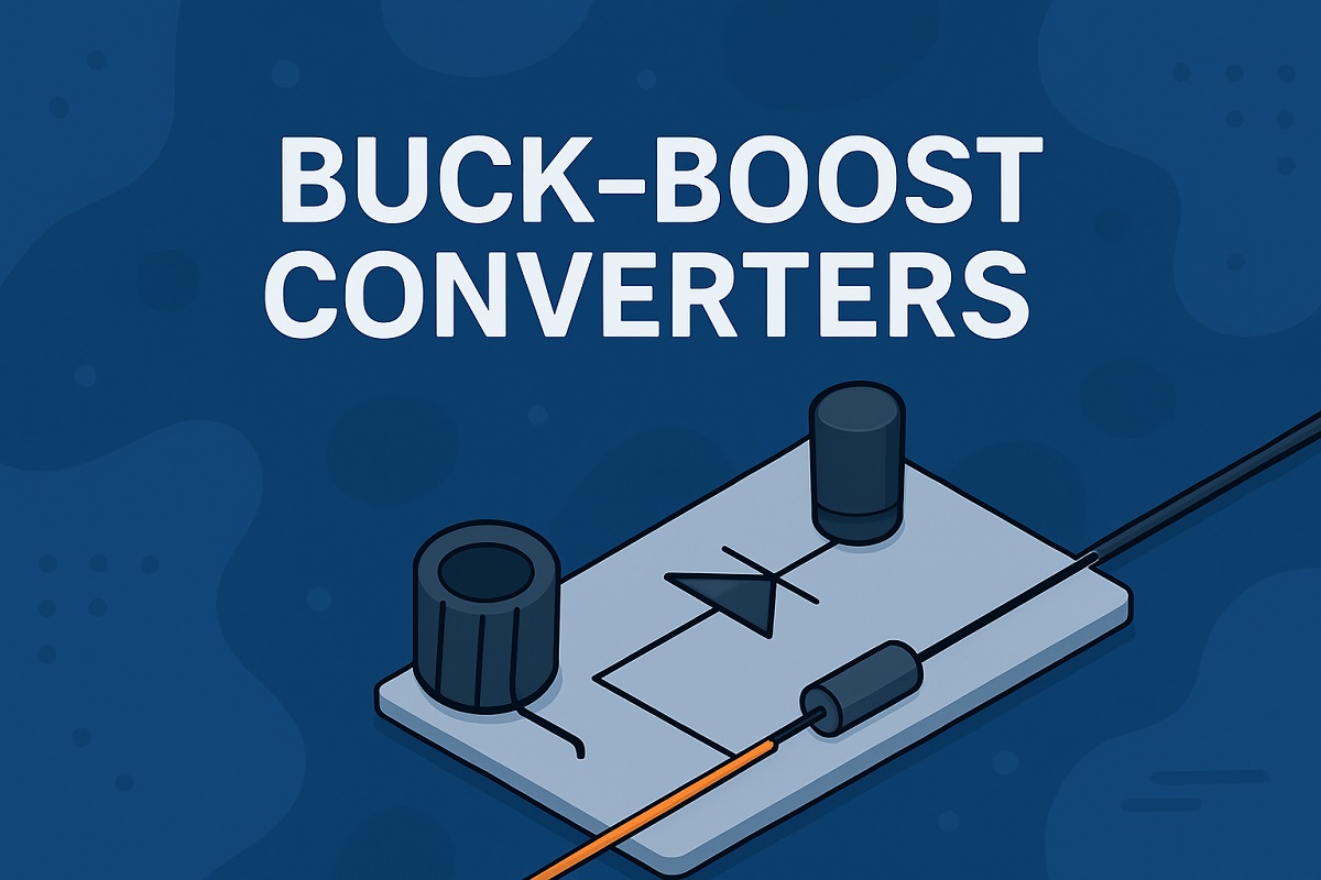 What Are Buck-Boost Converters?
07 June 20251118
 What is a Reed Relay?
16 April 20219387
 Linear Induction Motor: Working Principle, Characteristics, and Applications
02 March 202115728
 Role of Solar Energy in Wide-Band Gap Devices for Photovoltaic Applications
15 March 20244616
 CCTC Authorized Distributor | UTMEL Electronics
22 February 20257687
 Network Interface Card: Types, Functions and Buying Guide
17 August 202110723
 What causes the Noise of Electronic Equipment when it is Running?
01 August 20222918
 Introduction to Semiconductor Devices
17 October 202515563
Texas Instruments
In Stock: 1633
United States
China
Canada
Japan
Russia
Germany
United Kingdom
Singapore
Italy
Hong Kong(China)
Taiwan(China)
France
Korea
Mexico
Netherlands
Malaysia
Austria
Spain
Switzerland
Poland
Thailand
Vietnam
India
United Arab Emirates
Afghanistan
Åland Islands
Albania
Algeria
American Samoa
Andorra
Angola
Anguilla
Antigua & Barbuda
Argentina
Armenia
Aruba
Australia
Azerbaijan
Bahamas
Bahrain
Bangladesh
Barbados
Belarus
Belgium
Belize
Benin
Bermuda
Bhutan
Bolivia
Bonaire, Sint Eustatius and Saba
Bosnia & Herzegovina
Botswana
Brazil
British Indian Ocean Territory
British Virgin Islands
Brunei
Bulgaria
Burkina Faso
Burundi
Cabo Verde
Cambodia
Cameroon
Cayman Islands
Central African Republic
Chad
Chile
Christmas Island
Cocos (Keeling) Islands
Colombia
Comoros
Congo
Congo (DRC)
Cook Islands
Costa Rica
Côte d’Ivoire
Croatia
Cuba
Curaçao
Cyprus
Czechia
Denmark
Djibouti
Dominica
Dominican Republic
Ecuador
Egypt
El Salvador
Equatorial Guinea
Eritrea
Estonia
Eswatini
Ethiopia
Falkland Islands
Faroe Islands
Fiji
Finland
French Guiana
French Polynesia
Gabon
Gambia
Georgia
Ghana
Gibraltar
Greece
Greenland
Grenada
Guadeloupe
Guam
Guatemala
Guernsey
Guinea
Guinea-Bissau
Guyana
Haiti
Honduras
Hungary
Iceland
Indonesia
Iran
Iraq
Ireland
Isle of Man
Israel
Jamaica
Jersey
Jordan
Kazakhstan
Kenya
Kiribati
Kosovo
Kuwait
Kyrgyzstan
Laos
Latvia
Lebanon
Lesotho
Liberia
Libya
Liechtenstein
Lithuania
Luxembourg
Macao(China)
Madagascar
Malawi
Maldives
Mali
Malta
Marshall Islands
Martinique
Mauritania
Mauritius
Mayotte
Micronesia
Moldova
Monaco
Mongolia
Montenegro
Montserrat
Morocco
Mozambique
Myanmar
Namibia
Nauru
Nepal
New Caledonia
New Zealand
Nicaragua
Niger
Nigeria
Niue
Norfolk Island
North Korea
North Macedonia
Northern Mariana Islands
Norway
Oman
Pakistan
Palau
Palestinian Authority
Panama
Papua New Guinea
Paraguay
Peru
Philippines
Pitcairn Islands
Portugal
Puerto Rico
Qatar
Réunion
Romania
Rwanda
Samoa
San Marino
São Tomé & Príncipe
Saudi Arabia
Senegal
Serbia
Seychelles
Sierra Leone
Sint Maarten
Slovakia
Slovenia
Solomon Islands
Somalia
South Africa
South Sudan
Sri Lanka
St Helena, Ascension, Tristan da Cunha
St. Barthélemy
St. Kitts & Nevis
St. Lucia
St. Martin
St. Pierre & Miquelon
St. Vincent & Grenadines
Sudan
Suriname
Svalbard & Jan Mayen
Sweden
Syria
Tajikistan
Tanzania
Timor-Leste
Togo
Tokelau
Tonga
Trinidad & Tobago
Tunisia
Turkey
Turkmenistan
Turks & Caicos Islands
Tuvalu
U.S. Outlying Islands
U.S. Virgin Islands
Uganda
Ukraine
Uruguay
Uzbekistan
Vanuatu
Vatican City
Venezuela
Wallis & Futuna
Yemen
Zambia
Zimbabwe
![CSD25303W1015]() CSD25303W1015
CSD25303W1015Texas Instruments
![CSD18531Q5A]() CSD18531Q5A
CSD18531Q5ATexas Instruments
![CSD25402Q3A]() CSD25402Q3A
CSD25402Q3ATexas Instruments
![CSD18532Q5B]() CSD18532Q5B
CSD18532Q5BTexas Instruments
![CSD16301Q2]() CSD16301Q2
CSD16301Q2Texas Instruments
![CSD17313Q2]() CSD17313Q2
CSD17313Q2Texas Instruments
![CSD16406Q3]() CSD16406Q3
CSD16406Q3Texas Instruments
![CSD18504Q5A]() CSD18504Q5A
CSD18504Q5ATexas Instruments
![CSD19532Q5B]() CSD19532Q5B
CSD19532Q5BTexas Instruments


