
 Product
 Brand
Brand Articles
 Tools
Tools
INA115BU Instrumentation Amplifier:Datasheet, Application, Circuit

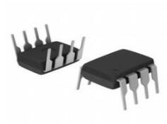
20mA per Channel 500pA 110 dB Instrumentational OP Amps 0.002μA 4.5V~36V ±2.25V~18V INA115 16 Pins 16-SOIC (0.295, 7.50mm Width)


20mA per Channel 500pA 110 dB Instrumentational OP Amps 0.002μA 4.5V~36V ±2.25V~18V INA115 16 Pins 16-SOIC (0.295, 7.50mm Width)
This article will unlock more details about INA115BU, a low cost, general purpose instrumentation amplifier.
INA115BU Pinout

INA115BU Pinout
INA115BU CAD Model
Symbol

INA115BU Symbol
Footprint

INA115BU Footprint
3D Model

INA115BU 3D Model
INA115BU Description
The INA115BU is a low cost, general-purpose instrumentation amplifier offering excellent accuracy. Its versatile three-op amp design and small size make it ideal for a wide range of applications. Similar to the model INA114, the INA115BU provides additional connections to the input op-amps, A1 and A2, which improve gain accuracy in high gains and are useful in forming switched-gain amplifiers.
Specifications
- TypeParameter
- Factory Lead Time6 Weeks
- Mounting Type
The "Mounting Type" in electronic components refers to the method used to attach or connect a component to a circuit board or other substrate, such as through-hole, surface-mount, or panel mount.
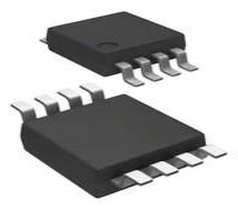
Surface Mount - Package / Case
refers to the protective housing that encases an electronic component, providing mechanical support, electrical connections, and thermal management.
16-SOIC (0.295, 7.50mm Width) - Surface Mount
having leads that are designed to be soldered on the side of a circuit board that the body of the component is mounted on.
YES - Number of Pins16
- Weight420.395078mg
- Number of Elements3
- Operating Temperature
The operating temperature is the range of ambient temperature within which a power supply, or any other electrical equipment, operate in. This ranges from a minimum operating temperature, to a peak or maximum operating temperature, outside which, the power supply may fail.
-40°C~85°C - Packaging
Semiconductor package is a carrier / shell used to contain and cover one or more semiconductor components or integrated circuits. The material of the shell can be metal, plastic, glass or ceramic.
Tube - JESD-609 Code
The "JESD-609 Code" in electronic components refers to a standardized marking code that indicates the lead-free solder composition and finish of electronic components for compliance with environmental regulations.
e4 - Part Status
Parts can have many statuses as they progress through the configuration, analysis, review, and approval stages.
Active - Moisture Sensitivity Level (MSL)
Moisture Sensitivity Level (MSL) is a standardized rating that indicates the susceptibility of electronic components, particularly semiconductors, to moisture-induced damage during storage and the soldering process, defining the allowable exposure time to ambient conditions before they require special handling or baking to prevent failures
3 (168 Hours) - Number of Terminations16
- ECCN Code
An ECCN (Export Control Classification Number) is an alphanumeric code used by the U.S. Bureau of Industry and Security to identify and categorize electronic components and other dual-use items that may require an export license based on their technical characteristics and potential for military use.
EAR99 - Resistance
Resistance is a fundamental property of electronic components that measures their opposition to the flow of electric current. It is denoted by the symbol "R" and is measured in ohms (Ω). Resistance is caused by the collisions of electrons with atoms in a material, which generates heat and reduces the flow of current. Components with higher resistance will impede the flow of current more than those with lower resistance. Resistance plays a crucial role in determining the behavior and functionality of electronic circuits, such as limiting current flow, voltage division, and controlling power dissipation.
10GOhm - Terminal Finish
Terminal Finish refers to the surface treatment applied to the terminals or leads of electronic components to enhance their performance and longevity. It can improve solderability, corrosion resistance, and overall reliability of the connection in electronic assemblies. Common finishes include nickel, gold, and tin, each possessing distinct properties suitable for various applications. The choice of terminal finish can significantly impact the durability and effectiveness of electronic devices.
Nickel/Palladium/Gold (Ni/Pd/Au) - Terminal Position
In electronic components, the term "Terminal Position" refers to the physical location of the connection points on the component where external electrical connections can be made. These connection points, known as terminals, are typically used to attach wires, leads, or other components to the main body of the electronic component. The terminal position is important for ensuring proper connectivity and functionality of the component within a circuit. It is often specified in technical datasheets or component specifications to help designers and engineers understand how to properly integrate the component into their circuit designs.
DUAL - Terminal Form
Occurring at or forming the end of a series, succession, or the like; closing; concluding.
GULL WING - Peak Reflow Temperature (Cel)
Peak Reflow Temperature (Cel) is a parameter that specifies the maximum temperature at which an electronic component can be exposed during the reflow soldering process. Reflow soldering is a common method used to attach electronic components to a circuit board. The Peak Reflow Temperature is crucial because it ensures that the component is not damaged or degraded during the soldering process. Exceeding the specified Peak Reflow Temperature can lead to issues such as component failure, reduced performance, or even permanent damage to the component. It is important for manufacturers and assemblers to adhere to the recommended Peak Reflow Temperature to ensure the reliability and functionality of the electronic components.
260 - Number of Functions1
- Supply Voltage
Supply voltage refers to the electrical potential difference provided to an electronic component or circuit. It is crucial for the proper operation of devices, as it powers their functions and determines performance characteristics. The supply voltage must be within specified limits to ensure reliability and prevent damage to components. Different electronic devices have specific supply voltage requirements, which can vary widely depending on their design and intended application.
15V - Time@Peak Reflow Temperature-Max (s)
Time@Peak Reflow Temperature-Max (s) refers to the maximum duration that an electronic component can be exposed to the peak reflow temperature during the soldering process, which is crucial for ensuring reliable solder joint formation without damaging the component.
NOT SPECIFIED - Base Part Number
The "Base Part Number" (BPN) in electronic components serves a similar purpose to the "Base Product Number." It refers to the primary identifier for a component that captures the essential characteristics shared by a group of similar components. The BPN provides a fundamental way to reference a family or series of components without specifying all the variations and specific details.
INA115 - Pin Count
a count of all of the component leads (or pins)
16 - Qualification Status
An indicator of formal certification of qualifications.
Not Qualified - Number of Circuits1
- Operating Supply Current
Operating Supply Current, also known as supply current or quiescent current, is a crucial parameter in electronic components that indicates the amount of current required for the device to operate under normal conditions. It represents the current drawn by the component from the power supply while it is functioning. This parameter is important for determining the power consumption of the component and is typically specified in datasheets to help designers calculate the overall power requirements of their circuits. Understanding the operating supply current is essential for ensuring proper functionality and efficiency of electronic systems.
2.2mA - Nominal Supply Current
Nominal current is the same as the rated current. It is the current drawn by the motor while delivering rated mechanical output at its shaft.
3mA - Max Supply Current
Max Supply Current refers to the maximum amount of electrical current that a component can draw from its power supply under normal operating conditions. It is a critical parameter that ensures the component operates reliably without exceeding its thermal limits or damaging internal circuitry. Exceeding this current can lead to overheating, performance degradation, or failure of the component. Understanding this parameter is essential for designing circuits that provide adequate power while avoiding overload situations.
3mA - Quiescent Current
The quiescent current is defined as the current level in the amplifier when it is producing an output of zero.
2.2mA - Slew Rate
the maximum rate of output voltage change per unit time.
0.6V/μs - Amplifier Type
Amplifier Type refers to the classification or categorization of amplifiers based on their design, functionality, and characteristics. Amplifiers are electronic devices that increase the amplitude of a signal, such as voltage or current. The type of amplifier determines its specific application, performance capabilities, and operating characteristics. Common types of amplifiers include operational amplifiers (op-amps), power amplifiers, audio amplifiers, and radio frequency (RF) amplifiers. Understanding the amplifier type is crucial for selecting the right component for a particular circuit or system design.
Instrumentation - Common Mode Rejection Ratio
Common Mode Rejection Ratio (CMRR) is a measure of the ability of a differential amplifier to reject input signals that are common to both input terminals. It is defined as the ratio of the differential gain to the common mode gain. A high CMRR indicates that the amplifier can effectively eliminate noise and interference that affects both inputs simultaneously, enhancing the fidelity of the amplified signal. CMRR is typically expressed in decibels (dB), with higher values representing better performance in rejecting common mode signals.
110 dB - Current - Input Bias
The parameter "Current - Input Bias" in electronic components refers to the amount of current required at the input terminal of a device to maintain proper operation. It is a crucial specification as it determines the minimum input current needed for the component to function correctly. Input bias current can affect the performance and accuracy of the device, especially in precision applications where small signal levels are involved. It is typically specified in datasheets for operational amplifiers, transistors, and other semiconductor devices to provide users with important information for circuit design and analysis.
500pA - Voltage - Supply, Single/Dual (±)
The parameter "Voltage - Supply, Single/Dual (±)" in electronic components refers to the power supply voltage required for the proper operation of the component. This parameter indicates whether the component requires a single power supply voltage (e.g., 5V) or a dual power supply voltage (e.g., ±15V). For components that require a single power supply voltage, only one voltage level is needed for operation. On the other hand, components that require a dual power supply voltage need both positive and negative voltage levels to function correctly.Understanding the voltage supply requirements of electronic components is crucial for designing and integrating them into circuits to ensure proper functionality and prevent damage due to incorrect voltage levels.
4.5V~36V ±2.25V~18V - Output Current per Channel
Output Current per Channel is a specification commonly found in electronic components such as amplifiers, audio interfaces, and power supplies. It refers to the maximum amount of electrical current that can be delivered by each individual output channel of the component. This parameter is important because it determines the capacity of the component to drive connected devices or loads. A higher output current per channel means the component can deliver more power to connected devices, while a lower output current may limit the performance or functionality of the component in certain applications. It is crucial to consider the output current per channel when selecting electronic components to ensure they can meet the power requirements of the intended system or setup.
20mA - Input Offset Voltage (Vos)
Input Offset Voltage (Vos) is a key parameter in electronic components, particularly in operational amplifiers. It refers to the voltage difference that must be applied between the two input terminals of the amplifier to nullify the output voltage when the input terminals are shorted together. In simpler terms, it represents the voltage required to bring the output of the amplifier to zero when there is no input signal present. Vos is an important parameter as it can introduce errors in the output signal of the amplifier, especially in precision applications where accuracy is crucial. Minimizing Vos is essential to ensure the amplifier operates with high precision and accuracy.
10μV - Neg Supply Voltage-Nom (Vsup)
The parameter "Neg Supply Voltage-Nom (Vsup)" in electronic components refers to the nominal negative supply voltage that the component requires to operate within its specified performance characteristics. This parameter indicates the minimum voltage level that must be provided to the component's negative supply pin for proper functionality. It is important to ensure that the negative supply voltage provided to the component does not exceed the maximum specified value to prevent damage or malfunction. Understanding and adhering to the specified negative supply voltage requirements is crucial for the reliable operation of the electronic component in a circuit.
-15V - Voltage Gain
Voltage gain is a measure of how much an electronic component or circuit amplifies an input voltage signal to produce an output voltage signal. It is typically expressed as a ratio or in decibels (dB). A higher voltage gain indicates a greater amplification of the input signal. Voltage gain is an important parameter in amplifiers, where it determines the level of amplification provided by the circuit. It is calculated by dividing the output voltage by the input voltage and is a key factor in determining the overall performance and functionality of electronic devices.
80dB - Average Bias Current-Max (IIB)
The parameter "Average Bias Current-Max (IIB)" in electronic components refers to the maximum average bias current that the component can handle without exceeding its specified operating limits. Bias current is the current that flows through a component when it is in its quiescent state or when it is not actively processing a signal. Exceeding the maximum average bias current can lead to overheating, reduced performance, or even damage to the component. Therefore, it is important to ensure that the bias current does not exceed the specified maximum value to maintain the reliability and longevity of the electronic component.
0.002μA - -3db Bandwidth
The "-3dB bandwidth" of an electronic component refers to the frequency range over which the component's output signal power is reduced by 3 decibels (dB) compared to its maximum output power. This parameter is commonly used to describe the frequency response of components such as amplifiers, filters, and other signal processing devices. The -3dB point is significant because it represents the half-power point, where the output signal power is reduced to half of its maximum value. Understanding the -3dB bandwidth is important for designing and analyzing electronic circuits to ensure that signals are accurately processed within the desired frequency range.
1MHz - Dual Supply Voltage
Dual Supply Voltage refers to an electronic component's requirement for two separate power supply voltages, typically one positive and one negative. This configuration is commonly used in operational amplifiers, analog circuits, and certain digital devices to allow for greater signal handling capabilities and improved performance. The use of dual supply voltages enables the device to process bipolar signals, thereby enhancing its functionality in various applications.
15V - Input Offset Current-Max (IIO)
Input Offset Current-Max (IIO) is a parameter that describes the maximum difference in input bias currents between two input terminals of an electronic component, such as an operational amplifier. Input offset current can cause errors in the output of the component, especially in precision applications where accuracy is crucial. The IIO specification provides a limit on the maximum allowable difference in input currents to ensure that the component operates within its specified performance range. Designers need to consider the IIO value when selecting components and designing circuits to minimize errors and ensure reliable operation.
0.002μA - Input Voltage Noise Density
Input Voltage Noise Density refers to the measure of noise voltage present at the input of an electronic component, typically expressed in volts per square root hertz (V/√Hz). It characterizes the amount of noise introduced by the component, independent of the signal level. This parameter is crucial for understanding the overall performance of amplifiers, sensors, and other devices, as it impacts the signal-to-noise ratio and limits the achievable resolution and sensitivity in electronic systems. Lower values of input voltage noise density indicate better performance in terms of noise characteristics.
11nV/sqrt Hz - Voltage Gain-Nom
Voltage Gain-Nom is a parameter used to describe the ratio of the output voltage to the input voltage in electronic components such as amplifiers. It represents the amplification factor of the component and indicates how much the input voltage is amplified to produce the output voltage. The "Nom" in the term signifies that this value is the nominal or typical voltage gain under specified operating conditions. A higher voltage gain indicates a greater amplification of the input signal, while a lower voltage gain signifies less amplification. This parameter is crucial in determining the performance and functionality of electronic circuits and devices.
10 - Height2.35mm
- Length10.28mm
- Width7.52mm
- RoHS Status
RoHS means “Restriction of Certain Hazardous Substances” in the “Hazardous Substances Directive” in electrical and electronic equipment.
ROHS3 Compliant - Lead Free
Lead Free is a term used to describe electronic components that do not contain lead as part of their composition. Lead is a toxic material that can have harmful effects on human health and the environment, so the electronics industry has been moving towards lead-free components to reduce these risks. Lead-free components are typically made using alternative materials such as silver, copper, and tin. Manufacturers must comply with regulations such as the Restriction of Hazardous Substances (RoHS) directive to ensure that their products are lead-free and environmentally friendly.
Lead Free
Parts with Similar Specs
- ImagePart NumberManufacturerPackage / CaseNumber of PinsNumber of CircuitsSlew RateInput Offset Voltage (Vos)Common Mode Rejection RatioSupply VoltageOperating Supply CurrentView Compare
![INA115BUG4]()
INA115BUG4
16-SOIC (0.295, 7.50mm Width)
16
1
0.6V/μs
10 μV
110 dB
15 V
2.2 mA
![INA115AU]()
16-SOIC (0.295, 7.50mm Width)
16
-
0.6V/μs
125 μV
106 dB
15 V
2.2 mA
![INA115BU]()
16-SOIC (0.295, 7.50mm Width)
16
-
0.6V/μs
50 μV
110 dB
15 V
2.2 mA
![INA114AU]()
16-SOIC (0.295, 7.50mm Width)
16
-
0.6V/μs
125 μV
106 dB
15 V
2.2 mA

INA115BU Features
Low offset voltage: 50µV max
Low drift: 0.25µV/°C max
Low input bias current: 2nA max
High common-mode rejection: ±40V
Wide supply range: ±2.25 TO ±18V
Low quiescent current: 3mA max
Sol-16 surface-mount package
INA115BU Application
Switched-gain amplifier
Bridge amplifier
Thermocouple amplifier
RTD sensor amplifier
Medical instrumentation
Data acquisition
INA115BU Application Circuit
A circuit shows the basic connections required for the operation of the INA115BU. Applications with noisy or high impedance power supplies may require decoupling capacitors close to the device pins as shown.

INA115BU Application Circuit
A circuit for the digital selection of four gains is below. Multiplexer “on” resistance does not significantly affect the gain. The resistor values required for some commonly used gain steps are shown. This circuit uses the internal 25kΩ feedback resistors, so the resistor values shown cannot be scaled to a different impedance level.
..jpg")
Typical Application Circuit- Switched-Gain Instrumentation Amplifier (minimum components)
A circuit shows an alternative switchable gain configuration. This circuit does not use the internal 25kΩ feedback resistors, so the nominal values shown can be scaled to other impedance levels. This circuit is ideal for use with a precision resistor network to achieve excellent gain accuracy and the lowest gain drift.
..jpg")
Typical Application Circuit- Switched-Gain Instrumentation Amplifier (improved gain drift)
INA115BU Manufacturer
Texas Instruments (TI) is a global semiconductor firm originating in 1958 and nowadays it has over 30,000 employees who design, conduct and sell analogue and product-differentiating embedded processing components in 35 countries. Aimed at changing the world of tech, TI has put great effort into becoming the solution provider coupled with a vision.
Datasheet PDF
- Datasheets :
Popularity by Region
What package is the INA115BU available?
It is available in the SOL-16 surface-mount package.
What temperature range is INA115BU specified?
It is specified for the –40°C to +85°C temperature range.
What is the INA115BU similar to the INA114?
Similar to the model INA114, the INA115BU provides additional connections to the input op-amps, A1 and A2, which improve gain accuracy in high gains and are useful in forming switched-gain amplifiers.
 PESD1 Protection Diode: Datasheet, Pinout and Applications
20 August 20212523
 STM32F303VCT6 Microcontroller: 32-Bit, Pinout , Features and Datasheet
14 January 20223972
 2N3702 PNP Transistor: Pinout, Datasheet, and Alternatives
24 August 20212111
 STM32F207 Microcontroller: Features, Datasheet and Pinout
06 December 20214970
 AD845 Op-Amp: Datasheet, Pinout, and AD845 vs. AD744
06 November 20211889
 DS1090 Clock Generator: Pinout, Equivalent and Datasheet
21 February 2022586
 Technical Features and Specifications of STM32F030R8T6 Microcontroller
24 July 2025315
 2N5087 PNP Transistor: Pinout, Datasheet, and Uses
18 August 20213354
 ARM, FPGA, DSP and CPLD: Connection and Difference
15 March 20227835
 Comparing Heat Sink Types for Modern Applications
19 July 20253066
 Top Batteries That Can Replace LR44
09 June 20251900
 How to Use an External Hard Drive?
24 June 20218915
 Function and Application of Laser Sensors
28 October 20257428
 How New Battery Charger Technology is Shaping the Future
10 July 2025739
 8051 Microcontroller: History, Architecture, Applications, and Features
20 February 202120251
 How much do you know about Button Battery?
15 March 20244767
Texas Instruments
In Stock
United States
China
Canada
Japan
Russia
Germany
United Kingdom
Singapore
Italy
Hong Kong(China)
Taiwan(China)
France
Korea
Mexico
Netherlands
Malaysia
Austria
Spain
Switzerland
Poland
Thailand
Vietnam
India
United Arab Emirates
Afghanistan
Åland Islands
Albania
Algeria
American Samoa
Andorra
Angola
Anguilla
Antigua & Barbuda
Argentina
Armenia
Aruba
Australia
Azerbaijan
Bahamas
Bahrain
Bangladesh
Barbados
Belarus
Belgium
Belize
Benin
Bermuda
Bhutan
Bolivia
Bonaire, Sint Eustatius and Saba
Bosnia & Herzegovina
Botswana
Brazil
British Indian Ocean Territory
British Virgin Islands
Brunei
Bulgaria
Burkina Faso
Burundi
Cabo Verde
Cambodia
Cameroon
Cayman Islands
Central African Republic
Chad
Chile
Christmas Island
Cocos (Keeling) Islands
Colombia
Comoros
Congo
Congo (DRC)
Cook Islands
Costa Rica
Côte d’Ivoire
Croatia
Cuba
Curaçao
Cyprus
Czechia
Denmark
Djibouti
Dominica
Dominican Republic
Ecuador
Egypt
El Salvador
Equatorial Guinea
Eritrea
Estonia
Eswatini
Ethiopia
Falkland Islands
Faroe Islands
Fiji
Finland
French Guiana
French Polynesia
Gabon
Gambia
Georgia
Ghana
Gibraltar
Greece
Greenland
Grenada
Guadeloupe
Guam
Guatemala
Guernsey
Guinea
Guinea-Bissau
Guyana
Haiti
Honduras
Hungary
Iceland
Indonesia
Iran
Iraq
Ireland
Isle of Man
Israel
Jamaica
Jersey
Jordan
Kazakhstan
Kenya
Kiribati
Kosovo
Kuwait
Kyrgyzstan
Laos
Latvia
Lebanon
Lesotho
Liberia
Libya
Liechtenstein
Lithuania
Luxembourg
Macao(China)
Madagascar
Malawi
Maldives
Mali
Malta
Marshall Islands
Martinique
Mauritania
Mauritius
Mayotte
Micronesia
Moldova
Monaco
Mongolia
Montenegro
Montserrat
Morocco
Mozambique
Myanmar
Namibia
Nauru
Nepal
New Caledonia
New Zealand
Nicaragua
Niger
Nigeria
Niue
Norfolk Island
North Korea
North Macedonia
Northern Mariana Islands
Norway
Oman
Pakistan
Palau
Palestinian Authority
Panama
Papua New Guinea
Paraguay
Peru
Philippines
Pitcairn Islands
Portugal
Puerto Rico
Qatar
Réunion
Romania
Rwanda
Samoa
San Marino
São Tomé & Príncipe
Saudi Arabia
Senegal
Serbia
Seychelles
Sierra Leone
Sint Maarten
Slovakia
Slovenia
Solomon Islands
Somalia
South Africa
South Sudan
Sri Lanka
St Helena, Ascension, Tristan da Cunha
St. Barthélemy
St. Kitts & Nevis
St. Lucia
St. Martin
St. Pierre & Miquelon
St. Vincent & Grenadines
Sudan
Suriname
Svalbard & Jan Mayen
Sweden
Syria
Tajikistan
Tanzania
Timor-Leste
Togo
Tokelau
Tonga
Trinidad & Tobago
Tunisia
Turkey
Turkmenistan
Turks & Caicos Islands
Tuvalu
U.S. Outlying Islands
U.S. Virgin Islands
Uganda
Ukraine
Uruguay
Uzbekistan
Vanuatu
Vatican City
Venezuela
Wallis & Futuna
Yemen
Zambia
Zimbabwe
![LMV722MX]() LMV722MX
LMV722MXTexas Instruments
![LMC6082AIN]() LMC6082AIN
LMC6082AINTexas Instruments
![RC4558P]() RC4558P
RC4558PTexas Instruments
![LMC6482IMM/NOPB]() LMC6482IMM/NOPB
LMC6482IMM/NOPBTexas Instruments
![LM324MX/NOPB]() LM324MX/NOPB
LM324MX/NOPBTexas Instruments
![LM324AM/NOPB]() LM324AM/NOPB
LM324AM/NOPBTexas Instruments
![LMV324IDR]() LMV324IDR
LMV324IDRTexas Instruments
![LMC7101BIM5/NOPB]() LMC7101BIM5/NOPB
LMC7101BIM5/NOPBTexas Instruments
![TLV2372IDR]() TLV2372IDR
TLV2372IDRTexas Instruments
![NE5532P]() NE5532P
NE5532PTexas Instruments


