
 Product
 Brand
Brand Articles
 Tools
Tools
INA219 Current Shunt and Power Monitor: Architecture & Design Guide

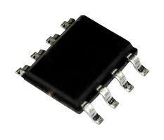
8 Terminations 3.3V 8 Pin INA219 Current regulator Zero-Drift Series -40°C~125°C Min 3V Max 5.5V
Unit Price: $1.058908
Ext Price: $1.06


8 Terminations 3.3V 8 Pin INA219 Current regulator Zero-Drift Series -40°C~125°C Min 3V Max 5.5V
The INA219 is an I2C-based high-side current and power monitor sensing 0-26V. Features 16 programmable addresses, 12-bit resolution, and an integrated math engine for direct power readout.
Product Introduction
Engineer's Takeaway
Positioning: The INA219 serves as a digital "power multimeter" for embedded systems, offloading the calculation of current and power from the host MCU by integrating a multiplier and calibration register.
Key Spec Highlight: The device senses bus voltages from 0V to 26V, typically independent of the supply voltage (3V to 5.5V), making it ideal for monitoring battery subsystems.
Supply Chain Status: High market availability. Due to "Maker Friendly" status (Adafruit/Arduino adoption), clone risk is present; verify trusted distributors for industrial designs.
1. Technical Architecture and Core Advantages
The INA219 is a zero-drift, bi-directional current/power monitor. Unlike simple analog current sense amplifiers, it integrates a 12-bit ADC and digital logic to report values directly over I2C.
1.1 Processing & Control
The core architecture is not a general-purpose MCU, but a specialized AFE with a Math Engine.
ADC: 12-bit Delta-Sigma converter.
Math Engine: Contains a programmable Calibration Register. It multiplies the Current Register value by the Bus Voltage Register value to calculate Power in watts.
Benefit: This architecture eliminates the need for the host processor to constantly poll voltage and current to perform multiplication, saving CPU cycles.
1.2 Peripherals & Interfaces
Communication: I2C interface supports Standard (100kHz) and Fast (400kHz) modes.
Addressing Logic: The logic distinguishes itself with 16 programmable addresses using only two pins (A0, A1).
Pins can be tied to GND, VS (Supply), SDA, or SCL to generate the matrix of addresses.
Alerts: Unlike the INA226, the INA219 lacks a dedicated ALERT pin, relying on register polling for data retrieval.

INA219 functional block diagram internal architecture
2. Naming / Variant Map and Selection Guide
2.1 Part Number Decoding
Texas Instruments uses specific suffixes to denote package and accuracy grades:
INA219: Base Series Name.
x (Grade):
A: Standard Grade (1% Max Shunt Voltage Error).
B: High-Accuracy Grade (0.5% Max Shunt Voltage Error).
yy (Package):
IDR: SOIC-8 (Standard surface mount).
CN: SOT-23-8 (Compact footprint).
2.2 Core Variant Comparison
| Variant | Accuracy (Max Error) | Package | Offset Voltage (Max) | Target Use |
|---|---|---|---|---|
| INA219A | 1.0% | SOIC-8 / SOT-23 | ±100 µV | General battery monitoring, consumer, maker projects |
| INA219B | 0.5% | SOIC-8 | ±50 µV | Precision instrumentation, server power rails |
3. Key Specifications Explained
Engineer's Note: The INA219 requires a separate supply voltage (Vs) of 3.0V to 5.5V. Do not confuse this with the Bus Voltage (Vbus) which can range 0V–26V.
3.1 Power & Operating Conditions
Bus Voltage Range (0V to 26V): The common-mode range allows the INA219 to monitor rails significantly higher than its own logic supply.
Input Bias Current: Typically 10µA. While low, this must be accounted for in ultra-low-power sleep designs if the monitor remains active.
Shunt Voltage: Supports ±40mV, ±80mV, ±160mV, or ±320mV ranges (programmable). Lower ranges reduce heat dissipation in the shunt resistor but reduce dynamic range.
3.2 Performance & Efficiency
Resolution: 12-bit ADC provides high granularity.
Conversion Time: Programmable from 84µs to 532μs (typically set to 532μs/12-bit for stability).
Filtering: Includes averaging options (up to 128 samples) to smooth out noisy power rails before the data is read by the MCU.
4. Design Notes and Common Integration Issues
4.1 PCB Layout Guidelines
To achieve the rated 0.5% accuracy, physical layout is as critical as register settings.
- Kelvin Connections: The IN+ and IN- traces must connect directly to the inner pads of the shunt resistor. Do not tap off the main high-current pours.
- Differential Pairs: Route IN+ and IN- as a differential pair to cancel noise coupling.
- Input Filters: Place 0.1µF ceramic capacitors close to the VS pin. If sensing noisy motor loads, an RC filter (10Ω + 0.1µF) on the input lines can prevent aliasing, though it introduces a slight gain error.

INA219 Pinout and package footprint
4.2 Debugging Common Faults (Pain Points)
Problem 1: Accuracy Errors (Reading does not match Multimeter)
Symptom: Current readings are off by >5-10%.
Fix: This is usually a Calibration Register issue. The INA219 does not output raw current; it outputs a value based on the Calibration_Register which you must calculate based on your exact Shunt Resistor (R_shunt) and desired Least Significant Bit (LSB).
* Ref: Firmware/Calibration mismatch.
Problem 2: I2C Addressing Conflicts
Symptom: Device NACKs or multiple sensors conflict.
Fix: Check soldered connections on A0 and A1. A cold solder joint to GND (default address 0x40) or an accidental bridge can shift the address. Verify against the 16-address table in the datasheet.
Problem 3: Thermal Failure / Magic Smoke
Symptom: Chip failure on power-up or load dump.
Fix: The Absolute Max rating is 30V. Inductive spikes (movies, relays) on a 24V line can easily exceed 30V. Clamp the bus using a TVS diode (e.g., SMBJ26A) to protect the IN+ pin.
5. Typical Applications
📺 Video Recommendation: INA219 Guide
5.1 System Integration Analysis
Application: Digital Power Supply FeedbackIn variable bench power supplies, the INA219 replaces discrete current sense amps. - Why INA219? It measures voltage at the load (Bus Voltage) and Current simultaneously. - Integration: The MCU reads the Power Register via I2C to update the LCD display and adjusts the PWM duty cycle if the Current Register exceeds the safety limit (Software Over-Current Protection).

INA219 Typical application circuit with Shunt Resistor (Rs)
6. Competitors and Alternatives
| Competitor | Comparison to INA219 |
|---|---|
| INA226 (TI) | Higher Precision. Offers 16-bit resolution and alerts. 36V Bus. Migration path if 12-bit INA219 is insufficient. |
| INA233 (TI) | PMBus Support. Similar performance but uses PMBus protocol, standard in server/telecom management. |
| ACS712 | Isolation. Uses Hall Effect. Lower accuracy/higher drift, but provides galvanic isolation for high-voltage mains. |
| MAX9611 (Maxim) | Integrated FET Driver. Combines current sensing with fan control/actuation. |
7. FAQ
Q: What is the absolute maximum voltage for INA219?
A: The distinct bus voltage limit is 30V (Absolute Max), with recommended operation up to 26V. Exceeding this destroys the input pins.
Q: Can the INA219 measure current on the low side (Ground return)?
A: While technically possible if the common-mode constraints overlap, the INA219 is designed and optimized for High-Side sensing. Low-side sensing disturbs the system ground reference.
Q: How do I select the Shunt Resistor value?
A: Balance power loss with signal size.
V_shunt_max / Max_Current = R_shunt. For 3.2A max current with ±320mV range, a 0.1Ω resistor is ideal.Q: Why does the INA219 return zero current?
A: Confirm the
Configuration Registeris set to "Continuous" mode and theCalibration Registeris non-zero. The default startup state requires initialization.
8. Resources and Downloads
Datasheet: INA219 Product Data
Dev Tools: Adafruit INA219 Breakout (PID 904), SparkFun Current Sensor Breakout
Specifications
- TypeParameter
- Factory Lead Time12 Weeks
- Mounting Type
The "Mounting Type" in electronic components refers to the method used to attach or connect a component to a circuit board or other substrate, such as through-hole, surface-mount, or panel mount.
Surface Mount - Package / Case
refers to the protective housing that encases an electronic component, providing mechanical support, electrical connections, and thermal management.
SOT-23-8 - Surface Mount
having leads that are designed to be soldered on the side of a circuit board that the body of the component is mounted on.
YES - Number of Pins8
- Operating Temperature
The operating temperature is the range of ambient temperature within which a power supply, or any other electrical equipment, operate in. This ranges from a minimum operating temperature, to a peak or maximum operating temperature, outside which, the power supply may fail.
-40°C~125°C - Packaging
Semiconductor package is a carrier / shell used to contain and cover one or more semiconductor components or integrated circuits. The material of the shell can be metal, plastic, glass or ceramic.
Tape & Reel (TR) - Series
In electronic components, the "Series" refers to a group of products that share similar characteristics, designs, or functionalities, often produced by the same manufacturer. These components within a series typically have common specifications but may vary in terms of voltage, power, or packaging to meet different application needs. The series name helps identify and differentiate between various product lines within a manufacturer's catalog.
Zero-Drift - JESD-609 Code
The "JESD-609 Code" in electronic components refers to a standardized marking code that indicates the lead-free solder composition and finish of electronic components for compliance with environmental regulations.
e4 - Part Status
Parts can have many statuses as they progress through the configuration, analysis, review, and approval stages.
Active - Moisture Sensitivity Level (MSL)
Moisture Sensitivity Level (MSL) is a standardized rating that indicates the susceptibility of electronic components, particularly semiconductors, to moisture-induced damage during storage and the soldering process, defining the allowable exposure time to ambient conditions before they require special handling or baking to prevent failures
2 (1 Year) - Number of Terminations8
- ECCN Code
An ECCN (Export Control Classification Number) is an alphanumeric code used by the U.S. Bureau of Industry and Security to identify and categorize electronic components and other dual-use items that may require an export license based on their technical characteristics and potential for military use.
EAR99 - Terminal Finish
Terminal Finish refers to the surface treatment applied to the terminals or leads of electronic components to enhance their performance and longevity. It can improve solderability, corrosion resistance, and overall reliability of the connection in electronic assemblies. Common finishes include nickel, gold, and tin, each possessing distinct properties suitable for various applications. The choice of terminal finish can significantly impact the durability and effectiveness of electronic devices.
Nickel/Palladium/Gold (Ni/Pd/Au) - Terminal Position
In electronic components, the term "Terminal Position" refers to the physical location of the connection points on the component where external electrical connections can be made. These connection points, known as terminals, are typically used to attach wires, leads, or other components to the main body of the electronic component. The terminal position is important for ensuring proper connectivity and functionality of the component within a circuit. It is often specified in technical datasheets or component specifications to help designers and engineers understand how to properly integrate the component into their circuit designs.
DUAL - Terminal Form
Occurring at or forming the end of a series, succession, or the like; closing; concluding.
GULL WING - Peak Reflow Temperature (Cel)
Peak Reflow Temperature (Cel) is a parameter that specifies the maximum temperature at which an electronic component can be exposed during the reflow soldering process. Reflow soldering is a common method used to attach electronic components to a circuit board. The Peak Reflow Temperature is crucial because it ensures that the component is not damaged or degraded during the soldering process. Exceeding the specified Peak Reflow Temperature can lead to issues such as component failure, reduced performance, or even permanent damage to the component. It is important for manufacturers and assemblers to adhere to the recommended Peak Reflow Temperature to ensure the reliability and functionality of the electronic components.
260 - Supply Voltage
Supply voltage refers to the electrical potential difference provided to an electronic component or circuit. It is crucial for the proper operation of devices, as it powers their functions and determines performance characteristics. The supply voltage must be within specified limits to ensure reliability and prevent damage to components. Different electronic devices have specific supply voltage requirements, which can vary widely depending on their design and intended application.
3.3V - Terminal Pitch
The center distance from one pole to the next.
0.65mm - Base Part Number
The "Base Part Number" (BPN) in electronic components serves a similar purpose to the "Base Product Number." It refers to the primary identifier for a component that captures the essential characteristics shared by a group of similar components. The BPN provides a fundamental way to reference a family or series of components without specifying all the variations and specific details.
INA219 - Function
The parameter "Function" in electronic components refers to the specific role or purpose that the component serves within an electronic circuit. It defines how the component interacts with other elements, influences the flow of electrical signals, and contributes to the overall behavior of the system. Functions can include amplification, signal processing, switching, filtering, and energy storage, among others. Understanding the function of each component is essential for designing effective and efficient electronic systems.
Current Monitor - Number of Channels2
- Max Supply Voltage
In general, the absolute maximum common-mode voltage is VEE-0.3V and VCC+0.3V, but for products without a protection element at the VCC side, voltages up to the absolute maximum rated supply voltage (i.e. VEE+36V) can be supplied, regardless of supply voltage.
5.5V - Min Supply Voltage
The minimum supply voltage (V min ) is explored for sequential logic circuits by statistically simulating the impact of within-die process variations and gate-dielectric soft breakdown on data retention and hold time.
3V - Analog IC - Other Type
Analog IC - Other Type is a parameter used to categorize electronic components that are integrated circuits (ICs) designed for analog signal processing but do not fall into more specific subcategories such as amplifiers, comparators, or voltage regulators. These ICs may include specialized analog functions such as analog-to-digital converters (ADCs), digital-to-analog converters (DACs), voltage references, or signal conditioning circuits. They are typically used in various applications where precise analog signal processing is required, such as in audio equipment, instrumentation, communication systems, and industrial control systems. Manufacturers provide detailed specifications for these components to help engineers select the most suitable IC for their specific design requirements.
POWER SUPPLY SUPPORT CIRCUIT - Nominal Supply Current
Nominal current is the same as the rated current. It is the current drawn by the motor while delivering rated mechanical output at its shaft.
1mA - Adjustable Threshold
The "Adjustable Threshold" parameter in electronic components refers to the ability to manually set or modify the threshold level at which a specific function or operation is triggered. This feature allows users to customize the sensitivity or activation point of the component according to their specific requirements or preferences. By adjusting the threshold, users can fine-tune the performance of the component to suit different applications or environmental conditions. This flexibility in threshold adjustment can be particularly useful in various electronic devices and systems where precise control over triggering levels is necessary for optimal functionality.
NO - Quiescent Current
The quiescent current is defined as the current level in the amplifier when it is producing an output of zero.
700μA - Accuracy
Accuracy in electronic components refers to the degree to which a measured value agrees with the true or accepted value. It evaluates the precision of a component in providing correct output or measurement under specified conditions. High accuracy indicates minimal deviation from the actual value, while low accuracy shows significant error in measurement. This parameter is crucial in applications where precise data is essential for reliable performance and decision-making.
±1% - Common Mode Rejection Ratio
Common Mode Rejection Ratio (CMRR) is a measure of the ability of a differential amplifier to reject input signals that are common to both input terminals. It is defined as the ratio of the differential gain to the common mode gain. A high CMRR indicates that the amplifier can effectively eliminate noise and interference that affects both inputs simultaneously, enhancing the fidelity of the amplified signal. CMRR is typically expressed in decibels (dB), with higher values representing better performance in rejecting common mode signals.
100 dB - Threshold Voltage
The threshold voltage is a critical parameter in electronic components, particularly in field-effect transistors (FETs). It refers to the minimum voltage required at the input terminal of the FET to turn it on and allow current to flow between the source and drain terminals. Below the threshold voltage, the FET remains in the off state, acting as an open switch. Once the threshold voltage is exceeded, the FET enters the on state, conducting current between the source and drain.The threshold voltage is a key factor in determining the operating characteristics of FETs, such as their switching speed and power consumption. It is typically specified by the manufacturer and can vary depending on the specific type of FET and its design. Designers must consider the threshold voltage when selecting FETs for a particular application to ensure proper functionality and performance.
+2 - Sensing Method
The sensing method in electronic components refers to the technique or mechanism used to detect and measure physical phenomena such as temperature, pressure, light, or motion. This includes a variety of technologies such as resistive, capacitive, inductive, and optical sensing methods. The choice of sensing method affects the accuracy, response time, and application suitability of the electronic component. It plays a crucial role in determining how effectively a device can interact with and interpret its environment.
High-Side - Length2.9mm
- Height Seated (Max)
Height Seated (Max) is a parameter in electronic components that refers to the maximum allowable height of the component when it is properly seated or installed on a circuit board or within an enclosure. This specification is crucial for ensuring proper fit and alignment within the overall system design. Exceeding the maximum seated height can lead to mechanical interference, electrical shorts, or other issues that may impact the performance and reliability of the electronic device. Manufacturers provide this information to help designers and engineers select components that will fit within the designated space and function correctly in the intended application.
1.45mm - Width1.6mm
- Radiation Hardening
Radiation hardening is the process of making electronic components and circuits resistant to damage or malfunction caused by high levels of ionizing radiation, especially for environments in outer space (especially beyond the low Earth orbit), around nuclear reactors and particle accelerators, or during nuclear accidents or nuclear warfare.
No - RoHS Status
RoHS means “Restriction of Certain Hazardous Substances” in the “Hazardous Substances Directive” in electrical and electronic equipment.
ROHS3 Compliant - Lead Free
Lead Free is a term used to describe electronic components that do not contain lead as part of their composition. Lead is a toxic material that can have harmful effects on human health and the environment, so the electronics industry has been moving towards lead-free components to reduce these risks. Lead-free components are typically made using alternative materials such as silver, copper, and tin. Manufacturers must comply with regulations such as the Restriction of Hazardous Substances (RoHS) directive to ensure that their products are lead-free and environmentally friendly.
Lead Free
Parts with Similar Specs
Datasheet PDF
- PCN Design/Specification :
![LR44 VS A76[Video+FAQ]: Are they interchangeable?](https://res.utmel.com/Images/Article/f19969bd-7854-4054-9cff-b90a5521ab6d.png) LR44 VS A76[Video+FAQ]: Are they interchangeable?
LR44 VS A76[Video+FAQ]: Are they interchangeable?26 April 202224469
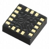 LIS3DH Accelerometer: Datasheet, Pinout, Functionality, and Block Diagram
08 July 20216082
 LM334D Adjustable Current Source: Feature, Specification, and Datasheet
03 July 2021789
 VL53L1X Laser-Ranging Sensor: Datasheet, Pinout and Schematic
29 July 202111251
 STM32F103CBT6 - STM - Microcontroller
29 April 20216710
![Is LM317 better than LM7805?[video+FAQ]](https://res.utmel.com/Images/Article/5cafb24b-3f28-4935-b123-c59a0f9c15eb.jpg) Is LM317 better than LM7805?[video+FAQ]
Is LM317 better than LM7805?[video+FAQ]27 April 20228692
 LM7809 Voltage Regulator IC: Equivalent, Pinout and Datasheet
14 September 202114336
 ATTINY20 8-bit AVR Microcontroller: Pinout, Features and Datasheet
22 March 20221289
 What are Quantum Sensors?
27 October 20212405
 Selection and Optimization of Peripheral Components for DC-DC Boost Regulator
15 April 20221976
 Use the Renesas AE-CLOUD2 to Send GPS Data to the Google Cloud IoT
15 November 20191279
 UTMEL- Sale Promotion
20 June 20234125
 Optimizing Energy Exchange with Vehicle-to-Grid Technology
25 April 20232873
 How do We Select Automotive Relays?
30 September 20209926
 GaN-Based Transistors for High-Frequency DC-DC Converter Applications
06 July 20234720
 Introduction to BGA Package
07 December 20215020
Texas Instruments
In Stock: 130
Minimum: 1 Multiples: 1
Qty
Unit Price
Ext Price
1
$1.058908
$1.06
10
$0.998970
$9.99
100
$0.942424
$94.24
500
$0.889080
$444.54
1000
$0.838754
$838.75
Not the price you want? Send RFQ Now and we'll contact you ASAP.
Inquire for More Quantity
![INA226AIDGSR]() INA226AIDGSR
INA226AIDGSRTexas Instruments
![LM334Z/NOPB]() LM334Z/NOPB
LM334Z/NOPBTexas Instruments
![LM334MX/NOPB]() LM334MX/NOPB
LM334MX/NOPBTexas Instruments
![LM334M/NOPB]() LM334M/NOPB
LM334M/NOPBTexas Instruments
![INA219BIDCNT]() INA219BIDCNT
INA219BIDCNTTexas Instruments
![INA220AIDGST]() INA220AIDGST
INA220AIDGSTTexas Instruments
![INA138NA/250]() INA138NA/250
INA138NA/250Texas Instruments
![INA168NA/3K]() INA168NA/3K
INA168NA/3KTexas Instruments
![INA193AIDBVR]() INA193AIDBVR
INA193AIDBVRTexas Instruments
![INA169NA/250]() INA169NA/250
INA169NA/250Texas Instruments


