
IR2112 Driver IC: Circuit, Pinout and Datasheet

Through Hole Tube Obsolete EAR99 Gate Drivers ICs Non-Inverting 2 600V V 14-DIP (0.300, 7.62mm) IR2112


Through Hole Tube Obsolete EAR99 Gate Drivers ICs Non-Inverting 2 600V V 14-DIP (0.300, 7.62mm) IR2112
Hello everyone, welcome to the new post today. The IR2112 is a high voltage IC that acts as a MOSFET driver and IGBT driver. This article mainly introduces circuit, pinout, datasheet, and other detailed information about Infineon Technologies IR2112.
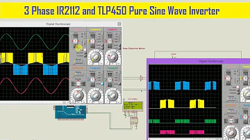
3 Phase IR2112 & TLP450 Pure Sine Wave Inverter Comparison | VFD | Code | Schematics | PCB Design
IR2112 Description
The IR2112 is a high voltage IC that acts as a MOSFET driver and IGBT driver. It has independent high and low-side referenced output channels with a threshold voltage of 600 V.
Bootstrap feature makes it compatible with high-side driver applications. Additionally, it has Schmitt triggered inputs that are compatible with the standard CMOS and LSTTL outputs. The voltage range is 10V to 20V.
Furthermore, it has applications that require the circuitry of both high and low-side drive, for example, half-bridge and full-bridge circuits. It is available in 14 Lead PDIP and 16 lead SOIC packages.
IR2112 Pinout

IR2112 Pinout
| Pin Number | Pin Name | Description |
| 1 | LO | Logic supply |
| 2 | COM | Logic input for high side gate driver output (HO), in phase |
| 3 | VCC | Logic input for shutdown |
| 5 | VS | Logic input for low side gate driver output (LO), in phase |
| 6 | VB | Logic ground |
| 7 | HO | High side floating supply |
| 9 | VDD | High side gate drive output |
| 10 | HIN | High side floating supply return |
| 11 | SD | Low side supply |
| 12 | LIN | Low side gate drive output |
| 13 | VSS | Low side return |
IR2112 Pin Description
IR2112 CAD Model

Symbol

Footprint

3D Model
IR2112 Features
-High and low side driver IC with source current 0.25 A and sink current 0.5 A
-It can tolerate negative transient voltage
-The range of separate voltage supply is from 3.3V to 20V and gate driver supply range is from 10 to 20 V
-floating channel designed for bootstrap operation
-Inputs and outputs are in phase
-Matched propagation delay and under-voltage lockout for both channels
-Threshold voltage is +600 V
-Cycle by cycle edge-triggered shutdown logic
-3.3V logic compatible
-Logic and power ground ±5V offset
-CMOS Schmitt-triggered inputs with pull-down
Specifications
- TypeParameter
- Mounting Type
The "Mounting Type" in electronic components refers to the method used to attach or connect a component to a circuit board or other substrate, such as through-hole, surface-mount, or panel mount.
Through Hole - Package / Case
refers to the protective housing that encases an electronic component, providing mechanical support, electrical connections, and thermal management.
14-DIP (0.300, 7.62mm) - Surface Mount
having leads that are designed to be soldered on the side of a circuit board that the body of the component is mounted on.
NO - Driver ConfigurationHigh-Side or Low-Side
- Logic voltage-VIL, VIH6V 9.5V
- Operating Temperature
The operating temperature is the range of ambient temperature within which a power supply, or any other electrical equipment, operate in. This ranges from a minimum operating temperature, to a peak or maximum operating temperature, outside which, the power supply may fail.
-40°C~150°C TJ - Packaging
Semiconductor package is a carrier / shell used to contain and cover one or more semiconductor components or integrated circuits. The material of the shell can be metal, plastic, glass or ceramic.
Tube - Published1996
- Part Status
Parts can have many statuses as they progress through the configuration, analysis, review, and approval stages.
Obsolete - Moisture Sensitivity Level (MSL)
Moisture Sensitivity Level (MSL) is a standardized rating that indicates the susceptibility of electronic components, particularly semiconductors, to moisture-induced damage during storage and the soldering process, defining the allowable exposure time to ambient conditions before they require special handling or baking to prevent failures
1 (Unlimited) - Number of Terminations14
- ECCN Code
An ECCN (Export Control Classification Number) is an alphanumeric code used by the U.S. Bureau of Industry and Security to identify and categorize electronic components and other dual-use items that may require an export license based on their technical characteristics and potential for military use.
EAR99 - Voltage - Supply
Voltage - Supply refers to the range of voltage levels that an electronic component or circuit is designed to operate with. It indicates the minimum and maximum supply voltage that can be applied for the device to function properly. Providing supply voltages outside this range can lead to malfunction, damage, or reduced performance. This parameter is critical for ensuring compatibility between different components in a circuit.
10V~20V - Terminal Position
In electronic components, the term "Terminal Position" refers to the physical location of the connection points on the component where external electrical connections can be made. These connection points, known as terminals, are typically used to attach wires, leads, or other components to the main body of the electronic component. The terminal position is important for ensuring proper connectivity and functionality of the component within a circuit. It is often specified in technical datasheets or component specifications to help designers and engineers understand how to properly integrate the component into their circuit designs.
DUAL - Peak Reflow Temperature (Cel)
Peak Reflow Temperature (Cel) is a parameter that specifies the maximum temperature at which an electronic component can be exposed during the reflow soldering process. Reflow soldering is a common method used to attach electronic components to a circuit board. The Peak Reflow Temperature is crucial because it ensures that the component is not damaged or degraded during the soldering process. Exceeding the specified Peak Reflow Temperature can lead to issues such as component failure, reduced performance, or even permanent damage to the component. It is important for manufacturers and assemblers to adhere to the recommended Peak Reflow Temperature to ensure the reliability and functionality of the electronic components.
NOT SPECIFIED - Number of Functions1
- Supply Voltage
Supply voltage refers to the electrical potential difference provided to an electronic component or circuit. It is crucial for the proper operation of devices, as it powers their functions and determines performance characteristics. The supply voltage must be within specified limits to ensure reliability and prevent damage to components. Different electronic devices have specific supply voltage requirements, which can vary widely depending on their design and intended application.
15V - Time@Peak Reflow Temperature-Max (s)
Time@Peak Reflow Temperature-Max (s) refers to the maximum duration that an electronic component can be exposed to the peak reflow temperature during the soldering process, which is crucial for ensuring reliable solder joint formation without damaging the component.
NOT SPECIFIED - Base Part Number
The "Base Part Number" (BPN) in electronic components serves a similar purpose to the "Base Product Number." It refers to the primary identifier for a component that captures the essential characteristics shared by a group of similar components. The BPN provides a fundamental way to reference a family or series of components without specifying all the variations and specific details.
IR2112 - JESD-30 Code
JESD-30 Code refers to a standardized descriptive designation system established by JEDEC for semiconductor-device packages. This system provides a systematic method for generating designators that convey essential information about the package's physical characteristics, such as size and shape, which aids in component identification and selection. By using JESD-30 codes, manufacturers and engineers can ensure consistency and clarity in the specification of semiconductor packages across various applications and industries.
R-PDIP-T14 - Qualification Status
An indicator of formal certification of qualifications.
Not Qualified - Input Type
Input type in electronic components refers to the classification of the signal or data that a component can accept for processing or conversion. It indicates whether the input is analog, digital, or a specific format such as TTL or CMOS. Understanding input type is crucial for ensuring compatibility between different electronic devices and circuits, as it determines how signals are interpreted and interacted with.
Non-Inverting - Rise / Fall Time (Typ)
The parameter "Rise / Fall Time (Typ)" in electronic components refers to the time it takes for a signal to transition from a specified low level to a specified high level (rise time) or from a high level to a low level (fall time). It is typically measured in nanoseconds or picoseconds and is an important characteristic in determining the speed and performance of a component, such as a transistor or integrated circuit. A shorter rise/fall time indicates faster signal switching and can impact the overall speed and efficiency of a circuit. Designers often consider this parameter when selecting components for high-speed applications to ensure proper signal integrity and timing.
80ns 40ns - Interface IC Type
The parameter "Interface IC Type" in electronic components refers to the type of integrated circuit (IC) that is used to facilitate communication between different electronic devices or subsystems. This IC is responsible for managing the exchange of data and control signals between the devices, ensuring proper communication and coordination. The specific type of interface IC used can vary depending on the requirements of the system, such as serial communication (e.g., UART, SPI, I2C), parallel communication, or specialized interfaces like USB or Ethernet. Choosing the appropriate interface IC type is crucial for ensuring compatibility, reliability, and efficiency in electronic systems.
HALF BRIDGE BASED MOSFET DRIVER - Channel Type
In electronic components, the parameter "Channel Type" refers to the type of channel through which electrical signals or current flow within the component. This parameter is commonly associated with field-effect transistors (FETs) and other semiconductor devices. The channel type can be categorized as either N-channel or P-channel, depending on the polarity of the majority charge carriers (electrons or holes) that carry the current within the channel. N-channel devices have an electron-conducting channel, while P-channel devices have a hole-conducting channel. Understanding the channel type is crucial for proper circuit design and component selection to ensure compatibility and optimal performance.
Independent - Number of Drivers2
- Turn On Time
The time that it takes a gate circuit to allow a current to reach its full value.
0.18 μs - Output Peak Current Limit-Nom
Output Peak Current Limit-Nom is a parameter in electronic components that specifies the maximum current that can be delivered by the output under normal operating conditions. This limit is typically set to protect the component from damage due to excessive current flow. It ensures that the component operates within its safe operating limits and prevents overheating or other potential issues. Designers and engineers use this parameter to ensure proper functioning and reliability of the electronic system in which the component is used.
0.5A - Gate Type
In electronic components, the term "Gate Type" typically refers to the type of logic gate used in digital circuits. A logic gate is a fundamental building block of digital circuits that performs a specific logical operation based on the input signals it receives. Common types of logic gates include AND, OR, NOT, NAND, NOR, XOR, and XNOR gates.The Gate Type parameter specifies the specific logic function that the gate performs, such as AND, OR, or NOT. Different gate types have different truth tables that define their behavior based on the input signals. By selecting the appropriate gate type for a given application, designers can implement various logical functions and operations in digital circuits.Understanding the gate type is essential for designing and analyzing digital circuits, as it determines how the circuit processes and manipulates binary data. Choosing the right gate type is crucial for ensuring the correct functionality and performance of the digital system being designed.
IGBT, N-Channel MOSFET - Current - Peak Output (Source, Sink)
The parameter "Current - Peak Output (Source, Sink)" in electronic components refers to the maximum amount of current that the component can either supply (source) or sink (absorb) under peak conditions. This parameter is important for understanding the capability of the component to handle sudden surges or spikes in current without being damaged. The peak output current is typically specified in datasheets and is crucial for designing circuits that require high current handling capabilities. It is essential to consider this parameter to ensure the component operates within its safe operating limits and to prevent potential damage or malfunction.
250mA 500mA - High Side Driver
A High Side Driver is an electronic component used in power management applications to control the switching of high-side power devices such as MOSFETs or IGBTs. It is designed to drive the gate or base of the power device to turn it on or off, allowing current to flow through the load or cutting off the current flow. High Side Drivers are commonly used in automotive, industrial, and consumer electronics to control various loads such as motors, solenoids, and heaters. They provide isolation between the control circuitry and the high-side power device, ensuring safe and reliable operation of the system.
YES - Turn Off Time
Turn Off Time is a parameter in electronic components, particularly in devices like transistors and diodes. It refers to the time taken for the component to switch from an ON state to an OFF state when a control signal is applied. This parameter is crucial in determining the speed and efficiency of the component's operation. A shorter turn off time indicates faster switching speeds, which is important in applications where rapid switching is required, such as in power electronics and digital circuits. Manufacturers provide this specification in datasheets to help engineers and designers select the right components for their specific requirements.
0.16 μs - High Side Voltage - Max (Bootstrap)
The parameter "High Side Voltage - Max (Bootstrap)" in electronic components refers to the maximum voltage that can be applied to the high side of a bootstrap circuit. Bootstrap circuits are commonly used in power electronics to drive high-side MOSFETs or IGBTs efficiently. This parameter is crucial for ensuring the proper operation and reliability of the bootstrap circuit, as exceeding the maximum voltage can lead to component failure or malfunction. Designers must carefully consider this specification when selecting components and designing circuits to prevent damage and ensure optimal performance.
600V - Length19.305mm
- Height Seated (Max)
Height Seated (Max) is a parameter in electronic components that refers to the maximum allowable height of the component when it is properly seated or installed on a circuit board or within an enclosure. This specification is crucial for ensuring proper fit and alignment within the overall system design. Exceeding the maximum seated height can lead to mechanical interference, electrical shorts, or other issues that may impact the performance and reliability of the electronic device. Manufacturers provide this information to help designers and engineers select components that will fit within the designated space and function correctly in the intended application.
5.33mm - RoHS Status
RoHS means “Restriction of Certain Hazardous Substances” in the “Hazardous Substances Directive” in electrical and electronic equipment.
Non-RoHS Compliant
IR2112 Equivalent
IR2110, IR2118, IR2101, IR2102, IR2104, IR2106, IR2184
IR2112 Alternatives
| Part Number | Description | Manufacturer |
| IR2112DRIVERS AND INTERFACES | Half Bridge Based MOSFET Driver, 0.5A, CMOS, PDIP14, PLASTIC, MS-001AC, DIP-14 | International Rectifier |
| IR2112PBFDRIVERS AND INTERFACES | Half Bridge Based MOSFET Driver, 0.5A, CMOS, PDIP14, LEAD-FREE, PLASTIC, MS-001AC, DIP-14 | Infineon Technologies AG |
IR2112 Functional Block Diagram

IR2112 Functional Block Diagram
Where to use IR2112 ?
This IC can be used as both a Mosfet driver and an IGBT driver. These IC’s are commonly used in half-bridge circuits for switching Mosfets. You can use this IC in high-frequency applications due to its matched propagation delays. It is used in high voltage applications for switching discrete power Mosfets ON and OFF using low voltage input.
How to use IR2112?
The connection diagram of this IC IR2112 is shown in the figure below. HIN and LIN are the input signals for the high and low driver sides. They connect to some microcontroller or a voltage supply through a switch and are provided with an input signal of range 4 to 5V. It has a shutdown pin which is provided to protect the circuit in case of overvoltages or current by connecting this pin to +5V. It will shut down the circuit.

Typical Connection
IR2112 Circuit

Floating Supply Voltage Transient Test Circuit

Switching Time Test Circuit
IR2112 Applications
▲Used in designing H-bridge, half-bridge, and full-bridge circuits
▲Used in switched-mode power supplies
▲Used in inverters, traction motor control, and induction heating.
IR2112 Case Outline

IR2112 Case Outline
IR2112 Manufacturer
Infineon Technologies AG is a German semiconductor manufacturer founded in 1999 when the semiconductor operations of the former parent company Siemens AG were spun off. Infineon has about 46,665 employees and is one of the ten largest semiconductor manufacturers worldwide. It is the market leader in automotive and power semiconductors.
Trend Analysis
Datasheet PDF
- Datasheets :
- Other Related Documents :
 INA115BU Instrumentation Amplifier:Datasheet, Application, Circuit
17 September 20211286
 A Comparison Article about L293D & ULN2003
25 April 20225962
 CR2016 Battery: Pinout, Equivalents, CR2016 vs. CR2032
06 October 20212297
![CP2104 USB-to-UART Bridge: Features, Pinout, CP2102 vs. CP2104 [Video&FAQ]](https://res.utmel.com/Images/Article/1b31b768-9825-4c49-a68b-dc56d2fd6121.png) CP2104 USB-to-UART Bridge: Features, Pinout, CP2102 vs. CP2104 [Video&FAQ]
CP2104 USB-to-UART Bridge: Features, Pinout, CP2102 vs. CP2104 [Video&FAQ]06 May 20225454
 FGA25N120 IGBT: Application, Datasheet, Pinout
14 October 202111863
 STM32F407VGT6 Microcontroller: 168MHz,100-LQFP, Pinout and Features
07 February 20229878
 MPSA14 Darlington Transistor: Datasheet, Equivalent, Pinout
08 December 20213241
 NXP MINISASTOCSI Camera Module Guide and Community Solutions
09 June 202589
 Detailed Analysis of Analog IC
22 November 20212722
 Top 10 High-Performance End Mills for Metalworking in 2025
17 July 2025547
 What is RFID?
23 March 20214278
 Introduction to Synchronous Counter and Asynchronous Counter
31 March 202513425
 Power Transformer Basics and Operation Cautions
16 October 20203357
 Apple M1 Ultra -- The Technology Behind the Chip Interconnection
12 March 20223657
 How to make an Obstacle Avoiding Robot?
29 August 20237936
 Modeling, Modulation Analysis of Filter-Integrated Three-Switch Boost Inverter
12 April 20232496
Infineon Technologies
In Stock: 10000
United States
China
Canada
Japan
Russia
Germany
United Kingdom
Singapore
Italy
Hong Kong(China)
Taiwan(China)
France
Korea
Mexico
Netherlands
Malaysia
Austria
Spain
Switzerland
Poland
Thailand
Vietnam
India
United Arab Emirates
Afghanistan
Åland Islands
Albania
Algeria
American Samoa
Andorra
Angola
Anguilla
Antigua & Barbuda
Argentina
Armenia
Aruba
Australia
Azerbaijan
Bahamas
Bahrain
Bangladesh
Barbados
Belarus
Belgium
Belize
Benin
Bermuda
Bhutan
Bolivia
Bonaire, Sint Eustatius and Saba
Bosnia & Herzegovina
Botswana
Brazil
British Indian Ocean Territory
British Virgin Islands
Brunei
Bulgaria
Burkina Faso
Burundi
Cabo Verde
Cambodia
Cameroon
Cayman Islands
Central African Republic
Chad
Chile
Christmas Island
Cocos (Keeling) Islands
Colombia
Comoros
Congo
Congo (DRC)
Cook Islands
Costa Rica
Côte d’Ivoire
Croatia
Cuba
Curaçao
Cyprus
Czechia
Denmark
Djibouti
Dominica
Dominican Republic
Ecuador
Egypt
El Salvador
Equatorial Guinea
Eritrea
Estonia
Eswatini
Ethiopia
Falkland Islands
Faroe Islands
Fiji
Finland
French Guiana
French Polynesia
Gabon
Gambia
Georgia
Ghana
Gibraltar
Greece
Greenland
Grenada
Guadeloupe
Guam
Guatemala
Guernsey
Guinea
Guinea-Bissau
Guyana
Haiti
Honduras
Hungary
Iceland
Indonesia
Iran
Iraq
Ireland
Isle of Man
Israel
Jamaica
Jersey
Jordan
Kazakhstan
Kenya
Kiribati
Kosovo
Kuwait
Kyrgyzstan
Laos
Latvia
Lebanon
Lesotho
Liberia
Libya
Liechtenstein
Lithuania
Luxembourg
Macao(China)
Madagascar
Malawi
Maldives
Mali
Malta
Marshall Islands
Martinique
Mauritania
Mauritius
Mayotte
Micronesia
Moldova
Monaco
Mongolia
Montenegro
Montserrat
Morocco
Mozambique
Myanmar
Namibia
Nauru
Nepal
New Caledonia
New Zealand
Nicaragua
Niger
Nigeria
Niue
Norfolk Island
North Korea
North Macedonia
Northern Mariana Islands
Norway
Oman
Pakistan
Palau
Palestinian Authority
Panama
Papua New Guinea
Paraguay
Peru
Philippines
Pitcairn Islands
Portugal
Puerto Rico
Qatar
Réunion
Romania
Rwanda
Samoa
San Marino
São Tomé & Príncipe
Saudi Arabia
Senegal
Serbia
Seychelles
Sierra Leone
Sint Maarten
Slovakia
Slovenia
Solomon Islands
Somalia
South Africa
South Sudan
Sri Lanka
St Helena, Ascension, Tristan da Cunha
St. Barthélemy
St. Kitts & Nevis
St. Lucia
St. Martin
St. Pierre & Miquelon
St. Vincent & Grenadines
Sudan
Suriname
Svalbard & Jan Mayen
Sweden
Syria
Tajikistan
Tanzania
Timor-Leste
Togo
Tokelau
Tonga
Trinidad & Tobago
Tunisia
Turkey
Turkmenistan
Turks & Caicos Islands
Tuvalu
U.S. Outlying Islands
U.S. Virgin Islands
Uganda
Ukraine
Uruguay
Uzbekistan
Vanuatu
Vatican City
Venezuela
Wallis & Futuna
Yemen
Zambia
Zimbabwe
![IR2113PBF]() IR2113PBF
IR2113PBFInfineon Technologies
![IR2110SPBF]() IR2110SPBF
IR2110SPBFInfineon Technologies
![IR2104SPBF]() IR2104SPBF
IR2104SPBFInfineon Technologies
![IR2184SPBF]() IR2184SPBF
IR2184SPBFInfineon Technologies
![IR2181SPBF]() IR2181SPBF
IR2181SPBFInfineon Technologies
![IR2183SPBF]() IR2183SPBF
IR2183SPBFInfineon Technologies
![IRS2113STRPBF]() IRS2113STRPBF
IRS2113STRPBFInfineon Technologies
![IR2153SPBF]() IR2153SPBF
IR2153SPBFInfineon Technologies
![IR2214SSPBF]() IR2214SSPBF
IR2214SSPBFInfineon Technologies
![IR2102SPBF]() IR2102SPBF
IR2102SPBFInfineon Technologies


