
 Product
 Brand
Brand Articles
 Tools
Tools
IRF620 N-Channel Power MOSFET: Datasheet pdf, 6A 200V MOSFET and Pinout


N-Channel Tube 800m Ω @ 3A, 10V ±20V 350pF @ 25V 27nC @ 10V TO-220-3
IRF620 is a 6A 200V N-Channel Power MOSFET N-Channel enhancement mode power field effect transistors are produced using Fairchild’s proprietary, planar, DMOS technology. This article is going to introduce details about IRF620 MOSFET.

Building the MOSFET SSR using IRF620s
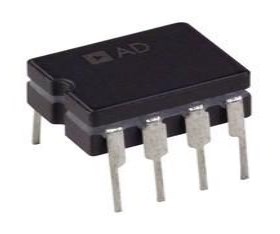
IRF620 Description
IRF620 is a 6A 200V N -Channel Power MOSFET N -Channel enhancement mode power field effect transistors are produced using Fairchild’s proprietary, planar, DMOS technology.
This device has been carefully designed to decrease on-state resistance, provide improved switching performance, and withstand high-energy pulses. These devices are ideal for high-efficiency switching DC/DC converters, switch-mode power supplies, and DC-AC converters for continuous power supply and motor control.
IRF620 Pinout

IRF620 Pinout
| Pin No | Pin Name |
| 1 | Gate |
| 2 | Drain |
| 3 | Source |
IRF620 CAD Model

IRF620 3D Model
Specifications
- TypeParameter
- Mount
In electronic components, the term "Mount" typically refers to the method or process of physically attaching or fixing a component onto a circuit board or other electronic device. This can involve soldering, adhesive bonding, or other techniques to secure the component in place. The mounting process is crucial for ensuring proper electrical connections and mechanical stability within the electronic system. Different components may have specific mounting requirements based on their size, shape, and function, and manufacturers provide guidelines for proper mounting procedures to ensure optimal performance and reliability of the electronic device.
Through Hole - Mounting Type
The "Mounting Type" in electronic components refers to the method used to attach or connect a component to a circuit board or other substrate, such as through-hole, surface-mount, or panel mount.
Through Hole - Package / Case
refers to the protective housing that encases an electronic component, providing mechanical support, electrical connections, and thermal management.
TO-220-3 - Number of Pins3
- Transistor Element Material
The "Transistor Element Material" parameter in electronic components refers to the material used to construct the transistor within the component. Transistors are semiconductor devices that amplify or switch electronic signals and are a fundamental building block in electronic circuits. The material used for the transistor element can significantly impact the performance and characteristics of the component. Common materials used for transistor elements include silicon, germanium, and gallium arsenide, each with its own unique properties and suitability for different applications. The choice of transistor element material is crucial in designing electronic components to meet specific performance requirements such as speed, power efficiency, and temperature tolerance.
SILICON - Current - Continuous Drain (Id) @ 25℃6A Tc
- Drive Voltage (Max Rds On, Min Rds On)10V
- Number of Elements1
- Power Dissipation (Max)70W Tc
- Operating Temperature
The operating temperature is the range of ambient temperature within which a power supply, or any other electrical equipment, operate in. This ranges from a minimum operating temperature, to a peak or maximum operating temperature, outside which, the power supply may fail.
-65°C~150°C TJ - Packaging
Semiconductor package is a carrier / shell used to contain and cover one or more semiconductor components or integrated circuits. The material of the shell can be metal, plastic, glass or ceramic.
Tube - Series
In electronic components, the "Series" refers to a group of products that share similar characteristics, designs, or functionalities, often produced by the same manufacturer. These components within a series typically have common specifications but may vary in terms of voltage, power, or packaging to meet different application needs. The series name helps identify and differentiate between various product lines within a manufacturer's catalog.
PowerMESH™ II - JESD-609 Code
The "JESD-609 Code" in electronic components refers to a standardized marking code that indicates the lead-free solder composition and finish of electronic components for compliance with environmental regulations.
e3 - Part Status
Parts can have many statuses as they progress through the configuration, analysis, review, and approval stages.
Obsolete - Moisture Sensitivity Level (MSL)
Moisture Sensitivity Level (MSL) is a standardized rating that indicates the susceptibility of electronic components, particularly semiconductors, to moisture-induced damage during storage and the soldering process, defining the allowable exposure time to ambient conditions before they require special handling or baking to prevent failures
1 (Unlimited) - Number of Terminations3
- ECCN Code
An ECCN (Export Control Classification Number) is an alphanumeric code used by the U.S. Bureau of Industry and Security to identify and categorize electronic components and other dual-use items that may require an export license based on their technical characteristics and potential for military use.
EAR99 - Terminal Finish
Terminal Finish refers to the surface treatment applied to the terminals or leads of electronic components to enhance their performance and longevity. It can improve solderability, corrosion resistance, and overall reliability of the connection in electronic assemblies. Common finishes include nickel, gold, and tin, each possessing distinct properties suitable for various applications. The choice of terminal finish can significantly impact the durability and effectiveness of electronic devices.
Matte Tin (Sn) - Additional Feature
Any Feature, including a modified Existing Feature, that is not an Existing Feature.
FAST SWITCHING - Voltage - Rated DC
Voltage - Rated DC is a parameter that specifies the maximum direct current (DC) voltage that an electronic component can safely handle without being damaged. This rating is crucial for ensuring the proper functioning and longevity of the component in a circuit. Exceeding the rated DC voltage can lead to overheating, breakdown, or even permanent damage to the component. It is important to carefully consider this parameter when designing or selecting components for a circuit to prevent any potential issues related to voltage overload.
200V - Peak Reflow Temperature (Cel)
Peak Reflow Temperature (Cel) is a parameter that specifies the maximum temperature at which an electronic component can be exposed during the reflow soldering process. Reflow soldering is a common method used to attach electronic components to a circuit board. The Peak Reflow Temperature is crucial because it ensures that the component is not damaged or degraded during the soldering process. Exceeding the specified Peak Reflow Temperature can lead to issues such as component failure, reduced performance, or even permanent damage to the component. It is important for manufacturers and assemblers to adhere to the recommended Peak Reflow Temperature to ensure the reliability and functionality of the electronic components.
NOT SPECIFIED - Reach Compliance Code
Reach Compliance Code refers to a designation indicating that electronic components meet the requirements set by the Registration, Evaluation, Authorization, and Restriction of Chemicals (REACH) regulation in the European Union. It signifies that the manufacturer has assessed and managed the chemical substances within the components to ensure safety and environmental protection. This code is vital for compliance with regulations aimed at minimizing risks associated with hazardous substances in electronic products.
not_compliant - Current Rating
Current rating is the maximum current that a fuse will carry for an indefinite period without too much deterioration of the fuse element.
6A - Time@Peak Reflow Temperature-Max (s)
Time@Peak Reflow Temperature-Max (s) refers to the maximum duration that an electronic component can be exposed to the peak reflow temperature during the soldering process, which is crucial for ensuring reliable solder joint formation without damaging the component.
NOT SPECIFIED - Base Part Number
The "Base Part Number" (BPN) in electronic components serves a similar purpose to the "Base Product Number." It refers to the primary identifier for a component that captures the essential characteristics shared by a group of similar components. The BPN provides a fundamental way to reference a family or series of components without specifying all the variations and specific details.
IRF6 - Pin Count
a count of all of the component leads (or pins)
3 - Qualification Status
An indicator of formal certification of qualifications.
Not Qualified - Element Configuration
The distribution of electrons of an atom or molecule (or other physical structure) in atomic or molecular orbitals.
Single - Operating Mode
A phase of operation during the operation and maintenance stages of the life cycle of a facility.
ENHANCEMENT MODE - Power Dissipation
the process by which an electronic or electrical device produces heat (energy loss or waste) as an undesirable derivative of its primary action.
70W - FET Type
"FET Type" refers to the type of Field-Effect Transistor (FET) being used in an electronic component. FETs are three-terminal semiconductor devices that can be classified into different types based on their construction and operation. The main types of FETs include Metal-Oxide-Semiconductor FETs (MOSFETs), Junction FETs (JFETs), and Insulated-Gate Bipolar Transistors (IGBTs).Each type of FET has its own unique characteristics and applications. MOSFETs are commonly used in digital circuits due to their high input impedance and low power consumption. JFETs are often used in low-noise amplifiers and switching circuits. IGBTs combine the high input impedance of MOSFETs with the high current-carrying capability of bipolar transistors, making them suitable for high-power applications like motor control and power inverters.When selecting an electronic component, understanding the FET type is crucial as it determines the device's performance and suitability for a specific application. It is important to consider factors such as voltage ratings, current handling capabilities, switching speeds, and power dissipation when choosing the right FET type for a particular circuit design.
N-Channel - Transistor Application
In the context of electronic components, the parameter "Transistor Application" refers to the specific purpose or function for which a transistor is designed and used. Transistors are semiconductor devices that can amplify or switch electronic signals and are commonly used in various electronic circuits. The application of a transistor can vary widely depending on its design and characteristics, such as whether it is intended for audio amplification, digital logic, power control, or radio frequency applications. Understanding the transistor application is important for selecting the right type of transistor for a particular circuit or system to ensure optimal performance and functionality.
SWITCHING - Rds On (Max) @ Id, Vgs
Rds On (Max) @ Id, Vgs refers to the maximum on-resistance of a MOSFET or similar transistor when it is fully turned on or in the saturation region. It is specified at a given drain current (Id) and gate-source voltage (Vgs). This parameter indicates how much resistance the component will offer when conducting, impacting power loss and efficiency in a circuit. Lower Rds On values are preferred for better performance in switching applications.
800m Ω @ 3A, 10V - Vgs(th) (Max) @ Id
The parameter "Vgs(th) (Max) @ Id" in electronic components refers to the maximum gate-source threshold voltage at a specified drain current (Id). This parameter is commonly found in field-effect transistors (FETs) and is used to define the minimum voltage required at the gate terminal to turn on the transistor and allow current to flow from the drain to the source. The maximum value indicates the upper limit of this threshold voltage under specified operating conditions. It is an important parameter for determining the proper biasing and operating conditions of the FET in a circuit to ensure proper functionality and performance.
4V @ 250μA - Input Capacitance (Ciss) (Max) @ Vds
The parameter "Input Capacitance (Ciss) (Max) @ Vds" in electronic components refers to the maximum input capacitance measured at a specific drain-source voltage (Vds). Input capacitance is a crucial parameter in field-effect transistors (FETs) and power MOSFETs, as it represents the total capacitance at the input terminal of the device. This capacitance affects the device's switching speed and overall performance, as it influences the time required for charging and discharging during operation. Manufacturers provide this parameter to help designers understand the device's input characteristics and make informed decisions when integrating it into a circuit.
350pF @ 25V - Gate Charge (Qg) (Max) @ Vgs
Gate Charge (Qg) (Max) @ Vgs refers to the maximum amount of charge that must be supplied to the gate of a MOSFET or similar device to fully turn it on, measured at a specific gate-source voltage (Vgs). This parameter is crucial for understanding the switching characteristics of the device, as it influences the speed at which the gate can charge and discharge. A higher gate charge value often implies slower switching speeds, which can impact the efficiency of high-frequency applications. This parameter is typically specified in nanocoulombs (nC) in the component's datasheet.
27nC @ 10V - Rise Time
In electronics, when describing a voltage or current step function, rise time is the time taken by a signal to change from a specified low value to a specified high value.
30ns - Vgs (Max)
Vgs (Max) refers to the maximum gate-source voltage that can be applied to a field-effect transistor (FET) without causing damage to the component. This parameter is crucial in determining the safe operating limits of the FET and helps prevent overvoltage conditions that could lead to device failure. Exceeding the specified Vgs (Max) rating can result in breakdown of the gate oxide layer, leading to permanent damage to the FET. Designers must ensure that the applied gate-source voltage does not exceed the maximum rating to ensure reliable and long-term operation of the electronic component.
±20V - Continuous Drain Current (ID)
Continuous Drain Current (ID) is a key parameter in electronic components, particularly in field-effect transistors (FETs) such as MOSFETs. It refers to the maximum current that can flow continuously through the drain terminal of the FET without causing damage to the component. This parameter is crucial for determining the power handling capability of the FET and is specified by the manufacturer in the component's datasheet. Designers must ensure that the actual operating current does not exceed the specified Continuous Drain Current to prevent overheating and potential failure of the component.
6A - Threshold Voltage
The threshold voltage is a critical parameter in electronic components, particularly in field-effect transistors (FETs). It refers to the minimum voltage required at the input terminal of the FET to turn it on and allow current to flow between the source and drain terminals. Below the threshold voltage, the FET remains in the off state, acting as an open switch. Once the threshold voltage is exceeded, the FET enters the on state, conducting current between the source and drain.The threshold voltage is a key factor in determining the operating characteristics of FETs, such as their switching speed and power consumption. It is typically specified by the manufacturer and can vary depending on the specific type of FET and its design. Designers must consider the threshold voltage when selecting FETs for a particular application to ensure proper functionality and performance.
4V - JEDEC-95 Code
JEDEC-95 Code is a standardized identification system used by the Joint Electron Device Engineering Council to categorize and describe semiconductor devices. This code provides a unique alphanumeric identifier for various memory components, ensuring consistency in documentation and communication across the electronics industry. The format includes information about the type, capacity, and technology of the device, facilitating easier specification and understanding for manufacturers and engineers.
TO-220AB - Gate to Source Voltage (Vgs)
The Gate to Source Voltage (Vgs) is a crucial parameter in electronic components, particularly in field-effect transistors (FETs) such as MOSFETs. It refers to the voltage difference between the gate and source terminals of the FET. This voltage determines the conductivity of the FET and controls the flow of current through the device. By varying the Vgs, the FET can be switched on or off, allowing for precise control of electronic circuits. Understanding and properly managing the Vgs is essential for ensuring the reliable and efficient operation of FET-based circuits.
20V - Drain Current-Max (Abs) (ID)
The parameter "Drain Current-Max (Abs) (ID)" in electronic components refers to the maximum current that can flow from the drain to the source terminal of a field-effect transistor (FET) or a similar device. It is a crucial specification that indicates the maximum current handling capability of the component before it reaches its saturation point or gets damaged. This parameter is typically specified in amperes (A) and helps designers ensure that the component can safely handle the expected current levels in a circuit without exceeding its limits. It is important to consider this parameter when designing circuits to prevent overloading the component and ensure reliable operation.
6A - Drain-source On Resistance-Max
Drain-source On Resistance-Max, commonly referred to as RDS(on) max, is a specification for MOSFETs that indicates the maximum resistance between the drain and source terminals when the device is turned on. This parameter is critical for assessing the efficiency of a MOSFET in a circuit, as lower values result in reduced power loss and heat generation during operation. It is measured in ohms and is influenced by factors such as temperature and gate-to-source voltage. Understanding RDS(on) max is essential for optimizing performance in power management and switching applications.
0.8Ohm - Drain to Source Breakdown Voltage
Drain to Source Breakdown Voltage, often denoted as V(BR) D-S, is a critical parameter in electronic components, particularly in field-effect transistors (FETs) and metal-oxide-semiconductor FETs (MOSFETs). It represents the maximum voltage that can be applied between the drain and source terminals of the device without causing breakdown or permanent damage. Exceeding this voltage can lead to excessive current flow, resulting in thermal failure or destruction of the component. It is essential for ensuring reliable operation in circuit designs where high voltages may be encountered.
200V - Pulsed Drain Current-Max (IDM)
The parameter "Pulsed Drain Current-Max (IDM)" in electronic components refers to the maximum current that the device can handle when operated under pulsed conditions. This specification is important for understanding the device's capability to handle short bursts of high current without causing damage. It is typically measured in amperes and is specified for a specific pulse width and duty cycle. Designers use this parameter to ensure that the component can withstand transient current spikes without failing, making it crucial for applications where pulsed operation is common, such as in power electronics and RF circuits.
24A - Feedback Cap-Max (Crss)
Feedback Cap-Max (Crss) refers to the maximum capacitance between the output and input of an electronic component, such as a transistor or an operational amplifier. It indicates the level of feedback capacitance that can negatively affect the performance, stability, and bandwidth of the device. A higher Crss value may introduce unintended phase shifts or frequency response issues, making it crucial to consider in circuit design to ensure optimal operation.
80 pF - RoHS Status
RoHS means “Restriction of Certain Hazardous Substances” in the “Hazardous Substances Directive” in electrical and electronic equipment.
ROHS3 Compliant - Lead Free
Lead Free is a term used to describe electronic components that do not contain lead as part of their composition. Lead is a toxic material that can have harmful effects on human health and the environment, so the electronics industry has been moving towards lead-free components to reduce these risks. Lead-free components are typically made using alternative materials such as silver, copper, and tin. Manufacturers must comply with regulations such as the Restriction of Hazardous Substances (RoHS) directive to ensure that their products are lead-free and environmentally friendly.
Lead Free
IRF620 Features
5.0A, 200V, RDS (on) = 0.8Ω @VGS = 10 V
Low gate charge (typical 12 nC)
Low Cross (typical 10 pF)
Fast switching
100% avalanche tested
Improved dv/dt capability
Type Designator: IRF620
Type of Transistor : MOSFET
Type of Control Channel: N -Channel
IRF620 Applications
High Current
High-Speed Switching
Uninterruptible Power Supply (UPS)
Motor Control
Audio Amplifiers
Industrial Actuators
IRF620 Equivalents and Replacements
You can replace the IRF620PBF with the IRF620, IRF630, IRF630PBF, IRF634, IRF640, IRF640PBF, IRF644, IRF740, IRF740A, IRF740B, IRF740LC, IRFB13N50A, IRFB17N50L, IRFB9N60A
IRF620 Dimensions

IRF620 Dimensions
IRF620 Manufacturer
STMicroelectronics is a global independent semiconductor company and is a leader in developing and delivering semiconductor solutions across the spectrum of microelectronics applications. An unrivaled combination of silicon and system expertise, manufacturing strength, Intellectual Property (IP) portfolio, and strategic partners positions the Company at the forefront of System-on-Chip (SoC) technology, and its products play a key role in enabling today's convergence trends.
Trend Analysis
Datasheet PDF
- Datasheets :
What is IRD620 used for?
IRF620 is a 6A 200V N-Channel Power MOSFET N-Channel enhancement mode power field effect transistors are produced using Fairchild’s proprietary, planar, DMOS technology.
This device has been carefully designed to decrease on-state resistance, provide improved switching performance, and withstand high-energy pulses.
What is the current of IRF620?
200V
 TPS22965 Load Switch: Datasheet, Pinout, Typical Application Circuit
21 April 20251540
 MCP23S17 Expander: Features, Pinout, and Datasheet
13 December 20214192
 2N3904 vs. 2N2222: What is the difference between 2N2222 and 2N3904 Transistor?
12 November 202117704
 Unraveling the Texas Instruments MSP430F47x3/47x4 Microcontrollers: A Comprehensive Technical Analysis
29 February 2024106
 LT1167 Precision Instrumentation Amplifier, 8 SOIC, LT1167 Circuit and Datasheet pdf
07 January 20222818
 CC2640R2FRGZR:Wireless Microcontroller, Bluetooth® 5.1 Low Energy, CC2640R2F VS. CC2640R2L
03 March 20222308
 OP270 Dual Op-Amp: Pinout, Equivalent and Datasheet
26 November 20214041
 Exploring the STM32F103x8 and STM32F103xB Series Microcontrollers by STMicroelectronics
29 February 2024933
 What Makes a CPU?
30 March 20221601
 What is an Integrated Circuit (ICs) and Why Integrated Circuit is shortage?
23 September 20217292
 What is a Multimeter?
20 December 20216224
 What is a Great Choice for Digital Isolators to Build Isolation Barriers?
31 March 20224746
 Types, Working, and Selection of DC Motor
27 March 202517099
 What is a variable capacitor?
16 April 202560973
 Basic Introduction to Power Amplifier
09 January 20269603
 Silicon carbide (SiC) and gallium nitride (GaN), who is the future of wide bandgap (WBG) materials?
07 October 20214970
STMicroelectronics
In Stock: 12000
United States
China
Canada
Japan
Russia
Germany
United Kingdom
Singapore
Italy
Hong Kong(China)
Taiwan(China)
France
Korea
Mexico
Netherlands
Malaysia
Austria
Spain
Switzerland
Poland
Thailand
Vietnam
India
United Arab Emirates
Afghanistan
Åland Islands
Albania
Algeria
American Samoa
Andorra
Angola
Anguilla
Antigua & Barbuda
Argentina
Armenia
Aruba
Australia
Azerbaijan
Bahamas
Bahrain
Bangladesh
Barbados
Belarus
Belgium
Belize
Benin
Bermuda
Bhutan
Bolivia
Bonaire, Sint Eustatius and Saba
Bosnia & Herzegovina
Botswana
Brazil
British Indian Ocean Territory
British Virgin Islands
Brunei
Bulgaria
Burkina Faso
Burundi
Cabo Verde
Cambodia
Cameroon
Cayman Islands
Central African Republic
Chad
Chile
Christmas Island
Cocos (Keeling) Islands
Colombia
Comoros
Congo
Congo (DRC)
Cook Islands
Costa Rica
Côte d’Ivoire
Croatia
Cuba
Curaçao
Cyprus
Czechia
Denmark
Djibouti
Dominica
Dominican Republic
Ecuador
Egypt
El Salvador
Equatorial Guinea
Eritrea
Estonia
Eswatini
Ethiopia
Falkland Islands
Faroe Islands
Fiji
Finland
French Guiana
French Polynesia
Gabon
Gambia
Georgia
Ghana
Gibraltar
Greece
Greenland
Grenada
Guadeloupe
Guam
Guatemala
Guernsey
Guinea
Guinea-Bissau
Guyana
Haiti
Honduras
Hungary
Iceland
Indonesia
Iran
Iraq
Ireland
Isle of Man
Israel
Jamaica
Jersey
Jordan
Kazakhstan
Kenya
Kiribati
Kosovo
Kuwait
Kyrgyzstan
Laos
Latvia
Lebanon
Lesotho
Liberia
Libya
Liechtenstein
Lithuania
Luxembourg
Macao(China)
Madagascar
Malawi
Maldives
Mali
Malta
Marshall Islands
Martinique
Mauritania
Mauritius
Mayotte
Micronesia
Moldova
Monaco
Mongolia
Montenegro
Montserrat
Morocco
Mozambique
Myanmar
Namibia
Nauru
Nepal
New Caledonia
New Zealand
Nicaragua
Niger
Nigeria
Niue
Norfolk Island
North Korea
North Macedonia
Northern Mariana Islands
Norway
Oman
Pakistan
Palau
Palestinian Authority
Panama
Papua New Guinea
Paraguay
Peru
Philippines
Pitcairn Islands
Portugal
Puerto Rico
Qatar
Réunion
Romania
Rwanda
Samoa
San Marino
São Tomé & Príncipe
Saudi Arabia
Senegal
Serbia
Seychelles
Sierra Leone
Sint Maarten
Slovakia
Slovenia
Solomon Islands
Somalia
South Africa
South Sudan
Sri Lanka
St Helena, Ascension, Tristan da Cunha
St. Barthélemy
St. Kitts & Nevis
St. Lucia
St. Martin
St. Pierre & Miquelon
St. Vincent & Grenadines
Sudan
Suriname
Svalbard & Jan Mayen
Sweden
Syria
Tajikistan
Tanzania
Timor-Leste
Togo
Tokelau
Tonga
Trinidad & Tobago
Tunisia
Turkey
Turkmenistan
Turks & Caicos Islands
Tuvalu
U.S. Outlying Islands
U.S. Virgin Islands
Uganda
Ukraine
Uruguay
Uzbekistan
Vanuatu
Vatican City
Venezuela
Wallis & Futuna
Yemen
Zambia
Zimbabwe
![STW9NK90Z]() STW9NK90Z
STW9NK90ZSTMicroelectronics
![STD20NF20]() STD20NF20
STD20NF20STMicroelectronics
![STP80NF10]() STP80NF10
STP80NF10STMicroelectronics
![STW9N150]() STW9N150
STW9N150STMicroelectronics
![STW11NK100Z]() STW11NK100Z
STW11NK100ZSTMicroelectronics
![STH3N150-2]() STH3N150-2
STH3N150-2STMicroelectronics
![STP12NM50FP]() STP12NM50FP
STP12NM50FPSTMicroelectronics
![STW45NM60]() STW45NM60
STW45NM60STMicroelectronics
![STP11NK50ZFP]() STP11NK50ZFP
STP11NK50ZFPSTMicroelectronics
![STP12NM50]() STP12NM50
STP12NM50STMicroelectronics


