
 Product
 Brand
Brand Articles
 Tools
Tools
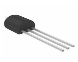
IRF730 Transistor: Datasheet, Pinout, IRF730 vs. IRF740


N-Channel Tube 1 Ω @ 3A, 10V ±20V 530pF @ 25V 24nC @ 10V TO-220-3
IRF730 is an N channel MOSFET available in TO-220 and TO-220AB packages. This post will show you more details about IRF730. There is a huge range of Semiconductors, Capacitors, Resistors and ICs in stock. Welcome RFQ.

Transistor IRF730
IRF730 Pinout

IRF730 Pinout


IRF730 Description
The IRF730 is an N channel MOSFET with TO-220 and TO-220AB packaging. This MOSFET can drive a load of up to 5.5A at 400V load voltage, with a maximum power dissipation of 75 Watts and a maximum pulse drain current of 22A.
IRF730 can also be used for audio amplification purposes and can be used to build high power audio amplifiers.
IRF730 Manufacturer
STMicroelectronics is a globally recognized semiconductor company. They are dedicated to developing semiconductor solutions for various microelectronics applications. STMicroelectronics enjoys unrivalled silicon and system expertise, strong manufacturing strength, IP portfolio, and solid relationships with their strategic partners. Based on these advantages, STMicroelectronics has become a pioneer in System-on-Chip (SoC) technology and its products have a positive effect in realizing today's convergence trends.
IRF730 Features
Package Type: TO-220AB And TO-220
Transistor Type: N Channel
Max Voltage Applied From Drain to Source: 400V
Max Gate to Source Voltage Should Be: ±20V
Max Continues Drain Current is: 5.5A
Max Pulsed Drain Current is: 22A
Max Power Dissipation is: 75W
Minimum Voltage Required to Conduct: 2V to 4V
Max Storage & Operating temperature Should Be: -55 to +150℃
IRF730 Application
IRF730 Equivalent
The equivalent for IRF730:
IRFS731
IRF730FI
IRF730S
IRFI730G
BUZ60
IRFS730
IRF330
IRF331
STP7NA40
Where & How to use IRF730?
The IRF730 can be used in high-voltage applications up to 400 volts. Aside from that, this transistor is suitable for a wide range of general-purpose applications. It can also be used at the outputs of ICs and microcontrollers to drive loads up to 5.5A, as well as at the outputs of electronic platforms like the Arduino and Raspberry Pi.


How to Make IRF730 Safely Long Run in a Circuit?
To get better and longer-lasting performance from an electronic component, the designer or user should not use it at its highest capability or ratings; instead, we recommend using it at least 20% below its maximum ratings. As a result, the same holds true for the IRF730: the transistor's maximum drain to source voltage is 400V, so don't drive loads higher than 320V; the transistor's maximum continuous current is 5.5A, so don't drive loads higher than 4.4A. Because the maximum pulsed drain current is 22A, never drive a load greater than 17.6A and always operate and store the transistor at temperatures between -55 and +150 ℃.
How to Package IRF730?

IRF730 Package
Parts with Similar Specs
Specifications
- TypeParameter
- Mount
In electronic components, the term "Mount" typically refers to the method or process of physically attaching or fixing a component onto a circuit board or other electronic device. This can involve soldering, adhesive bonding, or other techniques to secure the component in place. The mounting process is crucial for ensuring proper electrical connections and mechanical stability within the electronic system. Different components may have specific mounting requirements based on their size, shape, and function, and manufacturers provide guidelines for proper mounting procedures to ensure optimal performance and reliability of the electronic device.
Through Hole - Mounting Type
The "Mounting Type" in electronic components refers to the method used to attach or connect a component to a circuit board or other substrate, such as through-hole, surface-mount, or panel mount.
Through Hole - Package / Case
refers to the protective housing that encases an electronic component, providing mechanical support, electrical connections, and thermal management.
TO-220-3 - Number of Pins3
- Transistor Element Material
The "Transistor Element Material" parameter in electronic components refers to the material used to construct the transistor within the component. Transistors are semiconductor devices that amplify or switch electronic signals and are a fundamental building block in electronic circuits. The material used for the transistor element can significantly impact the performance and characteristics of the component. Common materials used for transistor elements include silicon, germanium, and gallium arsenide, each with its own unique properties and suitability for different applications. The choice of transistor element material is crucial in designing electronic components to meet specific performance requirements such as speed, power efficiency, and temperature tolerance.
SILICON - Current - Continuous Drain (Id) @ 25℃5.5A Tc
- Drive Voltage (Max Rds On, Min Rds On)10V
- Number of Elements1
- Power Dissipation (Max)100W Tc
- Turn Off Delay Time
It is the time from when Vgs drops below 90% of the gate drive voltage to when the drain current drops below 90% of the load current. It is the delay before current starts to transition in the load, and depends on Rg. Ciss.
15 ns - Operating Temperature
The operating temperature is the range of ambient temperature within which a power supply, or any other electrical equipment, operate in. This ranges from a minimum operating temperature, to a peak or maximum operating temperature, outside which, the power supply may fail.
150°C TJ - Packaging
Semiconductor package is a carrier / shell used to contain and cover one or more semiconductor components or integrated circuits. The material of the shell can be metal, plastic, glass or ceramic.
Tube - Series
In electronic components, the "Series" refers to a group of products that share similar characteristics, designs, or functionalities, often produced by the same manufacturer. These components within a series typically have common specifications but may vary in terms of voltage, power, or packaging to meet different application needs. The series name helps identify and differentiate between various product lines within a manufacturer's catalog.
PowerMESH™ II - JESD-609 Code
The "JESD-609 Code" in electronic components refers to a standardized marking code that indicates the lead-free solder composition and finish of electronic components for compliance with environmental regulations.
e3 - Part Status
Parts can have many statuses as they progress through the configuration, analysis, review, and approval stages.
Obsolete - Moisture Sensitivity Level (MSL)
Moisture Sensitivity Level (MSL) is a standardized rating that indicates the susceptibility of electronic components, particularly semiconductors, to moisture-induced damage during storage and the soldering process, defining the allowable exposure time to ambient conditions before they require special handling or baking to prevent failures
1 (Unlimited) - Number of Terminations3
- ECCN Code
An ECCN (Export Control Classification Number) is an alphanumeric code used by the U.S. Bureau of Industry and Security to identify and categorize electronic components and other dual-use items that may require an export license based on their technical characteristics and potential for military use.
EAR99 - Terminal Finish
Terminal Finish refers to the surface treatment applied to the terminals or leads of electronic components to enhance their performance and longevity. It can improve solderability, corrosion resistance, and overall reliability of the connection in electronic assemblies. Common finishes include nickel, gold, and tin, each possessing distinct properties suitable for various applications. The choice of terminal finish can significantly impact the durability and effectiveness of electronic devices.
Matte Tin (Sn) - Additional Feature
Any Feature, including a modified Existing Feature, that is not an Existing Feature.
HIGH VOLTAGE, FAST SWITCHING - Voltage - Rated DC
Voltage - Rated DC is a parameter that specifies the maximum direct current (DC) voltage that an electronic component can safely handle without being damaged. This rating is crucial for ensuring the proper functioning and longevity of the component in a circuit. Exceeding the rated DC voltage can lead to overheating, breakdown, or even permanent damage to the component. It is important to carefully consider this parameter when designing or selecting components for a circuit to prevent any potential issues related to voltage overload.
400V - Current Rating
Current rating is the maximum current that a fuse will carry for an indefinite period without too much deterioration of the fuse element.
5.5A - Base Part Number
The "Base Part Number" (BPN) in electronic components serves a similar purpose to the "Base Product Number." It refers to the primary identifier for a component that captures the essential characteristics shared by a group of similar components. The BPN provides a fundamental way to reference a family or series of components without specifying all the variations and specific details.
IRF7 - Pin Count
a count of all of the component leads (or pins)
3 - Voltage
Voltage is a measure of the electric potential difference between two points in an electrical circuit. It is typically represented by the symbol "V" and is measured in volts. Voltage is a crucial parameter in electronic components as it determines the flow of electric current through a circuit. It is responsible for driving the movement of electrons from one point to another, providing the energy needed for electronic devices to function properly. In summary, voltage is a fundamental concept in electronics that plays a key role in the operation and performance of electronic components.
400V - Element Configuration
The distribution of electrons of an atom or molecule (or other physical structure) in atomic or molecular orbitals.
Single - Current
In electronic components, "Current" refers to the flow of electric charge through a conductor or semiconductor material. It is measured in amperes (A) and represents the rate at which electric charge is moving past a specific point in a circuit. Current is a crucial parameter in electronics as it determines the amount of power being consumed or delivered by a component. Understanding and controlling current is essential for designing and operating electronic circuits efficiently and safely. In summary, current is a fundamental electrical quantity that plays a key role in the functionality and performance of electronic components.
55A - Operating Mode
A phase of operation during the operation and maintenance stages of the life cycle of a facility.
ENHANCEMENT MODE - Power Dissipation
the process by which an electronic or electrical device produces heat (energy loss or waste) as an undesirable derivative of its primary action.
100W - FET Type
"FET Type" refers to the type of Field-Effect Transistor (FET) being used in an electronic component. FETs are three-terminal semiconductor devices that can be classified into different types based on their construction and operation. The main types of FETs include Metal-Oxide-Semiconductor FETs (MOSFETs), Junction FETs (JFETs), and Insulated-Gate Bipolar Transistors (IGBTs).Each type of FET has its own unique characteristics and applications. MOSFETs are commonly used in digital circuits due to their high input impedance and low power consumption. JFETs are often used in low-noise amplifiers and switching circuits. IGBTs combine the high input impedance of MOSFETs with the high current-carrying capability of bipolar transistors, making them suitable for high-power applications like motor control and power inverters.When selecting an electronic component, understanding the FET type is crucial as it determines the device's performance and suitability for a specific application. It is important to consider factors such as voltage ratings, current handling capabilities, switching speeds, and power dissipation when choosing the right FET type for a particular circuit design.
N-Channel - Transistor Application
In the context of electronic components, the parameter "Transistor Application" refers to the specific purpose or function for which a transistor is designed and used. Transistors are semiconductor devices that can amplify or switch electronic signals and are commonly used in various electronic circuits. The application of a transistor can vary widely depending on its design and characteristics, such as whether it is intended for audio amplification, digital logic, power control, or radio frequency applications. Understanding the transistor application is important for selecting the right type of transistor for a particular circuit or system to ensure optimal performance and functionality.
SWITCHING - Rds On (Max) @ Id, Vgs
Rds On (Max) @ Id, Vgs refers to the maximum on-resistance of a MOSFET or similar transistor when it is fully turned on or in the saturation region. It is specified at a given drain current (Id) and gate-source voltage (Vgs). This parameter indicates how much resistance the component will offer when conducting, impacting power loss and efficiency in a circuit. Lower Rds On values are preferred for better performance in switching applications.
1 Ω @ 3A, 10V - Vgs(th) (Max) @ Id
The parameter "Vgs(th) (Max) @ Id" in electronic components refers to the maximum gate-source threshold voltage at a specified drain current (Id). This parameter is commonly found in field-effect transistors (FETs) and is used to define the minimum voltage required at the gate terminal to turn on the transistor and allow current to flow from the drain to the source. The maximum value indicates the upper limit of this threshold voltage under specified operating conditions. It is an important parameter for determining the proper biasing and operating conditions of the FET in a circuit to ensure proper functionality and performance.
4V @ 250μA - Input Capacitance (Ciss) (Max) @ Vds
The parameter "Input Capacitance (Ciss) (Max) @ Vds" in electronic components refers to the maximum input capacitance measured at a specific drain-source voltage (Vds). Input capacitance is a crucial parameter in field-effect transistors (FETs) and power MOSFETs, as it represents the total capacitance at the input terminal of the device. This capacitance affects the device's switching speed and overall performance, as it influences the time required for charging and discharging during operation. Manufacturers provide this parameter to help designers understand the device's input characteristics and make informed decisions when integrating it into a circuit.
530pF @ 25V - Gate Charge (Qg) (Max) @ Vgs
Gate Charge (Qg) (Max) @ Vgs refers to the maximum amount of charge that must be supplied to the gate of a MOSFET or similar device to fully turn it on, measured at a specific gate-source voltage (Vgs). This parameter is crucial for understanding the switching characteristics of the device, as it influences the speed at which the gate can charge and discharge. A higher gate charge value often implies slower switching speeds, which can impact the efficiency of high-frequency applications. This parameter is typically specified in nanocoulombs (nC) in the component's datasheet.
24nC @ 10V - Rise Time
In electronics, when describing a voltage or current step function, rise time is the time taken by a signal to change from a specified low value to a specified high value.
11ns - Vgs (Max)
Vgs (Max) refers to the maximum gate-source voltage that can be applied to a field-effect transistor (FET) without causing damage to the component. This parameter is crucial in determining the safe operating limits of the FET and helps prevent overvoltage conditions that could lead to device failure. Exceeding the specified Vgs (Max) rating can result in breakdown of the gate oxide layer, leading to permanent damage to the FET. Designers must ensure that the applied gate-source voltage does not exceed the maximum rating to ensure reliable and long-term operation of the electronic component.
±20V - Fall Time (Typ)
Fall Time (Typ) is a parameter used to describe the time it takes for a signal to transition from a high level to a low level in an electronic component, such as a transistor or an integrated circuit. It is typically measured in nanoseconds or microseconds and is an important characteristic that affects the performance of the component in digital circuits. A shorter fall time indicates faster switching speeds and can result in improved overall circuit performance, such as reduced power consumption and increased data transmission rates. Designers often consider the fall time specification when selecting components for their circuits to ensure proper functionality and efficiency.
9 ns - Continuous Drain Current (ID)
Continuous Drain Current (ID) is a key parameter in electronic components, particularly in field-effect transistors (FETs) such as MOSFETs. It refers to the maximum current that can flow continuously through the drain terminal of the FET without causing damage to the component. This parameter is crucial for determining the power handling capability of the FET and is specified by the manufacturer in the component's datasheet. Designers must ensure that the actual operating current does not exceed the specified Continuous Drain Current to prevent overheating and potential failure of the component.
5.5A - JEDEC-95 Code
JEDEC-95 Code is a standardized identification system used by the Joint Electron Device Engineering Council to categorize and describe semiconductor devices. This code provides a unique alphanumeric identifier for various memory components, ensuring consistency in documentation and communication across the electronics industry. The format includes information about the type, capacity, and technology of the device, facilitating easier specification and understanding for manufacturers and engineers.
TO-220AB - Gate to Source Voltage (Vgs)
The Gate to Source Voltage (Vgs) is a crucial parameter in electronic components, particularly in field-effect transistors (FETs) such as MOSFETs. It refers to the voltage difference between the gate and source terminals of the FET. This voltage determines the conductivity of the FET and controls the flow of current through the device. By varying the Vgs, the FET can be switched on or off, allowing for precise control of electronic circuits. Understanding and properly managing the Vgs is essential for ensuring the reliable and efficient operation of FET-based circuits.
20V - Drain-source On Resistance-Max
Drain-source On Resistance-Max, commonly referred to as RDS(on) max, is a specification for MOSFETs that indicates the maximum resistance between the drain and source terminals when the device is turned on. This parameter is critical for assessing the efficiency of a MOSFET in a circuit, as lower values result in reduced power loss and heat generation during operation. It is measured in ohms and is influenced by factors such as temperature and gate-to-source voltage. Understanding RDS(on) max is essential for optimizing performance in power management and switching applications.
1Ohm - Drain to Source Breakdown Voltage
Drain to Source Breakdown Voltage, often denoted as V(BR) D-S, is a critical parameter in electronic components, particularly in field-effect transistors (FETs) and metal-oxide-semiconductor FETs (MOSFETs). It represents the maximum voltage that can be applied between the drain and source terminals of the device without causing breakdown or permanent damage. Exceeding this voltage can lead to excessive current flow, resulting in thermal failure or destruction of the component. It is essential for ensuring reliable operation in circuit designs where high voltages may be encountered.
400V - Feedback Cap-Max (Crss)
Feedback Cap-Max (Crss) refers to the maximum capacitance between the output and input of an electronic component, such as a transistor or an operational amplifier. It indicates the level of feedback capacitance that can negatively affect the performance, stability, and bandwidth of the device. A higher Crss value may introduce unintended phase shifts or frequency response issues, making it crucial to consider in circuit design to ensure optimal operation.
65 pF - Radiation Hardening
Radiation hardening is the process of making electronic components and circuits resistant to damage or malfunction caused by high levels of ionizing radiation, especially for environments in outer space (especially beyond the low Earth orbit), around nuclear reactors and particle accelerators, or during nuclear accidents or nuclear warfare.
No - RoHS Status
RoHS means “Restriction of Certain Hazardous Substances” in the “Hazardous Substances Directive” in electrical and electronic equipment.
ROHS3 Compliant - Lead Free
Lead Free is a term used to describe electronic components that do not contain lead as part of their composition. Lead is a toxic material that can have harmful effects on human health and the environment, so the electronics industry has been moving towards lead-free components to reduce these risks. Lead-free components are typically made using alternative materials such as silver, copper, and tin. Manufacturers must comply with regulations such as the Restriction of Hazardous Substances (RoHS) directive to ensure that their products are lead-free and environmentally friendly.
Contains Lead
Datasheet PDF
- Datasheets :
Trend Analysis
What is IRF730?
The IRF730 is an N channel MOSFET with TO-220 and TO-220AB packaging. This MOSFET can drive a load of up to 5.5A at 400V load voltage, with a maximum power dissipation of 75 Watts and a maximum pulse drain current of 22A. IRF730 can also be used for audio amplification purposes and can be used to build high power audio amplifiers.
What is IRF730 designed for?
This MOSFET is primarily designed for high-speed switching applications, therefore it can be used in an uninterruptible power supply. It can also be utilized in DC to DC converters, telecommunications applications, lighting applications, and a variety of industrial applications. Because the IRF730 transistor has a low gate drive power need, it can be driven directly from the output of chips and electronic platforms.
What conditions does IRF730 operate?
Max Voltage Applied From Drain to Source: 400V Max Gate to Source Voltage Should Be: ±20V Max Continues Drain Current is: 5.5A Max Pulsed Drain Current is: 22A Max Power Dissipation is: 75W Minimum Voltage Required to Conduct: 2V to 4V Max Storage & Operating temperature Should Be: -55 to +150
 LTC6752IMS8-2#TRPBF Linear Comparator: Product Overview and Applications
06 March 2024241
 1N5819 Schottky Diode: Pinout, Datasheet, and Advantages
01 July 20217400
 UC3844 PWM Controller: Uses, Pinout and Datasheet
11 August 202114127
![ICL7660S Voltage Regulators DC Switching Regulators[Video]:Datasheet, Pinout, and Applications.](https://res.utmel.com/Images/Article/91a532a5-68a0-4d45-acb6-10f0b31c4052.png) ICL7660S Voltage Regulators DC Switching Regulators[Video]:Datasheet, Pinout, and Applications.
ICL7660S Voltage Regulators DC Switching Regulators[Video]:Datasheet, Pinout, and Applications.01 April 20222596
 AD595AQ vs AD595CQ: Thermocouple Amplifier Comparison
30 June 2025332
 STWD100NYWY3F: ST, Watchdog Timer Circuit, STWD100NYWY3F PDF
05 January 20221996
 BC183 Bipolar NPN Transistor: 30V, 01A, TO92, BC183 Transistor Pinout and Equivalent
12 January 20223010
 Designing with AD9850: Datasheet, Pinout, and Sine Wave Synthesis Guide
05 February 2026153
 An Overview of LPDDR
25 March 202633354
 What are Smart Sensors?
27 October 20252812
 What is a Semiconductor?
22 October 20257956
 What is a Monostable Multivibrator?
16 January 20216499
 What is a Ceramic Filter?
10 April 20214598
 How does an Inverter Work?
06 April 202110189
 Bearing: Features, Types and Uses
08 February 20229763
 Introduction to Flyback Transformer
29 January 202111603
STMicroelectronics
In Stock
United States
China
Canada
Japan
Russia
Germany
United Kingdom
Singapore
Italy
Hong Kong(China)
Taiwan(China)
France
Korea
Mexico
Netherlands
Malaysia
Austria
Spain
Switzerland
Poland
Thailand
Vietnam
India
United Arab Emirates
Afghanistan
Åland Islands
Albania
Algeria
American Samoa
Andorra
Angola
Anguilla
Antigua & Barbuda
Argentina
Armenia
Aruba
Australia
Azerbaijan
Bahamas
Bahrain
Bangladesh
Barbados
Belarus
Belgium
Belize
Benin
Bermuda
Bhutan
Bolivia
Bonaire, Sint Eustatius and Saba
Bosnia & Herzegovina
Botswana
Brazil
British Indian Ocean Territory
British Virgin Islands
Brunei
Bulgaria
Burkina Faso
Burundi
Cabo Verde
Cambodia
Cameroon
Cayman Islands
Central African Republic
Chad
Chile
Christmas Island
Cocos (Keeling) Islands
Colombia
Comoros
Congo
Congo (DRC)
Cook Islands
Costa Rica
Côte d’Ivoire
Croatia
Cuba
Curaçao
Cyprus
Czechia
Denmark
Djibouti
Dominica
Dominican Republic
Ecuador
Egypt
El Salvador
Equatorial Guinea
Eritrea
Estonia
Eswatini
Ethiopia
Falkland Islands
Faroe Islands
Fiji
Finland
French Guiana
French Polynesia
Gabon
Gambia
Georgia
Ghana
Gibraltar
Greece
Greenland
Grenada
Guadeloupe
Guam
Guatemala
Guernsey
Guinea
Guinea-Bissau
Guyana
Haiti
Honduras
Hungary
Iceland
Indonesia
Iran
Iraq
Ireland
Isle of Man
Israel
Jamaica
Jersey
Jordan
Kazakhstan
Kenya
Kiribati
Kosovo
Kuwait
Kyrgyzstan
Laos
Latvia
Lebanon
Lesotho
Liberia
Libya
Liechtenstein
Lithuania
Luxembourg
Macao(China)
Madagascar
Malawi
Maldives
Mali
Malta
Marshall Islands
Martinique
Mauritania
Mauritius
Mayotte
Micronesia
Moldova
Monaco
Mongolia
Montenegro
Montserrat
Morocco
Mozambique
Myanmar
Namibia
Nauru
Nepal
New Caledonia
New Zealand
Nicaragua
Niger
Nigeria
Niue
Norfolk Island
North Korea
North Macedonia
Northern Mariana Islands
Norway
Oman
Pakistan
Palau
Palestinian Authority
Panama
Papua New Guinea
Paraguay
Peru
Philippines
Pitcairn Islands
Portugal
Puerto Rico
Qatar
Réunion
Romania
Rwanda
Samoa
San Marino
São Tomé & Príncipe
Saudi Arabia
Senegal
Serbia
Seychelles
Sierra Leone
Sint Maarten
Slovakia
Slovenia
Solomon Islands
Somalia
South Africa
South Sudan
Sri Lanka
St Helena, Ascension, Tristan da Cunha
St. Barthélemy
St. Kitts & Nevis
St. Lucia
St. Martin
St. Pierre & Miquelon
St. Vincent & Grenadines
Sudan
Suriname
Svalbard & Jan Mayen
Sweden
Syria
Tajikistan
Tanzania
Timor-Leste
Togo
Tokelau
Tonga
Trinidad & Tobago
Tunisia
Turkey
Turkmenistan
Turks & Caicos Islands
Tuvalu
U.S. Outlying Islands
U.S. Virgin Islands
Uganda
Ukraine
Uruguay
Uzbekistan
Vanuatu
Vatican City
Venezuela
Wallis & Futuna
Yemen
Zambia
Zimbabwe
![STW9NK90Z]() STW9NK90Z
STW9NK90ZSTMicroelectronics
![STD20NF20]() STD20NF20
STD20NF20STMicroelectronics
![STP80NF10]() STP80NF10
STP80NF10STMicroelectronics
![STW9N150]() STW9N150
STW9N150STMicroelectronics
![STW11NK100Z]() STW11NK100Z
STW11NK100ZSTMicroelectronics
![STH3N150-2]() STH3N150-2
STH3N150-2STMicroelectronics
![STP12NM50FP]() STP12NM50FP
STP12NM50FPSTMicroelectronics
![STW45NM60]() STW45NM60
STW45NM60STMicroelectronics
![STP11NK50ZFP]() STP11NK50ZFP
STP11NK50ZFPSTMicroelectronics
![STP12NM50]() STP12NM50
STP12NM50STMicroelectronics


