
 Product
 Brand
Brand Articles
 Tools
Tools
LM139 Differential Comparator: Circuit, Pinout and Datasheet PDF

Surface Mount Tube 20mA mA 1.3 μs μs Linear Comparators 106.02dB dB 100nA pA 2mA μA 5mV mV Surface Mount


Surface Mount Tube 20mA mA 1.3 μs μs Linear Comparators 106.02dB dB 100nA pA 2mA μA 5mV mV Surface Mount
The LM139 device consists of four independent voltage comparators that are designed to operate from a single power supply over and a wide range of voltages. This article mainly introduce its circuit, pinout, datasheet PDF and other detailed information.

LM139 LM239 LM339 comparateur de tension voltage comparators
LM139 Description
The LM139 device consists of four independent voltage comparators that are designed to operate from a single power supply over and a wide range of voltages. Operation from dual supplies also is possible, as long as the difference between the two supplies is 2 V to 36 V, and VCC is at least 1.5 V more positive than the input common mode voltage. Current drain is independent of the supply voltage. The outputs can be connected to other open-collector outputs to achieve wired-AND relationships. The LM139 device is characterized for operation over the full military temperature range of –55°C to 125°C.
LM139 Pinout


LM139 CAD Model
Symbol

Footprint

3D Model

LM139 Features
• Wide Supply Ranges
– Single Supply: 2 V to 36 V
(Tested to 30 V for Non-V Devices and
32 V for V-Suffix Devices)
– Dual Supplies: ±1 V to ±18 V
(Tested to ±15 V for Non-V Devices and
±16 V for V-Suffix Devices)
• Low Supply-Current Drain Independent of
Supply Voltage: 0.8 mA (Typical)
• Low Input Bias Current: 25 nA (Typical)
• Low Input Offset Current: 3 nA (Typical) (LM139)
Low Input Offset Voltage: 2 mV (Typical)
Common-Mode Input Voltage Range
Includes Ground
• Differential Input Voltage Range Equal to
Maximum-Rated Supply Voltage: ±36 V
Low Output Saturation Voltage
Output Compatible With TTL, MOS, and CMOS
• On Products Compliant to MIL-PRF-38535,
All Parameters Are Tested Unless Otherwise
Noted. On All Other Products, Production
Processing Does Not Necessarily Include Testing
of All Parameters.
LM139 Package


LM139 Application
●Industrial
● Automotive
– HEV/EV and Power Trains
– Infotainment and Clusters
– Body Control Modules
● Power Supervision
● Oscillators
●Peak Detectors
● Logic Voltage Translation
Specifications
- TypeParameter
- Lifecycle Status
Lifecycle Status refers to the current stage of an electronic component in its product life cycle, indicating whether it is active, obsolete, or transitioning between these states. An active status means the component is in production and available for purchase. An obsolete status indicates that the component is no longer being manufactured or supported, and manufacturers typically provide a limited time frame for support. Understanding the lifecycle status is crucial for design engineers to ensure continuity and reliability in their projects.
ACTIVE (Last Updated: 5 days ago) - Factory Lead Time6 Weeks
- Mount
In electronic components, the term "Mount" typically refers to the method or process of physically attaching or fixing a component onto a circuit board or other electronic device. This can involve soldering, adhesive bonding, or other techniques to secure the component in place. The mounting process is crucial for ensuring proper electrical connections and mechanical stability within the electronic system. Different components may have specific mounting requirements based on their size, shape, and function, and manufacturers provide guidelines for proper mounting procedures to ensure optimal performance and reliability of the electronic device.
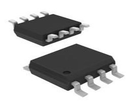
Surface Mount - Mounting Type
The "Mounting Type" in electronic components refers to the method used to attach or connect a component to a circuit board or other substrate, such as through-hole, surface-mount, or panel mount.
Surface Mount - Package / Case
refers to the protective housing that encases an electronic component, providing mechanical support, electrical connections, and thermal management.
14-SOIC (0.154, 3.90mm Width) - Number of Pins14
- Weight127.998097mg
- Number of Elements4
- Usage LevelMilitary grade
- Operating Temperature
The operating temperature is the range of ambient temperature within which a power supply, or any other electrical equipment, operate in. This ranges from a minimum operating temperature, to a peak or maximum operating temperature, outside which, the power supply may fail.
-55°C~125°C - Packaging
Semiconductor package is a carrier / shell used to contain and cover one or more semiconductor components or integrated circuits. The material of the shell can be metal, plastic, glass or ceramic.
Tube - JESD-609 Code
The "JESD-609 Code" in electronic components refers to a standardized marking code that indicates the lead-free solder composition and finish of electronic components for compliance with environmental regulations.
e4 - Pbfree Code
The "Pbfree Code" parameter in electronic components refers to the code or marking used to indicate that the component is lead-free. Lead (Pb) is a toxic substance that has been widely used in electronic components for many years, but due to environmental concerns, there has been a shift towards lead-free alternatives. The Pbfree Code helps manufacturers and users easily identify components that do not contain lead, ensuring compliance with regulations and promoting environmentally friendly practices. It is important to pay attention to the Pbfree Code when selecting electronic components to ensure they meet the necessary requirements for lead-free applications.
yes - Part Status
Parts can have many statuses as they progress through the configuration, analysis, review, and approval stages.
Active - Moisture Sensitivity Level (MSL)
Moisture Sensitivity Level (MSL) is a standardized rating that indicates the susceptibility of electronic components, particularly semiconductors, to moisture-induced damage during storage and the soldering process, defining the allowable exposure time to ambient conditions before they require special handling or baking to prevent failures
1 (Unlimited) - Number of Terminations14
- ECCN Code
An ECCN (Export Control Classification Number) is an alphanumeric code used by the U.S. Bureau of Industry and Security to identify and categorize electronic components and other dual-use items that may require an export license based on their technical characteristics and potential for military use.
EAR99 - TypeDifferential
- Terminal Finish
Terminal Finish refers to the surface treatment applied to the terminals or leads of electronic components to enhance their performance and longevity. It can improve solderability, corrosion resistance, and overall reliability of the connection in electronic assemblies. Common finishes include nickel, gold, and tin, each possessing distinct properties suitable for various applications. The choice of terminal finish can significantly impact the durability and effectiveness of electronic devices.
Nickel/Palladium/Gold (Ni/Pd/Au) - Packing Method
The packing method in electronic components refers to the technique used to package and protect the component during shipping and handling. It encompasses various forms including tape and reel, tray, tube, or bulk packaging, each suited for different types of components and manufacturing processes. The choice of packing method can affect the ease of handling, storage, and the efficiency of assembly in automated processes. Additionally, it plays a crucial role in ensuring the reliability and integrity of the components until they are used in electronic devices.
TR - Terminal Position
In electronic components, the term "Terminal Position" refers to the physical location of the connection points on the component where external electrical connections can be made. These connection points, known as terminals, are typically used to attach wires, leads, or other components to the main body of the electronic component. The terminal position is important for ensuring proper connectivity and functionality of the component within a circuit. It is often specified in technical datasheets or component specifications to help designers and engineers understand how to properly integrate the component into their circuit designs.
DUAL - Terminal Form
Occurring at or forming the end of a series, succession, or the like; closing; concluding.
GULL WING - Peak Reflow Temperature (Cel)
Peak Reflow Temperature (Cel) is a parameter that specifies the maximum temperature at which an electronic component can be exposed during the reflow soldering process. Reflow soldering is a common method used to attach electronic components to a circuit board. The Peak Reflow Temperature is crucial because it ensures that the component is not damaged or degraded during the soldering process. Exceeding the specified Peak Reflow Temperature can lead to issues such as component failure, reduced performance, or even permanent damage to the component. It is important for manufacturers and assemblers to adhere to the recommended Peak Reflow Temperature to ensure the reliability and functionality of the electronic components.
260 - Number of Functions4
- Supply Voltage
Supply voltage refers to the electrical potential difference provided to an electronic component or circuit. It is crucial for the proper operation of devices, as it powers their functions and determines performance characteristics. The supply voltage must be within specified limits to ensure reliability and prevent damage to components. Different electronic devices have specific supply voltage requirements, which can vary widely depending on their design and intended application.
5V - Terminal Pitch
The center distance from one pole to the next.
1.27mm - Base Part Number
The "Base Part Number" (BPN) in electronic components serves a similar purpose to the "Base Product Number." It refers to the primary identifier for a component that captures the essential characteristics shared by a group of similar components. The BPN provides a fundamental way to reference a family or series of components without specifying all the variations and specific details.
LM139 - Pin Count
a count of all of the component leads (or pins)
14 - Output Type
The "Output Type" parameter in electronic components refers to the type of signal or data that is produced by the component as an output. This parameter specifies the nature of the output signal, such as analog or digital, and can also include details about the voltage levels, current levels, frequency, and other characteristics of the output signal. Understanding the output type of a component is crucial for ensuring compatibility with other components in a circuit or system, as well as for determining how the output signal can be utilized or processed further. In summary, the output type parameter provides essential information about the nature of the signal that is generated by the electronic component as its output.
CMOS, MOS, Open-Collector, TTL - Operating Supply Voltage
The voltage level by which an electrical system is designated and to which certain operating characteristics of the system are related.
3V - Power Supplies
an electronic circuit that converts the voltage of an alternating current (AC) into a direct current (DC) voltage.?
5V - Number of Circuits4
- Nominal Supply Current
Nominal current is the same as the rated current. It is the current drawn by the motor while delivering rated mechanical output at its shaft.
2mA - Output Current
The rated output current is the maximum load current that a power supply can provide at a specified ambient temperature. A power supply can never provide more current that it's rated output current unless there is a fault, such as short circuit at the load.
20mA - Max Supply Current
Max Supply Current refers to the maximum amount of electrical current that a component can draw from its power supply under normal operating conditions. It is a critical parameter that ensures the component operates reliably without exceeding its thermal limits or damaging internal circuitry. Exceeding this current can lead to overheating, performance degradation, or failure of the component. Understanding this parameter is essential for designing circuits that provide adequate power while avoiding overload situations.
500μA - Quiescent Current
The quiescent current is defined as the current level in the amplifier when it is producing an output of zero.
2mA - Response Time
the time taken for a circuit or measuring device, when subjected to a change in input signal, to change its state by a specified fraction of its total response to that change.
1.3 μs - Voltage - Supply, Single/Dual (±)
The parameter "Voltage - Supply, Single/Dual (±)" in electronic components refers to the power supply voltage required for the proper operation of the component. This parameter indicates whether the component requires a single power supply voltage (e.g., 5V) or a dual power supply voltage (e.g., ±15V). For components that require a single power supply voltage, only one voltage level is needed for operation. On the other hand, components that require a dual power supply voltage need both positive and negative voltage levels to function correctly.Understanding the voltage supply requirements of electronic components is crucial for designing and integrating them into circuits to ensure proper functionality and prevent damage due to incorrect voltage levels.
2V~30V ±1V~15V - Output Current per Channel
Output Current per Channel is a specification commonly found in electronic components such as amplifiers, audio interfaces, and power supplies. It refers to the maximum amount of electrical current that can be delivered by each individual output channel of the component. This parameter is important because it determines the capacity of the component to drive connected devices or loads. A higher output current per channel means the component can deliver more power to connected devices, while a lower output current may limit the performance or functionality of the component in certain applications. It is crucial to consider the output current per channel when selecting electronic components to ensure they can meet the power requirements of the intended system or setup.
6mA - Input Offset Voltage (Vos)
Input Offset Voltage (Vos) is a key parameter in electronic components, particularly in operational amplifiers. It refers to the voltage difference that must be applied between the two input terminals of the amplifier to nullify the output voltage when the input terminals are shorted together. In simpler terms, it represents the voltage required to bring the output of the amplifier to zero when there is no input signal present. Vos is an important parameter as it can introduce errors in the output signal of the amplifier, especially in precision applications where accuracy is crucial. Minimizing Vos is essential to ensure the amplifier operates with high precision and accuracy.
5mV - Voltage Gain
Voltage gain is a measure of how much an electronic component or circuit amplifies an input voltage signal to produce an output voltage signal. It is typically expressed as a ratio or in decibels (dB). A higher voltage gain indicates a greater amplification of the input signal. Voltage gain is an important parameter in amplifiers, where it determines the level of amplification provided by the circuit. It is calculated by dividing the output voltage by the input voltage and is a key factor in determining the overall performance and functionality of electronic devices.
106.02dB - Average Bias Current-Max (IIB)
The parameter "Average Bias Current-Max (IIB)" in electronic components refers to the maximum average bias current that the component can handle without exceeding its specified operating limits. Bias current is the current that flows through a component when it is in its quiescent state or when it is not actively processing a signal. Exceeding the maximum average bias current can lead to overheating, reduced performance, or even damage to the component. Therefore, it is important to ensure that the bias current does not exceed the specified maximum value to maintain the reliability and longevity of the electronic component.
0.025μA - Supply Voltage Limit-Max
The parameter "Supply Voltage Limit-Max" in electronic components refers to the maximum voltage that the component can safely handle without getting damaged. This specification is crucial for ensuring the reliable operation and longevity of the component within a given electrical system. Exceeding the maximum supply voltage limit can lead to overheating, electrical breakdown, or permanent damage to the component. It is important to carefully adhere to this limit when designing and operating electronic circuits to prevent potential failures and ensure the overall system's performance and safety.
36V - Max Input Current
Max Input Current is a parameter that specifies the maximum amount of electrical current that can safely flow into an electronic component without causing damage. It is an important consideration when designing or using electronic circuits to ensure that the component operates within its specified limits. Exceeding the maximum input current can lead to overheating, component failure, or even pose safety risks. Manufacturers provide this parameter in datasheets to help engineers and users understand the limitations of the component and ensure proper operation within the specified parameters.
100nA - Dual Supply Voltage
Dual Supply Voltage refers to an electronic component's requirement for two separate power supply voltages, typically one positive and one negative. This configuration is commonly used in operational amplifiers, analog circuits, and certain digital devices to allow for greater signal handling capabilities and improved performance. The use of dual supply voltages enables the device to process bipolar signals, thereby enhancing its functionality in various applications.
3V - Input Bias Current
Input Bias Current refers to the small amount of current that flows into the input terminals of an electronic component, such as an operational amplifier. It is primarily caused by the input impedance of the device and the characteristics of the transistors within it. This current is crucial in determining the accuracy of the analog signal processing, as it can affect the level of voltage offset and signal integrity in the application. In many precise applications, minimizing input bias current is essential to achieve optimal performance.
100nA - Voltage - Input Offset (Max)
Voltage - Input Offset (Max) is a parameter that refers to the maximum allowable difference in input voltage between two input terminals of an electronic component, such as an operational amplifier, before the output voltage deviates from the expected value. This parameter is crucial in precision applications where accurate voltage amplification or signal processing is required. A higher value for the input offset voltage indicates a greater potential for error in the output signal, so minimizing this parameter is important for maintaining the accuracy and reliability of the component's performance. Designers often take this parameter into consideration when selecting components for circuits that require precise voltage control and signal processing.
5mV @ 30V - Current - Input Bias (Max)
The parameter "Current - Input Bias (Max)" in electronic components refers to the maximum amount of input bias current that can flow into the input terminal of the component without causing any adverse effects on its performance. Input bias current is the small amount of current that flows into the input terminal of an electronic component, such as an operational amplifier, transistor, or integrated circuit, even when no input signal is applied. This parameter is important because excessive input bias current can lead to errors in the output signal and affect the overall performance of the component. Manufacturers specify a maximum value for input bias current to ensure proper operation and reliability of the component in various applications. It is crucial for designers and engineers to consider this parameter when selecting components for their circuits to ensure optimal performance and functionality.
0.1μA @ 5V - Height1.75mm
- Length8.65mm
- Width3.91mm
- Thickness
Thickness in electronic components refers to the measurement of how thick a particular material or layer is within the component structure. It can pertain to various aspects, such as the thickness of a substrate, a dielectric layer, or conductive traces. This parameter is crucial as it impacts the electrical, mechanical, and thermal properties of the component, influencing its performance and reliability in electronic circuits.
1.58mm - REACH SVHC
The parameter "REACH SVHC" in electronic components refers to the compliance with the Registration, Evaluation, Authorization, and Restriction of Chemicals (REACH) regulation regarding Substances of Very High Concern (SVHC). SVHCs are substances that may have serious effects on human health or the environment, and their use is regulated under REACH to ensure their safe handling and minimize their impact.Manufacturers of electronic components need to declare if their products contain any SVHCs above a certain threshold concentration and provide information on the safe use of these substances. This information allows customers to make informed decisions about the potential risks associated with using the components and take appropriate measures to mitigate any hazards.Ensuring compliance with REACH SVHC requirements is essential for electronics manufacturers to meet regulatory standards, protect human health and the environment, and maintain transparency in their supply chain. It also demonstrates a commitment to sustainability and responsible manufacturing practices in the electronics industry.
No SVHC - Radiation Hardening
Radiation hardening is the process of making electronic components and circuits resistant to damage or malfunction caused by high levels of ionizing radiation, especially for environments in outer space (especially beyond the low Earth orbit), around nuclear reactors and particle accelerators, or during nuclear accidents or nuclear warfare.
No - RoHS Status
RoHS means “Restriction of Certain Hazardous Substances” in the “Hazardous Substances Directive” in electrical and electronic equipment.
ROHS3 Compliant - Lead Free
Lead Free is a term used to describe electronic components that do not contain lead as part of their composition. Lead is a toxic material that can have harmful effects on human health and the environment, so the electronics industry has been moving towards lead-free components to reduce these risks. Lead-free components are typically made using alternative materials such as silver, copper, and tin. Manufacturers must comply with regulations such as the Restriction of Hazardous Substances (RoHS) directive to ensure that their products are lead-free and environmentally friendly.
Lead Free
LM139 Functional Block Diagram

Schematic (Each Comparator)
LM139 Typical Appplication


Basic Comparator Driving CMO Driving TTL


Low frequency op amp Low frequency op amp Transducer amplifier

Time delay generator


Low frequency op amp with offset Zero crossing detector Two-decade high-frequency VCO


Limit comparator Crystal-controlled oscillator


Comparator with a negative reference Zero crossing detector
LM139 Simplified Schematic

LM139 Layout Example

LM139 Manufacturer
As a global semiconductor company operating in 35 countries, Texas Instruments (TI) is first and foremost a reflection of its people. From the TIer who unveiled the first working integrated circuit in 1958 to the more than 30,000 TIers around the world today who design, manufacture and sell analog and embedded processing chips, we are problem-solvers collaborating to change the world through technology.
Trend Analysis
Datasheet PDF
- Datasheets :
- PCN Assembly/Origin :
- PCN Design/Specification :
1.What is the threshold voltage of LM139? Does it change according to the voltage applied across it?
LM139 is a 4 comparator, the output voltage is the comparison result of the voltage of the two input terminals, and the output is high when +input>-input. The threshold voltage isn't a matter, it is set by yourself.
2.What’s the difference between LM139 and TL074?
LM139 is a comparator, while TL074 is an operational amplifier.
3.What is the difference between lm139 suffix with j and aj?
The j after LM139j is the package symbol, and j stands for low-temperature glass dual in-line package. LM139aj, aj stands for advanced low temperature glass dual in-line package.
4.What is the difference between LM139 and LF444? Can be interchanged?
LM139 is a four-comparator, and LF444 is a four-op amp, and the order of their pins is different.
5.What is LM139 used to compare?
It is used to compare the input voltage of the positive and negative input terminals, and its output is an open-collector output.Therefore, to output high and low levels, a pull-up resistor must be pulled between the output terminal and the positive power supply.
6.My LM139 is broken, can I replace it with LM339?
The IC parameters of LM139 and LM339 are basically the same, and they can be used interchangeably in the COMS circuit.
 MAX232 Driver IC: Datasheet, Pinout and Circuit
10 September 20217698
 A1302 Hall Effect Sensor: Allegro A1302, Datasheet, A1302 Arduino
22 December 20218145
 OP249 Dual Op-Amp: Pinout, Applications and Datasheet
10 December 20211919
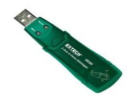 VB300 3-Axis G-Force Datalogger:Battery Replacement, Features and Application
08 January 20221242
 H6 vs H7 Battery: Which One Do You Like Better?
01 April 202249684
 LM2902N Low-power quad operational amplifier:Pinout, Features, and Datasheet
13 September 20212570
 How to use BME280 with Arduino?
07 June 20223860
 74HC04 Hex Inverter: Pinout, Circuit and Datasheet
24 August 202118623
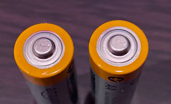 A Complete Guide to 2025 Battery vs 2032 Swapping
29 August 20254419
 NOR Flash: Working, Structure and Applications
18 November 202114240
 What is Mini LED?
08 December 20206319
 7 Common Functions of MOSFET Gate Circuits
22 January 20227383
 What is Field Programmable Gate Array?
29 September 20203790
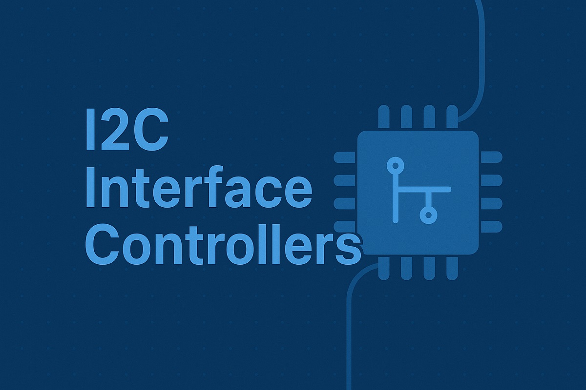 Understanding the Basics of I2C Interface Controllers
11 June 20251631
 Chip Filters, Piezoelectric Materials and the Piezoelectric Effect
27 September 20226908
 Difference between Various Motors and How to Select a Motor?
10 January 20224831
Texas Instruments
In Stock: 24
United States
China
Canada
Japan
Russia
Germany
United Kingdom
Singapore
Italy
Hong Kong(China)
Taiwan(China)
France
Korea
Mexico
Netherlands
Malaysia
Austria
Spain
Switzerland
Poland
Thailand
Vietnam
India
United Arab Emirates
Afghanistan
Åland Islands
Albania
Algeria
American Samoa
Andorra
Angola
Anguilla
Antigua & Barbuda
Argentina
Armenia
Aruba
Australia
Azerbaijan
Bahamas
Bahrain
Bangladesh
Barbados
Belarus
Belgium
Belize
Benin
Bermuda
Bhutan
Bolivia
Bonaire, Sint Eustatius and Saba
Bosnia & Herzegovina
Botswana
Brazil
British Indian Ocean Territory
British Virgin Islands
Brunei
Bulgaria
Burkina Faso
Burundi
Cabo Verde
Cambodia
Cameroon
Cayman Islands
Central African Republic
Chad
Chile
Christmas Island
Cocos (Keeling) Islands
Colombia
Comoros
Congo
Congo (DRC)
Cook Islands
Costa Rica
Côte d’Ivoire
Croatia
Cuba
Curaçao
Cyprus
Czechia
Denmark
Djibouti
Dominica
Dominican Republic
Ecuador
Egypt
El Salvador
Equatorial Guinea
Eritrea
Estonia
Eswatini
Ethiopia
Falkland Islands
Faroe Islands
Fiji
Finland
French Guiana
French Polynesia
Gabon
Gambia
Georgia
Ghana
Gibraltar
Greece
Greenland
Grenada
Guadeloupe
Guam
Guatemala
Guernsey
Guinea
Guinea-Bissau
Guyana
Haiti
Honduras
Hungary
Iceland
Indonesia
Iran
Iraq
Ireland
Isle of Man
Israel
Jamaica
Jersey
Jordan
Kazakhstan
Kenya
Kiribati
Kosovo
Kuwait
Kyrgyzstan
Laos
Latvia
Lebanon
Lesotho
Liberia
Libya
Liechtenstein
Lithuania
Luxembourg
Macao(China)
Madagascar
Malawi
Maldives
Mali
Malta
Marshall Islands
Martinique
Mauritania
Mauritius
Mayotte
Micronesia
Moldova
Monaco
Mongolia
Montenegro
Montserrat
Morocco
Mozambique
Myanmar
Namibia
Nauru
Nepal
New Caledonia
New Zealand
Nicaragua
Niger
Nigeria
Niue
Norfolk Island
North Korea
North Macedonia
Northern Mariana Islands
Norway
Oman
Pakistan
Palau
Palestinian Authority
Panama
Papua New Guinea
Paraguay
Peru
Philippines
Pitcairn Islands
Portugal
Puerto Rico
Qatar
Réunion
Romania
Rwanda
Samoa
San Marino
São Tomé & Príncipe
Saudi Arabia
Senegal
Serbia
Seychelles
Sierra Leone
Sint Maarten
Slovakia
Slovenia
Solomon Islands
Somalia
South Africa
South Sudan
Sri Lanka
St Helena, Ascension, Tristan da Cunha
St. Barthélemy
St. Kitts & Nevis
St. Lucia
St. Martin
St. Pierre & Miquelon
St. Vincent & Grenadines
Sudan
Suriname
Svalbard & Jan Mayen
Sweden
Syria
Tajikistan
Tanzania
Timor-Leste
Togo
Tokelau
Tonga
Trinidad & Tobago
Tunisia
Turkey
Turkmenistan
Turks & Caicos Islands
Tuvalu
U.S. Outlying Islands
U.S. Virgin Islands
Uganda
Ukraine
Uruguay
Uzbekistan
Vanuatu
Vatican City
Venezuela
Wallis & Futuna
Yemen
Zambia
Zimbabwe
![LMC7225IM5X]() LMC7225IM5X
LMC7225IM5XTexas Instruments
![LM393ADR]() LM393ADR
LM393ADRTexas Instruments
![LM339DR]() LM339DR
LM339DRTexas Instruments
![LM393DR]() LM393DR
LM393DRTexas Instruments
![LM311DR]() LM311DR
LM311DRTexas Instruments
![LM311P]() LM311P
LM311PTexas Instruments
![LM311M/NOPB]() LM311M/NOPB
LM311M/NOPBTexas Instruments
![LM239DR]() LM239DR
LM239DRTexas Instruments
![LM293ADR]() LM293ADR
LM293ADRTexas Instruments
![LM2903DGKR]() LM2903DGKR
LM2903DGKRTexas Instruments


