
 Product
 Brand
Brand Articles
 Tools
Tools
LM339S Quad Comparator: Pinout, Applications and Datasheet

Tube 16mA mA 1000 ns μs Linear Comparators 100dB dB 250nA pA 2002 5mV mV Through Hole
Unit Price: $0.988558
Ext Price: $0.99


Tube 16mA mA 1000 ns μs Linear Comparators 100dB dB 250nA pA 2002 5mV mV Through Hole
The LM339S Single Supply Quad comparator is designed for use in level detection, low−level sensing and memory applications in consumer and industrial electronic applications. Furthermore, Huge range of Semiconductors, Capacitors, Resistors and IcS in stock. Welcome RFQ.

Let's talk about comparators
LM339S Pinout

Pinout
LM339S CAD Model

Footprint

3D Model
LM339S Overview
The LM339S Single Supply Quad Comparator is designed for use in level detection, low−level sensing and memory applications in consumer and industrial electronic applications. These quad comparators feature high gain, wide bandwidth characteristics. This gives the device oscillation tendencies if the outputs are capacitively coupled to the inputs via stray capacitance.
This article provides you with a basic overview of the LM339S Single Supply Quad Comparator, including its pin descriptions, features and specifications, etc., to help you quickly understand what LM339S is.
LM339S Features
● Single or Split Supply Operation
● Low Input Bias Current: 25 nA (Typ)
● Low Input Offset Current: ±5.0 nA (Typ)
● Low Input Offset Voltage
● Input Common Mode Voltage Range to GND
● Low Output Saturation Voltage: 130 mV (Typ) @ 4.0 mA
● TTL and CMOS Compatible
● The Device is Pb−Free, Halogen Free/BFR Free and are RoHS Compliant
Specifications
- TypeParameter
- Lifecycle Status
Lifecycle Status refers to the current stage of an electronic component in its product life cycle, indicating whether it is active, obsolete, or transitioning between these states. An active status means the component is in production and available for purchase. An obsolete status indicates that the component is no longer being manufactured or supported, and manufacturers typically provide a limited time frame for support. Understanding the lifecycle status is crucial for design engineers to ensure continuity and reliability in their projects.
LAST SHIPMENTS (Last Updated: 1 day ago) - Factory Lead Time4 Weeks
- Mount
In electronic components, the term "Mount" typically refers to the method or process of physically attaching or fixing a component onto a circuit board or other electronic device. This can involve soldering, adhesive bonding, or other techniques to secure the component in place. The mounting process is crucial for ensuring proper electrical connections and mechanical stability within the electronic system. Different components may have specific mounting requirements based on their size, shape, and function, and manufacturers provide guidelines for proper mounting procedures to ensure optimal performance and reliability of the electronic device.
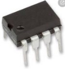
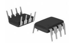
Through Hole - Package / Case
refers to the protective housing that encases an electronic component, providing mechanical support, electrical connections, and thermal management.
DIP - Number of Pins14
- Number of Elements4
- Usage LevelCommercial grade
- Packaging
Semiconductor package is a carrier / shell used to contain and cover one or more semiconductor components or integrated circuits. The material of the shell can be metal, plastic, glass or ceramic.
Tube - Published2002
- JESD-609 Code
The "JESD-609 Code" in electronic components refers to a standardized marking code that indicates the lead-free solder composition and finish of electronic components for compliance with environmental regulations.
e3 - Pbfree Code
The "Pbfree Code" parameter in electronic components refers to the code or marking used to indicate that the component is lead-free. Lead (Pb) is a toxic substance that has been widely used in electronic components for many years, but due to environmental concerns, there has been a shift towards lead-free alternatives. The Pbfree Code helps manufacturers and users easily identify components that do not contain lead, ensuring compliance with regulations and promoting environmentally friendly practices. It is important to pay attention to the Pbfree Code when selecting electronic components to ensure they meet the necessary requirements for lead-free applications.
yes - Part Status
Parts can have many statuses as they progress through the configuration, analysis, review, and approval stages.
Obsolete - Moisture Sensitivity Level (MSL)
Moisture Sensitivity Level (MSL) is a standardized rating that indicates the susceptibility of electronic components, particularly semiconductors, to moisture-induced damage during storage and the soldering process, defining the allowable exposure time to ambient conditions before they require special handling or baking to prevent failures
1 (Unlimited) - Number of Terminations14
- TypeGeneral Purpose
- Terminal Finish
Terminal Finish refers to the surface treatment applied to the terminals or leads of electronic components to enhance their performance and longevity. It can improve solderability, corrosion resistance, and overall reliability of the connection in electronic assemblies. Common finishes include nickel, gold, and tin, each possessing distinct properties suitable for various applications. The choice of terminal finish can significantly impact the durability and effectiveness of electronic devices.
Tin (Sn) - Max Operating Temperature
The Maximum Operating Temperature is the maximum body temperature at which the thermistor is designed to operate for extended periods of time with acceptable stability of its electrical characteristics.
70°C - Min Operating Temperature
The "Min Operating Temperature" parameter in electronic components refers to the lowest temperature at which the component is designed to operate effectively and reliably. This parameter is crucial for ensuring the proper functioning and longevity of the component, as operating below this temperature may lead to performance issues or even damage. Manufacturers specify the minimum operating temperature to provide guidance to users on the environmental conditions in which the component can safely operate. It is important to adhere to this parameter to prevent malfunctions and ensure the overall reliability of the electronic system.
0°C - Terminal Position
In electronic components, the term "Terminal Position" refers to the physical location of the connection points on the component where external electrical connections can be made. These connection points, known as terminals, are typically used to attach wires, leads, or other components to the main body of the electronic component. The terminal position is important for ensuring proper connectivity and functionality of the component within a circuit. It is often specified in technical datasheets or component specifications to help designers and engineers understand how to properly integrate the component into their circuit designs.
DUAL - Terminal Form
Occurring at or forming the end of a series, succession, or the like; closing; concluding.
PIN/PEG - Number of Functions4
- Supply Voltage
Supply voltage refers to the electrical potential difference provided to an electronic component or circuit. It is crucial for the proper operation of devices, as it powers their functions and determines performance characteristics. The supply voltage must be within specified limits to ensure reliability and prevent damage to components. Different electronic devices have specific supply voltage requirements, which can vary widely depending on their design and intended application.
5V - Qualification Status
An indicator of formal certification of qualifications.
Not Qualified - Output Type
The "Output Type" parameter in electronic components refers to the type of signal or data that is produced by the component as an output. This parameter specifies the nature of the output signal, such as analog or digital, and can also include details about the voltage levels, current levels, frequency, and other characteristics of the output signal. Understanding the output type of a component is crucial for ensuring compatibility with other components in a circuit or system, as well as for determining how the output signal can be utilized or processed further. In summary, the output type parameter provides essential information about the nature of the signal that is generated by the electronic component as its output.
TTL - Power Supplies
an electronic circuit that converts the voltage of an alternating current (AC) into a direct current (DC) voltage.?
5V - Temperature Grade
Temperature grades represent a tire's resistance to heat and its ability to dissipate heat when tested under controlled laboratory test conditions.
COMMERCIAL - Max Supply Voltage
In general, the absolute maximum common-mode voltage is VEE-0.3V and VCC+0.3V, but for products without a protection element at the VCC side, voltages up to the absolute maximum rated supply voltage (i.e. VEE+36V) can be supplied, regardless of supply voltage.
36V - Output Current
The rated output current is the maximum load current that a power supply can provide at a specified ambient temperature. A power supply can never provide more current that it's rated output current unless there is a fault, such as short circuit at the load.
16mA - Quiescent Current
The quiescent current is defined as the current level in the amplifier when it is producing an output of zero.
2.5mA - Response Time
the time taken for a circuit or measuring device, when subjected to a change in input signal, to change its state by a specified fraction of its total response to that change.
1000 ns - Input Offset Voltage (Vos)
Input Offset Voltage (Vos) is a key parameter in electronic components, particularly in operational amplifiers. It refers to the voltage difference that must be applied between the two input terminals of the amplifier to nullify the output voltage when the input terminals are shorted together. In simpler terms, it represents the voltage required to bring the output of the amplifier to zero when there is no input signal present. Vos is an important parameter as it can introduce errors in the output signal of the amplifier, especially in precision applications where accuracy is crucial. Minimizing Vos is essential to ensure the amplifier operates with high precision and accuracy.
5mV - Voltage Gain
Voltage gain is a measure of how much an electronic component or circuit amplifies an input voltage signal to produce an output voltage signal. It is typically expressed as a ratio or in decibels (dB). A higher voltage gain indicates a greater amplification of the input signal. Voltage gain is an important parameter in amplifiers, where it determines the level of amplification provided by the circuit. It is calculated by dividing the output voltage by the input voltage and is a key factor in determining the overall performance and functionality of electronic devices.
100dB - Average Bias Current-Max (IIB)
The parameter "Average Bias Current-Max (IIB)" in electronic components refers to the maximum average bias current that the component can handle without exceeding its specified operating limits. Bias current is the current that flows through a component when it is in its quiescent state or when it is not actively processing a signal. Exceeding the maximum average bias current can lead to overheating, reduced performance, or even damage to the component. Therefore, it is important to ensure that the bias current does not exceed the specified maximum value to maintain the reliability and longevity of the electronic component.
0.25μA - Max Dual Supply Voltage
A Dual power supply is a regular direct current power supply. It can provide a positive as well as negative voltage. It ensures stable power supply to the device as well as it helps to prevent system damage.
18V - Bias Current-Max (IIB) @25C
The parameter "Bias Current-Max (IIB) @25C" in electronic components refers to the maximum input bias current that the component can handle at a specified temperature of 25 degrees Celsius. Bias current is the current flowing into the input terminal of a device when no signal is applied. This parameter is important because excessive bias current can affect the performance and stability of the component, leading to potential issues such as distortion or offset errors in the output signal. By specifying the maximum bias current allowed at a certain temperature, manufacturers provide users with important information to ensure proper operation and reliability of the component in their circuit designs.
0.25μA - Input Bias Current
Input Bias Current refers to the small amount of current that flows into the input terminals of an electronic component, such as an operational amplifier. It is primarily caused by the input impedance of the device and the characteristics of the transistors within it. This current is crucial in determining the accuracy of the analog signal processing, as it can affect the level of voltage offset and signal integrity in the application. In many precise applications, minimizing input bias current is essential to achieve optimal performance.
250nA - Length19.18mm
- Height Seated (Max)
Height Seated (Max) is a parameter in electronic components that refers to the maximum allowable height of the component when it is properly seated or installed on a circuit board or within an enclosure. This specification is crucial for ensuring proper fit and alignment within the overall system design. Exceeding the maximum seated height can lead to mechanical interference, electrical shorts, or other issues that may impact the performance and reliability of the electronic device. Manufacturers provide this information to help designers and engineers select components that will fit within the designated space and function correctly in the intended application.
5.33mm - Width7.62mm
- RoHS Status
RoHS means “Restriction of Certain Hazardous Substances” in the “Hazardous Substances Directive” in electrical and electronic equipment.
RoHS Compliant - Lead Free
Lead Free is a term used to describe electronic components that do not contain lead as part of their composition. Lead is a toxic material that can have harmful effects on human health and the environment, so the electronics industry has been moving towards lead-free components to reduce these risks. Lead-free components are typically made using alternative materials such as silver, copper, and tin. Manufacturers must comply with regulations such as the Restriction of Hazardous Substances (RoHS) directive to ensure that their products are lead-free and environmentally friendly.
Lead Free
LM339S Functional Block Diagram

Circuit Schematic
Parts with Similar Specs
- ImagePart NumberManufacturerPackage / CaseNumber of PinsInput Offset Voltage (Vos)Max Dual Supply VoltageMax Supply VoltageSupply VoltageVoltage GainNumber of FunctionsView Compare
![LM339SNG]()
LM339SNG
DIP
14
5 mV
18 V
36 V
5 V
100 dB
4
![LM2901SNG]()
14-DIP (0.300, 7.62mm)
14
7 mV
18 V
36 V
5 V
100 dB
4

LM339S Applications
.png")
Zero Crossing Detector (Single Supply)
.png")
Zero Crossing Detector (Split Supplies)
LM339S Package

Top View

Side View

End View

End View

PDIP−14 package
LM339S Manufacturer
On Semiconductor (Nasdaq: ON) is a manufacturer engaging itself in reducing energy use. It features a comprehensive portfolio of power, signal management, and logic, custom solutions that are energy efficient. It acts as a world-class supply chain with high reliability and a network of manufacturing facilities, sales, offices, and design centers in key markets through North America, Europe, and the Asia Pacific regions.
Datasheet PDF
- PCN Obsolescence/ EOL :
- ReachStatement :
- Datasheets :
Trend Analysis
What is the essential property of the LM339S?
The LM339S Single Supply Quad comparator is designed for use in level detection, low−level sensing and memory applications in consumer and industrial electronic applications.
Will the LM339S device show a tendency to oscillate?
These quad comparators feature high gain, wide bandwidth characteristics. This gives the device oscillation tendencies if the outputs are capacitively coupled to the inputs via stray capacitance.
 PCF8575 I/O Expander : Pinout, Schematic and Datasheet
19 August 20219437
 Unveiling the SANYO LC87F5R96B 8-Bit Microcontroller: An In-depth Exploration
29 February 2024119
 MIC2042 High-side MOSFET Switch: Pinout, Equivalent and Datasheet
01 April 2022580
 LM258P Low Power Dual Bipolar Op-amps:Description,Features and Applications
25 February 20221650
 UPD78F0730 MCCAB-AX: Microcontroller Datasheet Overview
29 February 2024153
 dsPIC30F Acoustic Echo Cancellation (AEC) Library: Comprehensive Analysis
29 February 2024234
 TC4420 MOSFET Driver: Datasheet, Pinout, Application Circuit
13 December 202113973
 PIC12C5XX Series: 8-Pin 8-Bit CMOS Microcontrollers Overview
28 February 2024149
 Constructing Hybrid Photovoltaics from Amorphous Silicon and Hybrid Semiconductor Nanocrystals
24 October 20221544
 BMW CEO: The Car Chip Problem Will Not Be Solved Until 2023
12 April 20225258
 Arduino vs. Raspberry Pi: A Detailed Comparison
24 April 20254873
 The Difference between Switching Power Supply and Ordinary Power Supply
12 July 20221660
 Silicon Carbide Substrate Manufacturing: Advancing Technology to New Heights
08 June 20233235
 DIP Switch: Introduction and Classification
20 January 202115636
 What Makes Time Delay Relays Essential in Automation
10 July 2025962
 Introduction to TVS Diodes
07 August 202013114
ON Semiconductor
In Stock: 855
Minimum: 1 Multiples: 1
Qty
Unit Price
Ext Price
1
$0.988558
$0.99
10
$0.932602
$9.33
100
$0.879813
$87.98
500
$0.830012
$415.01
1000
$0.783031
$783.03
Not the price you want? Send RFQ Now and we'll contact you ASAP.
Inquire for More Quantity
![LM319MX]() LM319MX
LM319MXON Semiconductor
![LM393DR2G]() LM393DR2G
LM393DR2GON Semiconductor
![LM339DR2G]() LM339DR2G
LM339DR2GON Semiconductor
![LM239DR2G]() LM239DR2G
LM239DR2GON Semiconductor
![LM293DR2G]() LM293DR2G
LM293DR2GON Semiconductor
![LM393DMR2G]() LM393DMR2G
LM393DMR2GON Semiconductor
![LM2901DR2G]() LM2901DR2G
LM2901DR2GON Semiconductor
![LMV331SN3T1G]() LMV331SN3T1G
LMV331SN3T1GON Semiconductor
![LM2903DR2G]() LM2903DR2G
LM2903DR2GON Semiconductor
![LM2903DMR2G]() LM2903DMR2G
LM2903DMR2GON Semiconductor


